I
ijfil
ill~~
[1 [1
0
L-=
DEN
ITlr
FLOPPY DISK
INTERFACE
owner's manual
Tarbell Double Density Floppy Disk Interface
COPYRIGHT (C) 1979,1980 TARBELL ELECTRONICS ALL RIGHTS RESERVED.
NO PART OF THIS PUBLICATION MAY BE REPRODUCED, TRANSMITTED, TRANSCRIBED, STORED IN A RETRIEVAL SYSTEM, OR TRANSLATED INTO ANY LANGUAGE OR COMPUTER LANGUAGE, IN ANY FORM OR BY ANY MEANS,
Qume Datatrack 8 jumper options April 27 ,1981
The following addendum to the Tarbell Double Density manual provides jumper options involving the Qume DT8 for use with the Double Density interface board.
Drive Desiginator
C D DC 2S
DS1 DS2 DS3 DS4
T40 HA
y
DL DS
A
B X R I
z
HLSHUNT
Drive Option
closed open open open
drive select for A drive select for B drive select for C drive select for D
open open closed open closed
closed closed open closed closed open open
} we treat the drive as } one big drive for double
sided operation.
All other drive jumpers are left as is from the factory.
Tarbell Double Density Floppy Disk Interface
Revision G
TABLE OF CONTENTS
Section
1 . • • • • • • • • . • • • • • . • • • • • • • • • •
2
3
4
• • • • • • • • • • • o • o o o • • e • o • • e • o
• • • • • • 0 • • • • • • • • • • • • • • • • • • •
0 0 0 0 0 0 0 e O O e O O O e e Q O e o o O e O e e
5 • • • • • • • • • • • • • • • • • • • • • • • • • • 6 0 0 0 0 0 0 0 0 0 0 0 0 0 0 0 0 0 O O o o O O O O 0
7 • • • • • • • • • • • • • • . . • • • • . . • . . •
8
.
.
. .
.
. . .
.
. . .
. .
.
.
. . . .
.
.
.
.
9 • • • • • . • . • . . . • . • • • • • • • • • • . .
10
11
12
.
.
.
. . . .
.
. . .
.
. .
. . .
.
. .
.
.
.
.
. . .
. . .
.
.
.
.
.
.
.
.
. .
.
.
.
.
• • • • • • • • • • • • • • • • • • • 0 • • • • •
13 •...•••.•.... 0 • • • • • • • • • • •
1 4 o o o a o o o o o o o o o o o o o e o o o e o e o
A • • • • • • • • • • • • • • • • • • • • • • • • • •
Nov 25vl980
Description
Introduction
Software Integration
General Theory of Operation
Detail Theory of Operation
Reset Circuit
Bootstrap Circuit and listing
Address Selection Circuit
Disk Control Circuit
Direct «emery Access operation
Write Precompensation circuit
Data Recovery circuit
Assembly Instructions
Jumper Options
Normal Board Setup
Address Selection
XRDY or PRDY selection
Write Precompensation Selection
Bootstrap jumper
Persci drives
Interrupt option
Mwrite option
8257 Clock option
1793 Read Delay option
Extra buffer chip
Parts List
Warranty
Board Layout Silkscreen
IEEE S-100 BUS Specification
S-100 Compatible Products
Disk Test routines
Port and bit definitions
Trouble shooting suggestions
Disk drive configurations
INTRODUCTION TO THE TARBELL DOUBLE DENSITY FLOPPY DISK INTERFACE
The Tarbell Double Density Interface is an IBM soft sector floppy
disk interface using the Western Digital 1791/1793 Floppy Disk
controller chip and built to the IEEE S-100 Standard.
This interface is very similar to the now popular Tarbell Single
Density Interface in function, but with many added new features.
These features include operation as either single or double
density, or both, direct memory access (DMA}, and extended memory
addressing capability, with processor speeds of either 2 or 4 Mhz.
The on-board BOOTSTRAP feature allows full system memory of 64K by
using the PHANTHOM line on the bus.
Software available to run the double density controller is the
widely used CP/M(R) disk operating system, and the new MP/M
multi-tasking operating system. Both operating systems use an enhanced
I/0 system utilizing the new direct memory access capability, and
automatic density select features that this product offers.
The capacity of the Disk Operating System running under CP/M ver
1.4 in Double Density will be 476 Kbytes per disk, and 243 Kbytes
Single Density per disk. These values will double when using Double
Sided Drives.
Under CPM ver 2.2, the storage capacity of the disk can increase by
the use of the deblocking function in the BIOS. Below is a table
showing the disk storage that is possible.
Single Density Double Density Deblocked 512 x 16
243 Kbytes / side 476 Kbytes / side 600 Kbytes / side
It should be noted that the capacities listed above are realized
as a result of using the CP/M operating system. If this operating
system were not used, then the disk could hold more data, because the
disk may be formatted with sectors of 256,512,1024 bytes in length.
For further information about this, consult the 1791/1793 data sheet
for sector lengths that may be used.
Note: CP/M and MP/Mare trademark and tradenames of Digital Reaserch Post Office Box 579, Pacific Grove, California 93950.
SECTION 2: GETTING CP/M RUNNING WITH THE INTERFACE
One of the major problems confronting the implementers of new
micro-computer systems, has been the lack of input/output (I/0)
standards. The emergence of Digital Research's CP/M(r) disk
operating system as a standard I/0 environment has contributed greatly
to alleviating this problem. Now the problem is reduced to
implementing CP/M on the target hardware system, which consists of
tailoring the BIOS part of CP/M to the situation. Unfortunately,
since we can't assume any particular console interface at the factory, there is no way to make the system generation completely automatic.
Because of all the different possible system configurations, and
because we try to update our hardware and software as quickly as
possible, it has been difficult to create and maintain a set of
documentation that is useful and correct for getting our
double-density floppy disk interface working under CP/M. These
instructions represent a major rewrite effort in this direction. We
hope that most of the faults in the earlier instructions have been
corrected in this set.
These instructions explain how to get the Tarbell Double Density
Floppy Disk Interface going with Digital Research's CP/M 1.4 or 2.x
disk operating system. It is important not to try and make more than
one change in your system at a time. For example, if you wish to go
from our single density interface operating under CP/M 1.4, to our
double density interface operating DMA under CP/M 2.2 with a different
memory size, DON'T try to do i t all at once. First the single-density
to double density, then to DMA, then to 2.2, then to different memory size.
Be sure that the title of the instructions you are going to use,
matches the situation you have. If it doesn't, and you can't seem to
find one that does match, call or write to us, and we'll try to help.
If you don't think you are capable of carrying out the required
instructions yourself, we can generate a customized system for you.
Just have. us send you an I/0 tailoring questionaire. The cost is
usually about $50.
INSTALLATION NOTES
1. The MWRITE option available on our board is only for those
computers where the MWRITE is not generated directly from the bus
signals PWR and SOUT. It is not intended as a substitute for the
normal MWRITE line, which must be implemented somewhere on the bus
(usually on the CPU or front panel).
2. Install the double density board as close to the CPU as
possible, between the CPU and memory board(s).
SECTION 2-1 NOV 25, 1980
INSTRUCTIONS FOR GETTING THE TARBELL DOUBLE DENSITY INTERFACE OPERATING WITH CP/M 1.4 WHEN YOU HAVE CP/M 1.4 ALREADY GOING ON A TARBELL SINGLE-DENSITY INTERFACE
1. First make sure that your situation matches the title above.
If i t doesn't, find another sheet that does match.
2. Check the option jumpers on your double-density interface
board against the manual to make sure the board is addressed for EO
through F8 (hex), arid that all other options are correct.
Use your current single-density interface, operating under CP/M 1~4 to do the following steps:
3. Use the FORMAT91 program on the public domain #2 disk
(provided with the interface) to format at least two disks. DON'T use
any of your old format programs to do this. When it says "READY TO
FORMAT?n be SURE to get the public domain disk out of there before
typing Y. Test the disks using the DISKTEST program.
4. Put one of the newly formatted disks in drive B. Put a disk
with your normal CP/M 1.4 system and system programs in drive A. Now
perform the following steps:
a) logged into drive A, type SYSGEN. Answer source as
drive A, destination as drive B. Reboot.
b) type PIP with no arguments, then the following steps.
*B:=A:DDT.COM *B:=A:ASM.COM *B:=A:SYSGEN.COM *B:=A:ED.COM
c) while still in PIP program, remove your system diskette
from drive A, and insert into drive A the Public Domain #2
diskette that came with the double-density interface. Then
continue as shown below: *B:=AiABIOS24.ASM
*B:=A:DBOOT24.ASM
5. Now take out the public domain disk #2 and put i t aside.
Take the newly formatted disk out of drive Band put i t into drive A.
Boot up on it. It should come up normally, since a copy of your
system was just put onto it.
6. Using ED.COM, edit the ABI0S24.ASM to change the EQU's for
your memory size, console, printer, drives, etc. Leave the DMACNTL
and DUBSID EQU's set to FALSE. Set the MSIZE EQU to the same size as
the CP/M 1.4 system you are now running on this disk. Be sure to set
the console port numbers correctly. Exit from the editor. Rename the
file to ABIOSxx.ASM, where xx is your MSIZE.
8. Assemble ABIOSxx with ASM.COM.
desired, then erase it.
Print the .PRN file if
9. Using ED.COM, edit DBOOT24.ASM. Set the MSIZE EQU to the
SECTION 2-1 NOV 25, 1980
size used above. Leave the DOUBSID, DOUBDEN, and DMACNTL EQU's set to
FALSE. Exit from the editor. Rename the file to DBOOTxx.ASM.
10. Assemble DBOOTxx.ASM with ASM.COM. Print the .PRN file if
desired, then erase it.
11. Use SYSGEN to put a copy of your
onto the disk as a file. When it asks for
asks for destination, press carriage-return 32 CPMxx.COM, where xx is your system size.
12. Use DDT to bring in the CPMxx.COM
BIOS and BOOT hex files onto it. Type
IABIOSxx.HEX
.
Then type Rbias where biasxx bias xx bias xx
20 D480 24 C480 28
36 9480 40 8480 44
52 5480 56 4480 60
current CP/M 1.4 system
source, answer A. When it
to reboot. Then do a SAVE
file and to overlay the
DDT CPMxx.COM. Then type
is in the table below:
bias xx bias
B480 32 A480
7 480 48 6 480
3 480 64 2480
Now type IDBOOTxx.HEX Then type R900
.
Then do Ctl-C.13. Next enter SYSGEN. When it asks for source, press return to
skip. When it asks for destination, type A. At this point you may
write this system onto more than one disk. After you are finished
writing onto the disk(s), DON'T press return to reboot.
14. You can now shut off your computer, remove the single
density interface, and put the double-density interface in. Then turn
your computer back on.
15. The system you have just written onto one or more disks
should now boot up correctly on the double-density interface. If it
doesn't, check over the BIOS and BOOT .PRN files to make sure all
EQU's were set correctly. Check your board to verify again that all
the jumper options are right. If you still can't get it going, read
section 2-3 of these instructions.
16. If the system does come up correctly, congratulations! You
are now running the double-density interface in non-DMA mode. If you
want to operate double-density next, see section 2-2 of these
instructions. If you want to try operating in DMA mode, go to step 6
in this section, changing the DMACNTL EQU to TRUE in both the BIOS and
the BOOT .ASM files. The rest of the instructions are the same.
17. Finally, if you notice any errors in this documentation,
PLEASE call or write about it.
SECTION 2-2 NOV 25, 1980
HOW.TO MAKE THE TARBELL DOUBLE DENSITY INTERFACE OPERATE IN THE DOUBLE DENSITY MODE ASSUMING YOU HAVE THE DOUBLE DENSITY INTERFACE OPERATING IN THE SINGLE DENSITY MODE.
1. Check your situation against the title above. If it doesn't
match, look for other instructions that do. In order to operate in
double density mode, you will either need to be operating at 4 or
above 4 Mhz (Z80 or 8085), or you need to be operating in DMA mode.
To set DMA mode, see step 16 of the instructions in section 2-1.
2. Format some disks double density with DFORMAT, and test them
using DTEST.
3. If you boot up on a single density system which was created
using the auto-select I/0 section (ABIOS or 2ABIOS), all you have to
do is put the formatted double-density diskette in drive B. Files may
be transferred to the new double density disk using PIP. Don't try to
use the COPY utility to copy from single density to double density or
vise-versa.
4. If you want to put a system from the first two tracks on the
single density disk onto a double density disk, SYSGEN alone will not
work. This is because the first sector of the first track contains a
byte which has to be DD (hex) for double density, and your
single-density disk doesn't have that byte. To perform this operation
correctly, follow these steps:
a) On your single density disk, edit the file called DBOOTxx.ASM
to change the DOUBDEN EQU from FALSE to TRUE. It is important that the MSIZE match your current CP/M system size (xx).
b) Assemble the new file: ASM DBOOTxx
c) Do a SYSGEN, answering source on A, skip the destination and
reboot. Enter SAVE 34 CPMxx.COM where xx is system size.
d) Then overlay the CPMxx.COM system image with the new DBOOT:
DDT CPMxx.COM IDBOOTxx.HEX R900
e) Then press control-C to return to CP/M.
f) Type B:,<cr> to log in drive B.
Type A:, <er>
g) Then do another SYSGEN, this time skipping the source, and
answering B to the destination. (This assumes you still have
your double-density disk in B.)
5. Now you can take the double density disk out of drive B and
put it into drive A and boot up on it.
SECTION 2-3 NOV 25, 1980
WHAT TO DO IF YOUR TARBELL DOUBLE DENSITY FLOPPY INTERFACE IS NOT WORKING
1. Recheck the jumper options on the interface board against
your manual in section 6. Note that manuals of boards rev Band
earlier have an error in the board addressing section. People with
these manuals can get a new manual free by sending us the cover of
their old manual.
2. Recheck the EQU1s in the BIOS and BOOT .ASM files to make
sure that all are set correctly.
3. If you have a friend with a working Tarbell Double
Interface, try using your interface in his computer. If his works and
yours doesn't, there is probably something actually wrong with your
interface. If so, you might want to consider sending i t back to
Tarbell for repair. If your interface does work in your friend's
computer, the problem might be in your software, or in some other
component of your system. Just because the other components of your
system work under other circumstances, doesn't mean that there is
nothing wrong with them.
4. Another thing to check is the diskette that you're using.
Is it formatted correctly? How do you know it is?
5. Do you have dynamic memory in your computer. If so, how is
i t refreshed? It is possible that the way it is refreshed interferes
with our interface, or that the way our interface works interferes
with the memory's refresh circuitry.
6. Does your CPU board fully implement the new IEEE S-100
standard? In particular, does it use pin 67 (the phantom line) for
anything besides phantom? Does it implement the contrql-disable,
data-disable, and status-disable lines? Does it implement the PSYNC,
PHOLD, and PHLDA lines? Neither the SDS SBC-100 or SBC-200 CPU boards
meet this requirement.
7. Does the memory which occupies address 0000 in your system
have a phantom line on pin 67?
and CPU?
8. Do you have other boards in your system that use the XRDY
PRDY lines (pins 3 and 72) besides the Tarbell interface and the
If so, it might be best to disconnect those lines completely.
9. Since the Tarbell Double Density Floppy Disk Interface uses
lines on your motherboard that aren't normally used, some of these
lines could be shorted or open, or the connector pins could be dirty.
10. Check your system power supply, with a scope if possible, to
make sure that all your voltages are steady, clean, and the right
level, both on the drives and the motherboard. It is very important
that on the drive power supply, the 24 volt, 5 volt, and -5 volt
returns be connected together at the power supply end.
SECTION 2-3 NOV 25, 1980
11. If you are having problems with the bootstrap, it's possible that Cl7 is not quite the right value to reduce the effects of ringing
on the bus. You might try 100, 220, 390, 470, or 680 pf capacitors,
in that order. The symptom is that the bootstrap flip-flop gets reset
before it has a chance to read a complete sector if the value of Cl7
is to too small, or, the bootstrap will not release soon enough if the value of Cl7 is to big. The value of Cl7 is not as critical as it may
seem, but i t ' s value in some cases will be controlled 'to some extent
by the noise and impedance effects of your computer bus. If you have a good fast scope, you can observe the bootstrap operation by looking at
pin 19 on the 8257. This is the DRQ line, and i t should be ~ series
of short pulses that happen over a period of about 2 ms. If they
don't last that long, you may have to adjust Cl7.
12. If the DRQ line mentioned above never goes high at all, that
means the interface is never receiving a valid data byte. This could
be caused by a variety of factors, including a bad data separator
component, bad 1793, bad drive, etc.
13. If the interface is picking up excessive errors after
warming up, it could be the 1793. We are now testing these IC's more
carefully.
***NOTE***
If you decide to send the interface back for repair, be sure to
include a copy of your receipt, showing the date you bought it.
SECTION 2-4 NOV 5, 1980
INSTRUCTIONS FOR GETTING THE TARBELL DOUBLE DENSITY INTERFACE OPERATING WITH CP/M 2.x WHEN YOU HAVE CP/M 2.x ALREADY GOING ON A TARBELL SINGLE-DENSITY INTERFACE
1. First make sure that your situation matches the title above.
If it doesn't, find another sheet that does match.
2. Check the option jumpers on your double-density interface
board against the manual to make sure the board is addressed for EO
through F8 (hex), and that all other options are correct.
Use your current single density interface, operating under CP/M 2.x to do the following steps:
3. Use the FORMAT91 program on the public domain #2 disk
(provided with the interface) to format at least two disks. DON'T use
any of your old format programs to do this. When it says "READY TO
FORMAT?" be SURE to get the public domain disk out of there before
typing Y. Test the disks using the DISKTEST program.
4. Put one of the newly formatted disks in drive B. Put a disk
with your normal CP/M 2.x system and system programs in drive A. Now
perform the following steps:
a) logged into drive A, type SYSGEN. Answer source as
drive A, destination as drive B. Reboot.
b) type PIP with no arguments, then the following steps.
*B:=A:CPM.COM *B: =A: DD'r. COM *B:=A:ASM.COM *B:=A:SYSGEN.COM *B:=A:ED.COM
c) while still in the PIP program, remove your system diskette
from drive A, then insert into drive A the Public Domain #2
diskette that came with the double-density interface. Then
continue as shown below: *B:=A:2ABIOS24.ASM
*B:=A:2DBOOT24.ASM
5. Now take out the public domain disk 12 and put i t aside.
Take the newly formatted disk out of drive Band put i t into drive A.
Boot up on it. It should come up normally, since a copy of your
system was just put onto it.
6. Using ED.COM, edit the 2ABIOS24.ASM to change the EQU's for
your memory size, console, printer, drives, etc. Leave the DMACNTL
and DUBSID EQU's set to FALSE. Set the MSIZE EQU to the same size as
the CP/M 2.x system you are now running on this disk. Be sure to set
the console port numbers correctly. If you have Shugart 800 drives,
don't set the step rate any faster than 10 ms. Exit from the editor.
Rename the file to 2ABI0Sxx.ASM, where xx is your MSIZE.
8. Assemble 2ABI0Sxx with ABM.COM.
desired, then erase it.
7
SECTION 2-4 NOV 5, 1980
9. using ED.COM, edit 2DB00T24.ASM. Set the MSIZE EQU to the
size used above. Leave the DOUBSID and DMACNTL EQU's set to FALSE.
Exit from the editor. Rename the file to 2DBOOTxx.ASM.
10. Assemble 2DB00Txx.ASM with ASM.COM. Print the .PRN file if
desired, then erase it.
11. use SYSGEN to put a copy of your
onto the disk as a file. When it asks for
asks for destination, press carriage-return 34 CPMxx.COM, where xx is your system size.
current CP/M 2.x system
source, answer A. When it
to reboot. Then do a SAVE
12. use DDT to bring in the CPMxx.COM file and to overlay the
BIOS and BOOT hex files onto it. Type DDT CPMxx.COM. Then type
I2ABI0Sxx.HEX. Then type Rbias where xx is MSIZE and bias is in the
table below:
xx bias xx bias xx bias xx bias
20 D580 24 C580 28 B580 32 A580
36 9580 40 8580 44 7580 48 6580
52 5580 56 4580 60 3580 64 2580
Now type I2DB00Txx.HEX Then type R900
.
Then do Ctl-C.13. Next enter SYSGEN. When it asks for source, press return to
skip. When it asks for destination, type A. At this point you may
write this system onto more than one disk. After you are finished
writing onto the disk(s), DON'T press return to reboot.
14. You can now shut off your computer, remove the
single-density interface, and put the double-density interface in.
Then turn your computer back on.
15. The system you have just written onto one or more disks
should now boot up correctly on the double-density interface. If it
doesn't, check over the BIOS and BOOT .PRN files to make sure all
EQU's were set correctly. Check your board to verify again that all
the jumper options are right. If you still can't get it going, read
section 2-3 of these instructions.
16. If the system does come up correctly, congratulations! You
are now running the double-density interface in non-DMA mode. If you
want to operate double-density next, see section 2-2 of these
instructions. If you want to try operating in DMA mode, go to step 6
in this section, changing the DMACNTL EQU to TRUE in both the BIOS and
the BOOT .ASM files. The rest of the instructions are the same.
17. Finally, if you notice any errors in this documentation,
PLEASE call or write about it.
SECTION 2-5 NOV 5, 1980
GETTING THE TARBELL VERSION OF CP/M 1.4 OR 2.X RUNNING ON YOUR TARBELL DOUBLE-DENSITY FLOPPY DISK INTERFACE WITHOUT
A CURRENTLY RUNNING CP/M SYSTEM OF ANY KIND
1. First make sure that your situation matches the title above.
If not, you may find that another set of instructions will get your
system going sooner.
2. You need to have the following hardware installed:
a) An assembled and tested Tarbell Double Density Interface
b) At least 24k bytes of random access memory, of which at
least the first 32 bytes can be disabled by phantom line
pin 67 going low.
c) A Z-80, 8085, or 8080 CPU board which conforms to the IEEE
S-100 standard.
d) A console interface of some type, preferably not
memory-mapped video, which supports an alphanumeric keyboard and
a CRT display or teleprinter. If possible, this interface
should be addressed for status on port
O,
data on port1,
with bit
O
of the status low meaning keyboard ready, andwith bit 7 of the status low meaning CRT display ready.
If these port and status requirements are met, the Tarbell CP/M 1.4 or 2.x disks for the DD controller should boot up
with no further work. Just put the disk in, push reset,
and run. Skip to step 8 if so. If not, you will need to
fulfill the requirements of substep (e) below and continue.
e) Either a front panel or a,ROM monitor (any ROM should be
outside the 24k RAM), which allows depositing bytes into specified RAM addresses and executing at an address.
3. If possible, have a friend make a copy of your original CP/M
disk, and don1t use it except to make further copies. Then use the
copy for the following steps.
4. Turn the computer on, then the CRT-keyboard, then the drive
power.
5. Put the CP/M disk into the disk drive (on most drives, the
label on the disk should face the door of the drive). Close the door.
Push reset (and run if you have one) buttons on the computer.
6. The head should load against the disk and move in one track.
If it doesn't do this, something is wrong with the hardware setup, and
you should try a few times more. If it still doesn't do it, FIRST
remove the diskette, then shut down the system. Something is either
wrong with the hardware or the diskette. If so, have someone look at
i t or call Tarbell. If it does load and step ok, go onto the next
step.
7. Either stop the computer from running, if you have a front
panel, or jump into your ROM monitor, if you have one.
8. Look at the BIOS (Basic Input Output System) listing that
SECTION 2-5 NOV 5, 1980
came with our CP/M. Find the label BOOT. After the LXI SP instruction, you will see a series of NOP's. This area is reserved for initializing console interfaces that require it. Using either front panel or ROM, deposit the initialization routine required, if any, at the address indicated by the listing. There should be a copy of any required initialization routine in the manual on your console interface. Assembly language code for the initialization of some common console interfaces can be seen in the following lines on the page.
9. Still looking at the BIOS listing, find the label CONST. Examine the code there for our "standard" interface. Put the code here to do a status check on your console interface. Notice that if your status bits are true when high, instead of low like ours, you will need to change the RNZ to an RZ. Other changes which might be required are the port number after the IN, and the mask after the ANI. Check your console interface manual for examples and instructions.
10. The next routine is lab~led CONIN. Deposit the code to read a byte from your console keyboard into register A. Notice that you might need to make similar changes, such as JNZ to JZ, mask, and port numbers.
11. The last routine to change is code to write the byte in register might need to replace our JNZ with a JZ changes. Be sure to end each of instruction.
labeled CONOT. Deposit the C to your console. Again, you and make port number and mask these routines with an RET
12. This should be all the patches you need to make to the CP/M system residing in memory, to get going temporarily. Now examine the content of address 5AOO (hex), which should be a C3 (hex for JMP) and execute (run) at that location.
13. Our BIOS should give on the air, so go to step 14. properly, and something may be setup. In that case, refer to
you an opening message. If so, you're If not, the system may not have loaded wrong with the diskette or hardware section 2-3.
14. If you haven't already done so, copy the system and files onto another disk. In order to do this, keep your system disk in drive A and put a blank disk into drive B. Then type: COPY ALL. This will copy your original disk onto the blank disk. Note that the system you are running is only in memory, and the system on the disk hasn't yet been modified. Leave the new disk in drive B until you press return to reboot. Then take the original disk out of drive A and never use it again except to copy it. Now remove the copy you made from drive Band label it exactly the same as the original. You will find that it is important to keep the disk labels current, as it
is easy to get confused and make a mistake. Put the new copy into drive A for further work. Then press Ctl-C.
15. The next thing to do is edit the BIOS and BOOT .ASM files and overlay them onto your system. Use the method described in the
SECTION 2-5
NOV 5, 1980
Tarbell CP/M 1.4 or 2.x user's Guider as this will properly document
all your changes and allow you to make use of memory larger than
24ko16. The latest ABIOS (Auto-density select Basic
Input Output
System)
is always available from Tarbell for $15& Just ask for Public
Domain Disk# 2.
CONTENTS OF PUBLIC DOMAIN DISK #2 NOV 5, 1980
This is a disk which is regularly updated with our latest ABIOS
and 2ABI0S for the Tarbell Double Density Floppy Disk Interface.
Other utilities are also maintained on this disk, such as format and
test routines. We also had room to include the source for the FORTH
language from the Forth Interest Group. Their name and address are
included on the .ASM file. Following is a short description of each
file. For further information, see the comments in the file itself,
or the Tarbell CP/M User's Guide. The latest version of this disk is
always available within 1 week from Tarbell for $15. If you are
having problems, it0
s always wise to see if there is a newer version of this disk available than the one you have.
1. DBOOT24.ASM
This is the secondary coldstart loader for C~M 1.4 only.
2. DDUMP.ASM & DDUMP.COM
THIS IS A MODIFIED DUMP.COM FROM SAM SINGER AND FROM THE CP/M
USERS GROUP. THIS PROGRAM WILL ALLOW YOU TO VIEW ONLY TRACKS 2 - 76 OF
A DOUBLE DENSITY DISK. THE ONLY LIMITATION IN THE PROGRAM IS THAT IT
WILL NOT DUMP BY GROUP NUMBERS. ALL OTHER FEATURES ARE USEABLE.
3. DFORMAT.ASM & DFORMAT.COM
This is the double density format program. It will also format a
double sided disk if asked to. This format program formats track
O
=26, 128 byte sectors, tracks l - 76 in 51, 128 bytes sectors.
4. DTEST.ASM & DTEST.COM
THIS PROGRAM IS USED TO TEST A DOUBLE DENSITY DISK FOR ERRORS.
WHEN THE PROGRAM FIRST COMES UP IT WILL ASK YOU FOR A "TITLE:". YOU
MAY TYPE IN ANYTHING YOU WANT SUCH AS <FORMATTED WITH 62.5 NSEC,187.5
NSEC> AND THEN A CNTL-P, CARRIAGE RET, OR IF YOU DON'T WANT TO TYPE
ANYTHING, JUST TYPE A CARRIAGE RET. THE TITLE ALLOWS YOU TO KEEP A
RUNNING TAB ON THE ERRORS AND USING CNTL-P WILL TURN ON THE LIST
DEVICE FOR MAKING A HARDCOPY LISTING. THE NEXT QUESTION WILL BE
STARTING TRACK. YOU MUST ANSWER THIS WITH A TRACK NUMBER OF
O
ORGREATER. THE REST OF THE PROGRAM SHOULD BE CLEAR. THIS PROGRAM READS
A TRACK AT A TIME AND KEEPS A RUNNING TAB OF ERRORS FOUND. DURING THE
READING OF THE TRACK, IF A SECTOR IS BAD IT WILL DISPLAY THE SECTOR
NUMBER AND THE NUMBER OF RETRYS IT TOOK TO READ IT. IT SHOULD BE NOTED
THAT IT WILL DO 11 RETRYS MAX, AND THEN GO ON TO THE NEXT SECTOR. IF
IT TAKES MORE THAN 10 RETRYS, THEN YOU SHOULD REFORMA'r 'I'HE DISK AND
CHECK IT AGAIN, AS OUR DBIOS ONLY DOES 10 RETRYS BEFORE INDICATING A
FAILURE. RETRYS ON THE ORDER OF 1 TO 5 IS TYPICAL, IF THEY OCCUR AT
ALL, WITH THIS INTERFACE. THIS PROGRAM DOES NOT WRITE ON THE DISK, IT
IS READ ONLY.
5. FORMAT.ASM & FORMAT.COM
IF YOU ARE USING OUR OLD SINGLE DENSITY FORMAT PROGRAM, YOU WILL
NOT BE ABLE TO READ THEM ON THE NEW INTERFACE IN SINGLE DENSITY. THIS
IS BECAUSE THERE IS A BYTE IN THE INNER RECORD GAPS THAT THE 1771 WILL
CONTENTS OF PUBLIC DOMAIN DISK #2 NOV 5, 1980
READ BUT THE 1791/1793 WON'T. THIS FORMAT PROGRAM FIXES THAT PROBLEM
FOR BOTH THE 1791/1793 AND WILL STILL ALLOW YOU TO USE IT WITH YOUR
PRESENT 1771 CONTROLLER ALSOa YOU SHOULD DESTROY AND OLD COPIES OF THE
OLD FORMAT PROGRAM YOU HAVE, AND USE THIS ONE FROM HERE ON OUT. THIS
PROGRAM ALSO FORMATS A DOUBLE SIDED DISKo
***NOTE***
THIS FORMATS SINGLE DENSITY ONLY, 26 SECTORS OF 128 BYTES AND
ONLY RUNS ON THE NEW CONTROLLER BOARDc
6. FORMAT91.ASM & FORMAT9l.COM
This program will only run on the single-density interface. It
will format disks in standard IBM single-density format, to read
correctly on the double density interface.
7. DFRANDuASM
This is another format program, which only runs on the
double-density interface, and which formats disks double-density in a
random format. This is very useful to use in conjunction with the
DTEST program, while setting up precomp. It gives a more realistic
representation of the way that data may be present on the disk. Do
NOT use this program to format disks that are to be used next with
CP/M, as the directory needs to be filled with ES's.
8. MACRO.LIB & SKEW.LIB
THIS LIBRARY IS NECESSARY IF YOU HAVE DIGITALS MACRO ASSEMBLER
AND WISH TO CHANGE AND ASSEMBLE DDUMP.ASM AND DTEST.ASM. THESE
PROGRAMS USE MACROS.
9. STAT.COM (FOR CPM Vl.4 ONLY)
THIS IS AN UPDATED VERSION OF THE STAT PROGRAM FOR THE
DISTURBUTION.
rr
FUNCTIONS THE SAME AS THE OLD ONE.IMPROVEMENT WAS TO MAKE IT DISPLAY THE CORRECT CAPACITY OF
DENSITY DISK. IT WILL STILL WORK SINGLE DENSITY.
10. ABIOS24.ASM
ORIGINAL
THE ONLY
A DOUBLE
THIS IS THE AUTO-DENSITY SELECT VERSION OF THE BIOS FOR CPM
Vl.4. THIS BIOS WILL AUTOMATICALLY SELECT THE DENSITY OF THE DISK YOU
ARE USING IN EITHER DRIVE, AND WILL ALLOW YOU TO CHANGE THE DENSITY AT
ANY TIME. IF YOU ARE GOING TO CHANGE THE DENSITY OF THE "A" DRIVE,
YOU MUST HAVE A DISK WITH THE SAME SYSTEM SIZE AS THE ONE YOU REMOVED. FILE TRANSFERS FROM SINGLE TO DOUBLE OR DOUBLE TO SINGLE IS COMPLETELY
AUTOMATICo YOU MUST SET DOUBDEN = TRUE BEFORE YOU USE THE
AUTO-DENSITY CAPABILITY OF ABIOS24.ASM, AS THIS IS THE ONLY WAY THE
PROGRAM KNOWS IT IS LOOKING FOR A DOUBLE DENSITY DISK IN ANY DRIVE. 11. 2ABIOS24.ASM
CONTENTS OF PUBLIC DOMAIN DISK #2 NOV 5, 1980
THIS IS THE AUTO-DENSITY SELECT VERSION FOR CPM V2.x AND THE NEW
INTERFACE. THIS BIOS MUST BE USED WITH 2DBOOT24.ASM TO BRING UP THE
SYSTEM. PLEASE NOTE THAT 2ABIOS24 AND 2DB00T24 ARE ONLY FOR CPM V2.x
AND WILL NOT RUN ON CPM Vl.4 OR CONVERSELY.
***NOTE***
YOU MUST SET DMACNTL = TRUE IF YOU WILL BE RUNNING DOUBLE
DENSITY at 2 MHz. 12. 2DBOOT24.ASM
THIS IS THE SECONDARY COLD START LOADER FOR CPM V2.x FOR USE
WITH 2ABIOS24.ASM. SEVERAL EQU'S APPEAR IN THIS LOADER. DMACNTL
-SETTING THIS TRUE WILL ALLOW THE PROGRAM TO BOOT IN THE SYSTEM USING
DMA CONTROL. IF FALSE, BOOTS SYSTEM UNDER PROGRAM DATA TRANSFER.
DOUBDEN - SETTING THIS TRUE PUTS THE SPECIAL ID BYTE INTO THE DISK
DURING GENERATION OF A DOUBLE DENSITY SYSTEM DISK THAT WILL BE BOOTED
IN FROM DRIVE 1A1
• SETTING THIS FALSE ALLOWS BUILDING A SYSTEM ON A
SINGLE DENSITY DISK. THIS BYTE IS HOW THE SYSTEM KNOWS WHETHER OR NOT
A SINGLE OR DOUBLE DENSITY IS ON LINE.
****NOTE****
IF YOU HAVE TROUBLE READING A SINGLE DENSITY DISK ON THIS
CONTROLLER, YOU MAY HAVE A DISK WITH THE WRONG SECTOR FORMATTING. TO
FIND OUT, TAKE ANOTHER DISK AND USE THE NEW FORMAT.COM FILE ON THIS
DISK TO REFORMAT IT. THEN USING YOUR OLD CONTROLLER, TRANSFER ALL THE
PROGRAMS YOU WISH TO SAVE FROM THE DISK THAT WOULD NOT RUN ON THE NEW
CONTROLLER BOARD TO THE NEWLY FORMATTED DISK. WE REALIZE THAT THIS IS
ALSO A REAL HASSEL TOO, BUT IT IS A NECESSARY EVIL. BESIDES, THE NEW
FROMATTED DISK WILL STILL WORK WITH THE OLD CONTROLLER BOARD.
***NOTE***
IF ALL ELSE FAILS, EVEN AFTER READING THE DIRECTIONS, FEEL FREE
TO CALL ME HERE AT TARBELL ELECTRONICS. AND IF YOU WOULD LIKE TO
DISCUSS ANYTHING ABOUT THE BOARD OR SOFTWARE, CALL ME.
THANKS FOR INPUTS AND OUTPUTS ON THIS PRODUCT AND HOPE YOU WILL
FIND THIS PRODUCT BOTH INFORMATIVE AND FUN TO WORK WITH.
14
GERALD.W.MULCHIN ENGINEERING DEPT. TARBELL ELECTRONICS
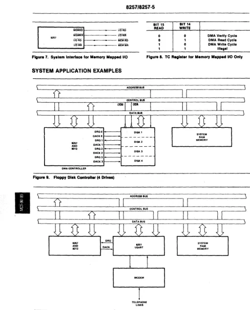
GENERAL THEORY of OPERATION
The internal operation of a floppy disk operating system is
probably the most complicated part of a micro-computer system. The
hardware and software interact very closely, and therefore a very
strong knowledge of 8080 assembly language and common logic operations
is desirable to understand this section. Knowledge of the IEEE S-100
standard is also desirable, as there are some changes that have been
made to the S-100 bus with this new specification. The IEEE S-100
Standard has been enclosed with this manual in the appendix, along
with the data sheets for the rest of the integrated circuits used on
the interface.
The heart of the Double Density interface is the 1791/1793 Floppy
Disk Controller Chip. This chip is very similar to the 1771 in
operation, but now includes all the functions necessary to run Double
Density. For your convenience, the 1791/1793 data sheet is included
in the appendix.
The interface may be broken down into subsections as follows:
1. 1791/1793 disk controller chip.
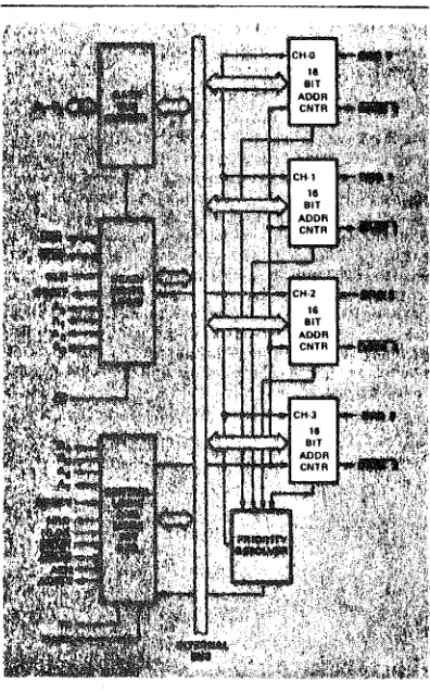
2. 8257 Direct Memory Access Controller chip. 3. Phase Locked Loop circuit.
4. Write Precompensation circuit.
5. General Drive and Computer interface.
The 1791/1793 controls the actual reading or writing to the floppy
disk, and in which density this will happen. The floppy controller
chip contains 4 internal registers which are programmed by the
computer through it's data and address lines. the four registers are
as follows:
1. status register 2. track register 3. sector register
4. data register
Review of the data sheet will help in understanding each function of
these 4 registers.
DDEN is used to control in which density the floppy disk controller
chip will be operating. Low equals Double Density, High equals Single Density.
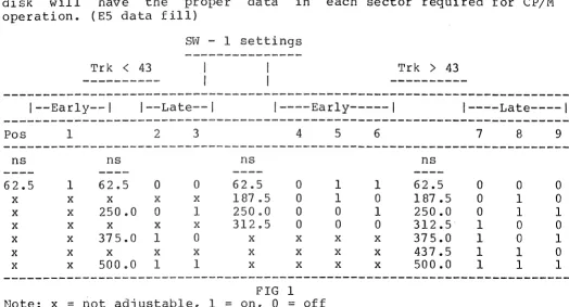
EARLY and LATE control the Write Precompensation of the data being
written to the disk. These two signals along with the TRK
>
43 linecontrol the amount of shift in time the bit that is being written to
the disk is subjected. Precompensation during writing is a must
because of the bit packing on the meaiurn of the disk.
This interface also has provisions for precompensation on tracks
<
43, and it is recommended that a small amount be used. The amount of
precompensation is a switch selection, and will be explained in the
jumper options.
READ GATE is an output used for synchronization of the data
seperator circuit during read operations. A high on this pin inaicates
GENERAL THEORY of OPERATION
that a field of 'ones' (or zeros) has been found in the inner record
gaps of the disk.
The 8257 Direct Memory Access Controller chip controls the actual
transfer of computer data between the disk and computer. This device
can be thought of as a high speed semi-intelligent cpu in its
operation. It contains 16 registers of which only 3 are used by this
floppy disk interface board. One is a command register, and the other
two are byte pair data registers. During read and write operations,
the 8257 must be initialized with the byte transfer count, the address of where the data is to go, and the type of transfer that is to occur,
such as read or write. The 8257 can transfer up to 16384 bytes of
data, and put it into any memory locations within a normal 8080's
addressing range •. The important aspect about the 8257 is that it will
transfer data to or from memory without the need of any cpu
intervention other than being initally programmed by the cpu. After i t
has been programmed, i t alone transfers the data, and in fact removes
the cpu from the S-100 bus during these transfers. In-depth
information about the 8257 is available in the INTEL data catalog ana
in the appendix of this manual.
The Phase Locked Loop circuitry on this interface is necessary for reliable data recovery, especially while running under double density.
It1s function is to remove effects of data fluctuations during READ
operations which may be the result of drive speed or power line
changes, and general system noise. The Phase Locked Loop is used
during Single and Double Density operation. This is accomplished by
logic on the interface and is controlled by the DDEN line and an
internal hardware latch. Tri-state switching is used to select the
master oscillator timing clock. When in Single Density, the master
clock is equal to 8 Mhz. Double Density selection causes the master
clock to change to 16 Mhz. A close examination of the schematic will
show these logic changes during density selects.
The write precompensation is in general terms really a count down
circuit, controlled by the EARLY, LATE, and TRK
>
43 lines duringwriting operations. This applies only when operating in double
density, as the EARLY and LATE signals are not active during single
density. The count down circuit is clocked by the 16 Mhz master
oscillator circuit. The amount of precompensation is determined by
the preset value jammed into the 74LS161 from the EARLY or LATE pins
of the floppy chip. After this value is loaded, the 74LS161 counts
until it reaches zero, at which time i t writes the data to the disk.
The effect of this is to delay the time the bit would have been
written to the disk, until it is actually written. The smallest amount of precompensation that may be realized from this circuit is:
1 / 16 Mhz = 62.5nsec.
Jumpers provided on the interface have been selected for optimum drive
performance. Selection is based on manufacturer's recommendations for
the drive in use, and our testing here at Tarbell Electronics.
The computer interface for this board is based on the IEEE S-100
bus interface specification. It is not radically different from the
old S-100 bus design, and should run with most S-100 products on the
GENERAL THEORY of OPERATION
market. If you have any questions about your interface cards, check
the section on S-100 compatible products in our manual.
The Disk Interface occupies an address range from EO-EF hex for the
DMA controller portion and FB-FD hex for the disk controller portion.
A jumper is provided to allow the address range to be moved to 60-6F
hex and 78-7D hex respectively, to avoid address conflicts with
exsiting computer boards you may have in your system. This is
explained in the jumper options section. The address ports are used
as follows:
EO hex El hex EB hex F8 hex FB hex F9 hex FA hex FB hex FC hex FC hex FD hex FD hex
8257 address register (must be two bytes to this port) 8257 word count register (must be two bytes to this port) 8257 command register (1 byte)
disk command port (input) disk status port (output) disk track port (input/output) disk sector port (input/output) disk data port (input/output) wait control port (input) drive select port (output)
DMA end of operation port (input) extended address port (output)
The extended address port (FD hex), allows the DMA controller to
transfer data to and from memory beyond the normal 64k range of the
8080 cpu. This function is avalible for both read and write operations
using the disk interface. The extended address lines are provided on
the S-100 bus as described in the IEEE S-100 bus interface
specification. The extended lines are Al6-A23.
To use the extended address function, user written software must
supply an 8 bit value corresponding to the bank at memory you want to
access, out to port FD hex before any read or write operations occur
with the disk interface. During DMA operation, this 8 bit latch is
enabled, placing its contents onto the extended address lines. The
output of this latch is normally tri-state until the DMA controller
becomes active. Also, this latch may be programmed at any time with
any value you wish, except during an actual transfer by the DMA
controller. You could even change this latch value between byte
transfers if you wish. With optional decoding on memory boards,
possible memory capacities can be theoretically 8 banks of 64k
(512kbytes), to 256 banks of 64k (16 Megabytes).
The interface is set up for Shugart 8" compatible drives, which
means drives with a Shugart interface such as Shugart 800/801 and
Siemens FDD 100-8,120-8, and 220-8 will interface directly to the
controller board. There are many drives which fall into this catagory
and we will be supplying updates as we go along for your convenience.
At this time we at Tarbell Electronics have run the Shugart 800/801
and all 8" drives made by Siemens. This includes both single and
double density. Persci drives model 270/277's are now supported with
this interface. See the section on jumpers for an explanation and
changes which must be made to support Persci drives.
DETAIL THEORY of OPERATION
This section of the manual will deal in depth with the theory of
operation of the double density board. The explanation will be broken
down into sections within the board design.
The following logic notation will be used: XX'= The logic name XX not, or the inversion of XX.
1. RESET circuit
The floppy disk interface receives it's reset from line 75
(PRESET) on the S-100 bus whenever a power on sequence is initiated or
whenever a RESET on the front panel of the computer is pushed. This
line is active low (0) whenever a reset is pushed. The result of
pushing a reset is to cause the floppy disk controller chip to do a
restore of drive Oto the home position, reset the DMA controller chip
to the idle state, and the latch (046), which is used for drive
select, density select, and side select, to be cleared to the
following condition, (a.) select drive O, (b.) select single density, and (c.} select side O.
The reset line from the bus is first inverted by 09 (7404) to
provide an active high (1) signal for the DMA controller chip 029
(8257). This signal is inverted again to provide an active low (O)
reset for floppy controller chip, 031 (1791/1793}, and for 046
(74LS174) an 6 bit latch. This active low reset signal also turns on
the bootstrap circuit by pulling the preset line of 035 low.
2. BOOTSTRAP Circuit
The bootstrap circuit is enabled during a power up sequence or
from the front panel reset switch. The reset causes a preset of
flip-flop 035, a 7474 D-toggle flip flop, causing i t ' s output, pin 5, to go high (1). This output is tied to one of three (3) inputs of 033,
a 7411 3-input AND gate. The two other inputs come from the S-100 bus
interface pins 47 (SMEMR), and 78 (PDBIN). The output of 033 is tied
to the input of a 7406 (087), which drives the PHANTOM line (67) low.
033 also also drives a hex inverter 034, which drives the chip select
line on the Bootstrap Prom low, enabling the data outputs of the prom
on to the data bus. When run is enabled on the computer, the contents
of the prom are read onto the data bus and into the cpu as
instructions. Because this prom is only 32 bytes long, the method of
disabling it when it has completed all its instructions, is to look at
address line 5 of the S-100 bus. This address line is fed to one of
the inputs of 047, a 7421 4-input AND gate. The other three (3) lines
in to 047 are PHASE l (25) ,PSYNC (76), and SMI (44). When the
computer has read all 32 bytes of the prom, and an attempt to read the
33rd byte is tried, address line 5 will go high (1), which causes one
input of 047 to go high. The three other inputs of 047 will also go
high, causing its output to go high. This output line then causes the
output of 026, a 7404 inverter, to go LOW (0), resetting 035. When
this flip flop is reset, its output, pin 5, will go low, disabling
DETAIL THEORY of OPERATION
both the PHANTOM line and the Bootstrap Prom chip select* This action
releases the the bus data lines back the their normal operating
condition. During power up of your system, if you wish to disable the
bootstrap circuitry, and have a front panel, you may raise
address-data switch 5 and hit examinee This will turn off the
bootstrap circuit, allowing you to access all computer memory. The
bootstrap may be defeated entirely by using jumpers E8 to E9 on the
disk interface. Using jumpers E9 to ElO enables the bootstrap during
each reset. Below is a listing of the bootstrap prom for both the
standard Tarbell disk ports, and for our non-standard disl~ ports. Our
standard prom is model# 100 and our non-standard prom is model# 101.
Model 101 is for people who wish to run the disk interface at
addresses 60 to 7D hex.
STANDARD PROM BOOTSTRAP LISTING
0000
OOF8 = OOF8 =
OOF8 =
OOFA = OOFB = OOFC =
007D =
0000 DBFC 0002 AF 0003 6F 0004 67 0005 3C 0006 D3FA 0008 3E8C OOOA D3F8 OOOC DBFC OOOE B7 OOOF F21900 0012 DBFB 0014 77 0015 23 0016 C30COO 0019 DBF8 001B B7 OOlC CA7DOO OOlF 76
; DISK DCOM DSTAT SECT DDATA WAIT SBOOT ; BOOT: RLOOP: RDONE: ORG EQU EQU EQU EQU EQU EQU EQU IN XRA MOV MOV INR OUT MVI OUT IN ORA JP IN MOV INX JMP IN ORA JZ HLT
0 ;PROM RUNS AT LOC ZERO.
OF8H ;BASE ADDRESS OF DISK PORTS.
DISK ;COMMAND PORT.
DISK ;DISK STATUS PORT.
DISK+2 ;SECTOR PORT.
DISK+3 ;DATA PORT.
DISK+4 ;WAIT PORT.
007DH ;START OF SBOOT.
WAIT ;WAIT FOR HOME.(caused by reset)
A ;CLEAR ACCUM.
L,A ;CLEAR REG L.
H,A ;CLEAR REG H.
A ;SET A= 1.
SECT ;START AT SECTOR 1.
A,8CH ;READ THE SECTOR.
DCOM ; ISSUE THE COMMAND.
WAIT ;WAIT FOR DRQ OR INTRQ.
A ; SET FLAGS.
RDONE ;DONE IF INTRQ.
DDATA ;ELSE,GET A BYTE FROM DISK.
M,A ;PUT IT INTO MEMORY.
H ;BUMP POINTER.
RLOOP ;LOOP TILL DONE.
DSTAT ;READ DISK STATUS.
A ;SET THE FLAGS.
SBOOT ;IF ZERO, GOTO SBOOT.
;ELSE, DISK ERROR
DETAIL THEORY of OPERATION
NON-STANDARD BOOTSTRAP PROM LISTING
---~---~
0000 ORG 0 ;PROM RUNS AT LOC ZERO.
;
007 8 = DISK EQU 07 8H ;BASE ADDRESS OF DISK PORTS.
007 8
=
DCOM EQU DISK ;COMMAND PORT.007 8 = DSTAT EQU DISK ;DISK STATUS PORT.
007A = SECT EQU DISK+2 ;SECTOR PORT.
007B = DDATA EQU DISK+3 ;DATA PORT.
007C
=
WAIT EQU DISK+4 ;WAIT PORT.007D = SBOOT EQU 007DH ;START OF SBOOT.
.
8
0000 DB7C BOOT: IN WAIT ;WAIT FOR HOME.(caused by reset)
0002 AF XRA A ;CLEAR ACCUM.
0003 6F MOV L,A ;CLEAR REG L.
0004 67 MOV H,A ;CLEAR REG H.
0005 3C INR A ;SET A= 1.
0006 D37A OUT SECT ;START AT SECTOR 1.
0008 3E8C MVI A,8CH ;READ THE SECTOR.
OOOA D378 OUT DCOM ;ISSUE THE COMMAND.
OOOC DB7C RLOOP: IN WAIT ;WAIT FOR DRQ OR INTRQ.
OOOE B7 ORA A ; SET FLAGS.
OOOF F21900 JP RDONE ;DONE IF INTRQ.
0012 DB7B IN DDATA ;ELSE,GET A BYTE FROM DISK.
0014 77 MOV M,A ;PUT IT INTO MEMORY.
0015 23 INX H ;BUMP POINTER.
0016 C30COO JMP RLOOP ;LOOP TILL DONE.
0019 DB78 RDONE: IN DSTAT ;READ DISK STATUS.
001B B7 ORA A ;SET THE FLAGS.
OOlC CA7DOO JZ SBOOT ;IF ZERO, GOTO SBOOT.
OOlF 76 HLT ;ELSE, DISK ERROR
3. ADDRESS SELECTION
The double density controller board is selected based on the low order 8 address line values presented to the interface during an input or output instruction. The normal address range for this board is from
EO hex to FD hex. There are provisions for changing the address range
from 60 hex to 7D hex by means of jumpers E4,E5,and E6.
The base address for the DMA controller (8257) is EO hex, with
all possible 16 address from EO to EF hex available for use by the DMA
controller chip. 033, a three input AND gate, is used to determine
the base address of EO hex by tying address lines A7,A6,and AS to its
three inputs. You will notice that an inverter, U34, is in between one
input of U33, and address line A7. By selecting the proper jumper at
E4,E5, and E6, you may select a base address of either EO hex or 60
hex. By using the inverter, 034, you will select the base address of
60 hex. By not using the 034, but using the jumper which bypasses U34,
DETAIL
THEORY of OPERATION
AND'ed
with the inversion of A4 through U26. This gate (U48) is used
to allow selections from EO hex to EF hex for I/0 operations with
the
DMA
controller. The output of U48 drives one of the inputs to U43 for
selecting the DMA controller chip select line. The other input for U43
(7400), comes from U45 (7432). U45 determines whether the current
I/0
operation
is an
Input
or
an
Output with the interface board. The
. signals SINP and SOUT are two status lines from the CPU card used to
determine
the I/0 operation. Because these two signals will not occur
together, they may be OR'ed together through U43 to provide
just one
general signal for I/0 operation decoding.
Disk I/0 ports for the 1791/1793
floppy
controller chip are
decoded by U47, a 4 input AND gate. One input to U47 comes from U33's
output, which is the address decode for the base address of Ex hex
or
6x
hex.
Address lines 4 and 3 are tied to two of the other inputs of
U47. Address line 2 is inverted through U26 (7404) and is the
fourth
input
to U47.
The
Output of
U47
goes
high whenever any of the
following address appear on the address bus,F8,F9,FA,and FB hex.
Ports FC and FD hex are decoded by U27 (74LS138). The output
of
gate U33 is used for the enable input of U27. The other two enables of
U27 are an enable when low function and are derived from the inversion
of
address lines 3
and
4
through two inverters U26. The output of
inverter U26 pin 10 also goes to one input of gate U48.
If address
line 4
is high
(eg. Port FC), The output of U26 pin 10 will be low
(O) ,causing the output of gate U48 to be low, disabling the selection
of
any port with the base address of Ex hex. The 3 low address lines,
AO,Al, and A2 determine which port is selected on the output of
U27.
Also,
even though the low 3 lines of the address bus are used by U27,
only two of the possible 8 ports are used by the disk interface board.
Port decodes from U27 for F8,F9,FA, and FB are not used. Only Ports FC
and FD hex are used.
4. DISK CONTROL circuit
The 1791/1793 Floppy disk formatter/controller chip performs all
the functions necessary to read or write data to a floppy disk
drive.
Both single and double density storage capabilities are supported. The
chip is compatible with the IBM 3740 (FM) data format,IBM System 34
(MFM), or may
be
operated non-standard by
using
the controllers
variable length sector capability.
The floppy controller chip contains five
(5)internal
registers
that can
be read or be written to. These registers are used to write
commands, read status, and read and write data to and from the
floppy
disk drive. These five registers are selected by providing the proper
binary code on the AO and Al lines of the floppy chip in conjunction
with either
a
read or write operation.
The
registers and their
addresses are as follows:
DETAIL THEORY of OPERATION
CS' Al AO RE'= 0 WE'=O
---0 0 0 0
1
0 0
1
1X 0
1
0
1
X
Status Reg Track Reg Sector Reg Data Reg Deselected
Command Reg Track Reg Sector Reg Data Reg Deselected
The five internal registers of the floppy controller chip are
accessed through the internal interface data bus. The internal data
bus is buffered by U71 (8208) and U72 (8208). U71 and U72 are 8 bit
bi-directional transcievers which are used as bi-directional data
buffers between the computer S-100 bus and the floppy disk interface
internal data bus. These transceivers allow data travel in either
direction depending upon whether the TRANS/REC' pin (11) is high or
low. To program the floppy controller chip, AO,Al are selected for
the desired operation. Write enable of U31 is made active low by
processor signal SOUT and PWR' gated together by U23 (7400). The data
that the CPU wishes to program the floppy controller with, is now
placed on the DOO - D07 lines of the CPU card. This data is then
presented to U71. Because we are not in the DMA mode of operation, the TRANS/REC' pin is already pulled low, causing the transceiver to be in
the receive mode. The data is then passed through U71 onto the
internal data bus and into the floppy chip DALO DAL? lines. Chip
select, pin 3, of U31 is made active low by U48 (7408) output. One
input of U48 comes from the OMA controller and the other input is from
U43 which is the gating of the address port and the I/0 mode desired.
In this case, since we are programming the floppy controller, any port
address in the range of F8 - FB hex gated together with SOUT will
cause the data to be written to the controller chip.
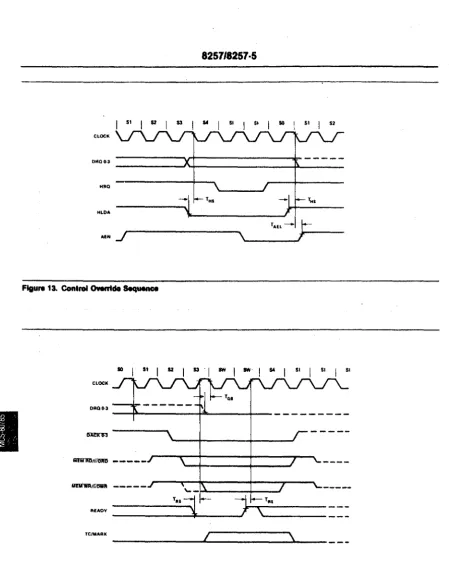
5. Direct Memory Access
The sequence of operations for a OMA access is as follows:
A. The Basic Input Output System (BIOS part of CP/M) program sends
a series of initialization bytes to the 8257. These include
the starting address in memory for the data, the number of
bytes to transfer, and the type of command (read, write, verify)
which is being requested. The port numbers for these and other
transfers are listed on page 3-3 in this manual.
B. The BIOS then sends track number, sector number, and type of
command (read or write) to the 1793.
c.
The 1793 then causes the head to load against the media (weare assuming we're already on the correct track). When the
1793 finds a sector header that matches the track and sector number in i t ' s registers, and is ready to write or read the first byte, it activates its DRQ line, which is fed to the
8257. This signifies that it is ready to transfer a byte.
D. Soon after receiving the input on its DRQO line, the 8257
makes its HRQ line go high. This is fed through an OR gate
DETAIL THEORY of OPERATION
to S-100 bus line PHOLD'. This notifies the CPU that there is a DMA request pending.
E. When the CPU finishes the cycle it is currently in, it sends back a PHLDA signal over the S-100 bus to the HLDA input on the 8257. This tells the 8257 that its DMA request has been granted, and that the CPU is in a HOLD state.
F. The 8257 then activates its AEN line, which indicates that it has a valid address on AO to A7 and DO to D7. This signal is ORed with the HRQ to keep PHOLD' active, and disables the CPU address and data lines using S-100 bus lines DO DSB' and
ADR DSB'. AEN also is fed to (U41) and (U67), which gates the DD board's own status and control lines onto the S-100 bus
(PWR', PDBIN, SMEMR, SINP, SOUT, PSYNC, MWRITE, SINTA, SHLTA, SMl). G. A short time later, the 8257 activates its DACKO' line, which
disables the CPU's status and control lines, using S-100 bus lines STAT DSB' and C/C DSB'. The time between step F and G provides the overlap time, during which both our DD.board
and the CPU board have control of these status and control lines. H. At the same time as the DACKO' line is activated, the 8257
activates either its MEMR' line, or