Abstract—Convolutional neural network (CNN) is a machine learning algorithm that plays an important role in image recognition and classification applications. In order to enable the IoT endpoint SoC with limited computing capability to support CNN algorithm, a multifunctional CNN accelerator is proposed which implements major computing components in CNN by hardware. Each computing module is arbitrarily combined by parameter configuration to complete the complex network calculation. In this paper, a SoC with Cortex-M3 kernel is implemented in FPGA as a test platform to verify the performance of the designed accelerator. Evaluation of design scheme is performed by comparing the execute time of the Lenet-5 network on the designed SoC, Intel 7500, Samsung S5P6818 and Allwinner H3.The comparison results show that the compact accelerator proposed in this paper makes the CNN computing power of the SoC based on the Cortex-M3 kernel exceeds the Cortex-A53 kernel, and its CNN computing power per unit frequency reaches 6 times that of the Intel 7500.
Index Terms— CNN accelerator, IoT endpoint SoC, Multifunctional, Lenet-5
I. INTRODUCTION
ost recently, with the evolution of internet of things (IoT) technology and rapid development of artificial intelligence (AI), smart IoT with the advantage of AI and IoT technology has gradually become a research hotspot. Combining big data with the complex algorithm, smart IoT technology brings profound changes to the IoT as well as puts forward new challenges to the organization structure of the IoT systems [1]. Although the edge computing theory can guide us to solve this severe problem, unfortunately, a great deal of IoT endpoint SoC have limited computing power in order to pursue compact structure and low power consumption. That is not enough to meet the computing capabilities and requirements of the AI algorithm such as CNN [2]. Not only that, researchers who dedicated to the AI computation acceleration have not paid enough attention to AI acceleration in IoT devices. It is of great practical
Manuscript received July 2, 2018. This work was supported in part by the National Natural Science Foundation of China (No. 61774086, No. 61376025), the Natural Science Foundation of Jiangsu Province (BK20160806), and the Fundamental Research Funds for Central Universities (No. NS2017023).
Y. Zhang is with College of Electronic and Information Engineering, Nanjing University of Aeronautics and Astronautics, Nanjing, 211100, China (e-mail: [email protected]).
N. Wu is with the College of Electronic and Information Engineering, Nanjing University of Aeronautics and Astronautics, Nanjing, 211100, China (e-mail: [email protected]).
F. Zhou and Muhammad Rehan Yahya are with the College of Electronic and Information Engineering, Nanjing University of Aeronautics and Astronautics, Nanjing, 211100, China.
significance to design a compact CNN accelerator suitable for SoC of the IoT endpoint.
CNN is an alternative type of neural network that can be used to reduce spectral variations and model spectral correlations which exist in signals [3]. Nowadays, the research on CNN acceleration based on ASIC/FPGA can be divided into two categories, including unfold the network structure through hardware or only accelerate the convolution operation. In reference [4-6], the vast majority of the structure in networks is expanded and implemented by hardware to speed up the computation of CNN networks. This measure can always get maximum acceleration performance but with reduced flexibility and resource consumption. Hence, it is not applicable to the IoT where the resource is tightly constrained. In reference [7], a convolution cell is added to the CPU kernel, enabling the processor to accelerate the calculation of CNN through convolution instructions. Although this method makes the circuit compact but its speed-up ratio is fairly low.
Based on the comprehensive consideration of the circuit area and acceleration performance, a compact CNN accelerator is proposed and designed in this paper. Our design includes a convolution data loading module with low bandwidth occupation, a high throughput storage unit and four multifunction convolution network accelerating chains. The rest of the article is organized as follows:
1) The framework and crucial parts of the CNN accelerator are introduced in section II that includes the design of storage channel, a matrix convolution unit with low bandwidth occupation and the implementation of multifunction convolution network accelerating chain.
2) Based on the Cortex-M3 kernel, a SoC with CNN accelerator is designed as the verification platform. Beyond that, the Lenet-5 network is transplanted on the designed platform to evaluate the acceleration performance of the accelerator.
3) After completing the verification platform construction and Lenet-5 transplantation, we have demonstrated the acceleration performance and resource consumption of the CNN accelerator in section IV.
4) Finally, section V concludes this paper and proposed future work is discussed at the end of this article.
II.CNNACCELERATOR DESIGN
A.Accelerator structure
CNN is a class of deep and feed-forward artificial neural networks, most commonly applied to analyzing visual imagery. The primary arithmetic element of CNN includes 2D-matrix convolution, nonlinear activation and pooling operation. According to statistics, convolution operation
Design of Multifunctional Convolutional Neural
Network Accelerator for IoT Endpoint SoC
Yuanyuan Zhang, Ning Wu, Fang Zhou and Muhammad Rehan Yahya
takes about 90% of the total network computing time [8]. Based on the characteristics of CNN and combined with the requirements of the compact structure and low power consumption of IoT system, we design an efficient CNN accelerator for IoT system. The overall structure of the designed unit is shown in the Fig. 1.
The accelerating module contains the source matrix data loading module, a convolution kernel cache, two ping-pong buffer blocks and four accelerated computing chains. By using these modules, the designed accelerating module can complete convolution, activation and subsampling operation with four convolution kernels simultaneously.
B.Design of storage channel
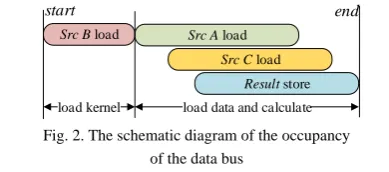
CNN computing requires a large amount of data access and design of the storage channel for the unit directly affect the acceleration performance. The accelerator in this paper includes a source matrix read-channel (Src A), four convolution kernel matrix read-channels (Src B), four accumulative value read-channels (Src C) and four calculation results store-channels (Result). According to the calculation process of the CNN, the occupancy order of the data bus is shown in Fig. 2
It is apparent from Fig. 2 that there is a data bus competition relationship among Src A, Src C and Result. On top of this, data access of the four accelerating chains will occupy 128-bit memory bandwidth, which poses a great challenge to the design of memory.
To solve the bus competition among these three channels, two separate storage units are used which can map Src A, Src B and Src C to different storage areas through parameter configuration. Simultaneously, for storing the 128-bit width data generated by four accelerating chains in real time, a memory unit is designed in this paper that uses four dual-port RAM (DP-RAM) to form a dual port storage block that is
the calculation results or to read the Src C, while the other port is configured as Src A reading-channel or connecting with SoC bus according to the configuration.
C.Convolution data loading unit with low bandwidth occupation
As the critical part in CNN, 2D matrix convolutions account for more than 90% of the total computation. A large amount of data is required in the calculation of 2D matrix convolution that consumes tremendous bus bandwidth, thus affecting the data processing efficiency of the whole system. In this paper, a matrix data reading unit with low bandwidth occupation is designed to improve the throughput of the data, which takes advantage of high data repetition rate of 2D matrix convolution.
The loading unit of convolution matrix consists of a matrix data reading unit and a cyclic queue, where matrix data is read by column priority. We take a matrix with 5*5 size and a convolution kernel with 3*3 size as an example; its convolution data loading process is shown in the Fig. 4.
It can be seen from the Fig. 4 that the convolution of an image with a 5*5 size and a kernel of 3*3 needs to read 45 data from the source address, which is far less than the 81 data needed for actual computing and its advantage is more obvious when the width of source matrix is larger. Assuming that source matrix is N*N, the size of the convolution kernel is k*k and total amount of data to read by using this convolution data loading unit can be expressed as:
(k*k+ N-k *k * N-k+ =N*k* N-k+( ) ) ( 1) ( 1) (1) The actual amount of data needed for convolution is:
( 1) ( 1)
k*k* N-k+ * N-k+ (2) In conclusion, the bandwidth optimization rate when using this module to read data is:
( 1)
1
( 1) ( 1)
= - N*k* N-k+
k*k* N-k+ * N-k+ (3)
Src B load Src A load
Src C load
Result store
load kernel
start end
[image:2.595.310.504.95.184.2]load data and calculate
[image:2.595.70.266.129.303.2]Fig. 2. The schematic diagram of the occupancy of the data bus
Fig. 1. The architecture of the accelerator
dual port ram 1
dual port ram 2
dual port ram 3
dual port ram 4
sha
re
d
bu
s
SoC data bus MU
X
Src a read
chain1 result/
Src c
chain2 result/
Src c
chain3 result/
Src c
chain4 result/
Src c
[image:2.595.317.545.433.555.2]block ram
Fig. 3. The structure of the DP-RAM memory block
6 7 8 9 10
1 2 3 4 5
16 17 18 19 20
11 12 13 14 15
21 22 23 24 25 4 9 14 5 10 15 3 8 13
write start read start
4 9 14 2 7 12 3 8 13
write start read start
1 6 11 2 7 12 3 8 13
write start read start
1st unit:
2st unit:
3st unit:
[image:2.595.70.265.532.618.2]Taking the first level of Alexnet network as an example, where N is 224 and K is 11, so is equal to 90.485% [10]. Analogously, the optimization rate of the first layer in Lenet-5 is 64.46%.
D.Design of multi-function configurable acceleration module The core of the accelerating unit designed in this paper is four multi-function configurable accelerating chains. Each accelerating chain can be divided into four functional modules: convolution, floating-point addition, activation and subsampling. These chains can complete any combination of these four functions according to the configuration to realize the design of multi-function configurable accelerating module. The functions of these chains include matrix point product, matrix convolution, matrix addition, activation, matrix transposing and matrix subsampling. Some configuration parameters and example configurations of several different functions are shown in Table I.
III. VERIFICATION PLATFORM CONSTRUCTION
A.Design of verification platform based on Cortex-M3 A MCU kernel launched by ARM, Cortex-M3 (CM3) achieved a good balance between power and performance, its Dhrystone score is 1.25 DMIPS/MHz which is enough to meet the processing requirement of IoT node devices.
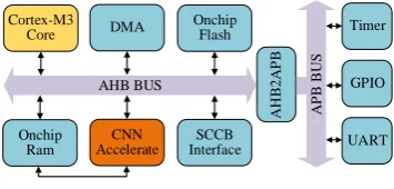
[image:3.595.340.518.71.156.2]In order to evaluate the performance of the designed unit, an IoT SoC with the CNN accelerating module based on the CM3 kernel is designed. The SoC structure is shown in the Fig. 5.
The SoC built includes necessary modules such as 128KB RAM, 128KB ROM and common peripherals such as GPIO and UART. AHB and APB are used as the interconnected bus for SoC, where, high-speed devices such as DMA and CNN accelerator are connected with the kernel through AHB bus and low-speed devices such as GPIO are bridged through the
APB bus.
B.Implementation of Lenet-5 network
The Lenet-5 which proposed in 1994 is considered to be one of the earliest and most classical convolution neural networks. With the deepening of CNN research, a series of more effective CNN structures have been put forward but as a classic structure, Lenet-5 is still widely used to evaluate the performance of CNN acceleration units.
The structure of Lenet-5 is shown in Fig. 6. Its structure can be divided into five hidden layers, which are the convolution layer with six convolution kernels, a subsampling layer S1, a partially connected layer containing sixteen convolution kernels, a subsampling layer S2 and a fully connected layer which contains ten convolution kernels. More information about the Lenet-5 structure can be referred in [9].
In Lenet-5, the calculation of the partially connected layer is the most complicated because results of this layer are related to the multiple or all output of the previous layer, so we mainly focus on the implementation of that layer. Accelerator designed in this paper has the function of convolving the source data with four kernels simultaneously and can also add the convolution result with another matrix. Based on this feature, we implemented partially connected layer as shown in Fig. 7.
The table on the left of Fig. 7 describes the relationship between the partially connected layer and the previous layer. TABLE I
PARAMETER CONFIGURATION TABLE FOR TWO FUNCTIONS
Name Range Description Lenet5
1st layer
8*8 dolt_mult
Mode 0~15
Bit0:conv work Bit1:float add Bit2:relu work Bit3:pooling work
15 1
Ch_num 1~4 Accelerating chain
number 4 4
Src_width 0~255 Src matrix width 32 8
Pool_width 1~8 Pooling unit width 2 --
Out_num 0~65535 Result number 784 64
Unit_width 0~32 Kernel width 5 8
Cortex-M3 Core
AHB BUS
Onchip Flash
Onchip Ram
CNN Accelerate
A
P
B BU
S
DMA
SCCB Interface
A
H
B
2
A
P
B
Timer
GPIO
UART
Fig. 5. SoC structure based on CM3
=
Pool( Relu( Src5*k0+e0 ) )
...
... Pool( Relu( Src5*k1+e1 ) )
Pool( Relu( Src5*k15+e15 ) )
...
=Src 0 * a0
a1
...
a15
k0 k1
...
k15
=Src 1 * b0
b1
...
b15
+ k0 k1
...
k15 a0 a1
...
[image:3.595.308.546.291.374.2]a15
Fig. 7. The calculation process of partial connecting layer
convolutions
subsampleconvolutionssubsampleexpansion full connection
Input image
32*32 28*28 14*14 10*10 5*5 400*1 10*1
[image:3.595.57.542.652.756.2]As shown in the graph, we extract the six matrices from the S1 layer in turn and convolution with the corresponding matrix kernels respectively according to the connection relationship of the Lenet-5 C2 layer. For 2th to 6th matrices of S1, in addition to convolution with the kernels it should also be added to the previous round of computation.
Through the analysis of the structure of the Lenet-5 network using the accelerator designed in this paper to complete the Lenet-5, the concrete realization process can be segmented into four steps as Table II.
IV. TEST RESULTS AND ANALYSIS
A.Performance analysis of acceleration unit
In this paper, we select a desktop processor and two high-performance application processors as performance evaluation objects. In order to estimate the execution time of Lenet-5 network on different hardware and software platforms, we use C language to realize forward propagation of Lenet-5. The forward propagation program of Lenet-5 is run on Intel 7500, Cortex A7 and Cortex A53 to compare with SoC designed in this paper respectively. The execute time of each platform is shown in Table 3. The program written in this article only uses the single thread so for multi-core processors only one core is used.
According to the results, we can see that the use of the accelerator designed makes a compact IoT SoC with the 50MHz obtain more powerful CNN calculation capability than the Cortex A53 kernel. Its CNN computing power under unit frequency is 6 times that of Intel 7500.
B.Analysis of resource consumption
To design a CNN accelerator suitable for IoT systems compact structure is a key principle during design process. In order to complete the evaluation of resource consumption of the accelerating module, we have implemented our designed circuit on FPGA. The model of FPGA is Xilinx Zynq7020, and the synthesize tool is Vivado 17.2. The resource
consumption comparison between the designed module in this paper and the reference [6, 4] is shown in Table IV.
Compared with the other two designs, the accelerating unit of our proposed structure does not pursue high acceleration performance but rather it obtains most suitable acceleration ratio with small resource consumption and conforms to design concept of IoT devices.
V.CONCLUSION
In this paper, we have proposed and implemented a compact CNN accelerator to improve the CNN computing power of endpoint devices in IoT applications. The experimental results reveal that the proposed acceleration module can make SoC of Cortex-M3 kernel get more neural network computation ability than Cortex A53 at the cost of small resource consumption. However, our design still uses floating-point data in the process of CNN computing. In fact, according to the current research, the use of fixed-point type data can further reduce the consumption of resources with little loss of recognition accuracy [11]. In future, we seek to further develop and achieve this goal.
REFERENCES
[1] Sheth A, “Internet of Things to Smart IoT Through Semantic, Cognitive, and Perceptual Computing,” IEEE Educational Activities
Department, 2016.
[2] Calo S B, Touna M, Verma D C, et al, “Edge computing architecture for applying AI to IoT,” IEEE International Conference on Big Data, 2018, pp. 3012-3016.
[3] Sainath T N, Kingsbury B, Saon G, et al, “Deep Convolutional Neural Networks for large-scale speech tasks,” Neural Networks, 2015, vol. 64, pp. 39-48.
[4] Zhang C, Li P, Sun G, et al, “Optimizing FPGA-based Accelerator Design for Deep Convolutional Neural Networks,” Acm/sigda
International Symposium on Field-Programmable Gate Arrays, 2015,
pp. 161-170.
[5] Zhou Y, Jiang J, “An FPGA-based accelerator implementation for deep convolutional neural networks,” International Conference on
Computer Science and Network Technology, 2016, pp. 829-832.
[6] Guo K, Sui L, Qiu J, et al, “Angel-Eye: A Complete Design Flow for Mapping CNN onto Embedded FPGA,” IEEE Transactions on
Computer-Aided Design of Integrated Circuits and Systems, 2017, vol.
99, pp. 1-1.
[7] Conti F, Schilling R, Schiavone P D, et al, “An IoT Endpoint System-on-Chip for Secure and Energy-Efficient Near-Sensor Analytics,” IEEE Transactions on Circuits & Systems I Regular
Papers, 2016, vol. 99, pp. 1-14.
[8] Jing, Chang, and S. Jin, “An efficient implementation of 2D convolution in CNN,” Ieice Electronics Express, 2016, vol. 14, no. 22, pp.20161134-20161134.
[9] Haykin S, Kosko B, “GradientBased Learning Applied to Document Recognition,” Wiley-IEEE Press, 2009, pp. 306-351.
[10] Krizhevsky A, Sutskever I, Hinton G E. “ImageNet classification with deep convolutional neural networks,” International Conference on
Neural Information Processing Systems. , 2012, vol. 60, pp.
1097-1105.
[11] Anwar S, Hwang K, Sung W, “Fixed point optimization of deep convolutional neural networks for object recognition,” IEEE
International Conference on Acoustics, Speech and Signal Processing,
2015, pp. 1131-1135. TABLE II
THE COMPUTING PROCESS OF LENET-5 USING THE ACCELERATION UNIT
Layer Calculation Methods Description
C1 & S1 0 5 0 5
1 1 1 1
[S~S] pool r el u S[ [ * [K~K] ] ]
Convolution and subsampling
C2 & S2
0 15 0 0 15
2 2 1 2 2
[S~S ] S * [K~K ]
0 15 1 0 15 0 15
2 2 1 2 2 2 2
[S~S ] S * [K~K ][S~S ] ....
0 15 15 0 15
2 2 1 2 2
0 15
2 2
[ ~ ] [ [ * [ ~ ] [ ~ ] ]
S S pool r el u S K K
S S
Partially connection and subsampling
S3 0 15
3 [ 2~ 2]
S S S Expansion
S4 0 9 0 9
4 4 3 3 3
[S~S] S * [K~K] Full connection
TABLE III
COMPARISON OF LENET EXECUTE TIME UNDER DIFFERENT PLATFORMS
SoC Core
Frequency
Latency/ Image
Acceleration ratio of unit frequency
Intel i5 7500 3.5GHz 1ms 6.36
Samsung
S5P6818 1.4GHz 12.3ms 31.3
AllWinner
H3 1.6GHz 15.3ms 44.5
Ours 50MHz 11ms --
TABLE IV
RESOURCE CONSUMPTION ASSESSMENT OF ACCELERATION UNIT
LUT FF BRAM DSP
Ours 5717 6207 39 20
[6] 29867 35489 85.5 190