TABLE OF CONTENTS
INTRODUCTION
PHYSICAL DESCRIPTION. Fixed Logic .
User Interface Logic
UNIBUS INTERFACE
USER LOGIC INTERFACE
THEORY OF OPERATION Data Bus.
Address Selection Logic Interrupt Logic
User Interface Logic
JUMPER CONNECTIONS Address Logic . Interrupt Logic
USER LOGIC EXPANSION MODULE
LOGIC DIAGRAM, MDB-1710 . . .
f:1[)B
MOB SYSTEMS, INC.1995 N. Batavia St. Orange, California 92665 714-998-6900
TWX: 910-593-1339
©Copyright 1977. MDB Systems, Inc. All rights reserved. DEC, PDP-II, Unibus are trademarks of Digital Equipment Corporation.
Page
1 2 2 2
2
4
5
6 6 7 8
9 9 9
10
MDB-1710
GENERAL-PURPOSE INTERFACE MODULE
INTRODUCTION
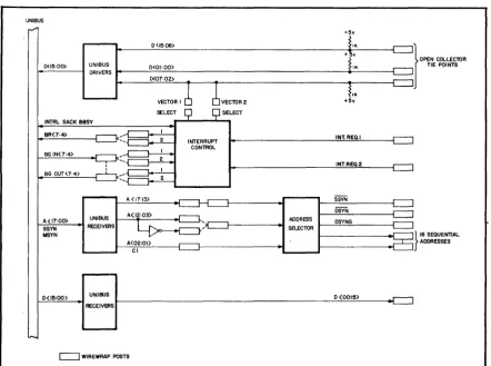
The MDB-I 71 0 General-Purpose Interface Module acts as an interface to transfer information between a Digital Equipment Corp. PDP-II Unibus™ and the user's peripheral device.
The MD1;l-1710 consists of a single quad module containing the following:
• fixed logic to interface with the PDP-II and with user's interface logic built on the module. Fixed logic includes receivers and drivers, device address selection and decoder logic, and dual interrupt vector logic (see figure 1).
• circuit board facilities and wire-wrap posts to accommodate up to 40 integrated-circuit devices. These facilities are used to build logic interfacing the fixed logic on the module with the user's peripheral device.
The MDB-1710 fits into either the DEC BB-Il, DD-IIA, or DD-IIB Peripheral Mounting Panel.
UNIBUS
0<15:00) UNIBUS
+fK
}
D(OI:OO) , _ _ _ _ _ _ _ _
---1+f~~K---~ O':E~lO"
1---1 DRIVERS
~---=c...:..:..:....=:...---INTRL SACK BBSY
BG OUTU:4>
A(17:00> SSYN MSYN
0(15:00)
UNIBUS RECEIVERS
UNIBUS RECEIVERS
~--~D~<0~7;~02~>~~-~---~~~--~c=J
A < 17:13>
A(02:01> CI
VECTOR I SELECT
INTERRUPT CONTROL
VECTOR 2 SELECT
~IK
+5v
~ ___ ---~I~NT.~.R~EQ~.I---~c=J
~ ___ - - - -__ -~I=NT=.R=~=.2~--~
~~ ADDRESS DSYNG
-~---~sruc~r-~~----~
_ _ _ _ _ _ _ _ _ _ _ _ _ D~<~00~:15_> _ _ _ _ _ .c=J
c:=J WIREWRAP POSTS
Figure 1 MDB-1710, Block Diagram
}
[image:3.614.94.537.355.684.2]PHYSICAL DESCRIPTION
FIXED LOGIC
Logic provided on the module consists of integrated-circuit devices in dual-in-line (DIP) packages; and wire-wrap posts used to select interrupt levels and vector addresses, to program the device address, and to make Unibus driver inputs and receiver outputs, and interface address and control lines, available for connection to user interface logic.
Fixed logic is connected to the Unibus through etched fingers that engage the printed-circuit board connector. The 1110dule may include three (optional) ribbon cable connectors for interconnection between the MDB-171 0 and the user's peripheral device or other MDB modules.
USER INTERFACE LOGIC
The module accommodates up to 40 integrated circuit devices in wire-wrap terminations. Sixteen positions (in locations 2H through 8H, and 2D through 8D) are dedicated for 14-pin DIP devices and have prewired power and ground connections (pins 14 and 7, respectively).
The remaining positions will also accommodate 14-pin devices, or 16-pin devices if jumpers connecting pins 7 and 8 are removed.
Columns I and 10 will accept devices with 22, 24, or 40 pins, as well as 14- or 16-pin devices. Use of three 24-pin devices, or two 40-pin devices, will reduce the number of possible 16-pin positions by four.
Columns 1 and 10 will also accept discrete components when space is not used for I-C devices. Wire-wrap posts are provided to accommodate discrete components in plated-through holes at 0.3-, 0.4-, and 0.6-inch centers.
All Unibus driver inputs and receiver outputs appear at wire-wrap posts for use in multiple-controller interfaces. Unibus driver inputs have pull-up resistors that permit using open-collector gates (7403 or equivalent) to OR-tie additional inputs to the drivers. Receiver outputs will handle up to 30 unit loads.
UNIBUS INTERFACE
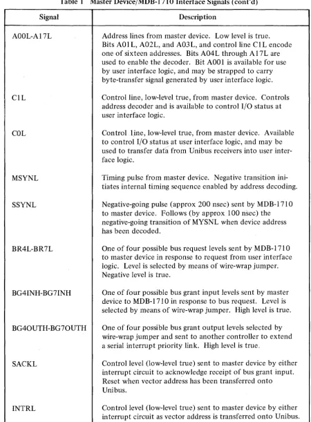
Table I lists signals at the Unibus/MDB-171 0 interface, and other signals that pass between the master device and the module.
Signal
DOOL-DI5L
INITL
Table I Master Device/MDB-171 0 Interface Signals Description
Unibus bidirectional data lines. Low (ground) is true, +3V is false.
Table 1 Master Device/MDB-1710 Interface Signals (cont'd)
Signal
AOOL-AI7L
CIL
COL
MSYNL
SSYNL
BR4L-BR7L
BG4 INH-BG 7INH
BG40UTH-BG 70UTH
SACKL
INTRL
BBSYL
Description
Address lines from master device. Low level is true. Bits AOIL, A02L, and A03L, and control line CIL encode one of sixteen addresses. Bits A04 L through Al 7L are used to enable the decoder. Bit AOOI is available for use by user interface logic, and may be strapped to carry byte-transfer signal generated by user interface logic.
Control line, low-level true, from master device. Controls address decoder and is available to control I/O status at user interface logic.
Control ljne, low-level true, from master device. Available to control I/O status ~t user interface logic, and may be used to transfer data from Unibus receivers into user inter-face logic.
Timing pulse from master device. Negative transition ini-tiates internal timing sequence enabled by address decoding.
Negative-going pulse (approx 200 nsec) sent by MDB-1710 to master device. Follows (by approx 100 nsec) the negative-going transition of MYSNL when device address has been decoded.
One of four possible bus request levels sent by MDB-171 0 to master device in response to request from user interface logic. Level is selected by means of wire-wrap jumper. Negative level is true.
One of four possible bus grant input levels sent by master device to MD B-1 7 lOin response to bus request. Level is selected by means of wire-wrap jumper. High level is true.
One of four possible bus grant output levels selected by wire-wrap jumper and sent to another controller to extend a serial interrupt priority link. High level is true.
Control level (low-level true) sent to master device by either interrupt circuit to ackn~wledge receipt of bus grant input. Reset when vector address has been transferred onto Unibus.
Control level (low-level true) sent to master device by either interrupt circuit as vector address is transferred onto Unibus.
Busy signal (low-level true) sent to master device by either interrupt circuit. Level falls on receipt of bus grant input and rises as vector address is transferred onto Unibus.
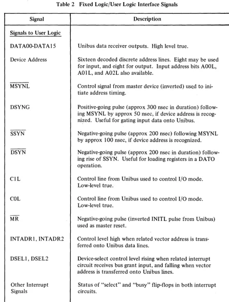
[image:5.614.78.528.44.655.2]USER LOGIC INTERFACE
Table 2 lists signals at the interface between fixed logic on the module and user interface logic. Connections are made at wire-wrap terminals on the module.
Table 2 Fixed Logic/User Logic Interface Signals
Signal Description
Signals to User Logic
DATAOO-DATAI5 Unibus data receiver outputs. High level true.
Device Address Sixteen decoded discrete address lines. Eight may be used
for input, and eight for output. Input address bits AOOL, AO 1 L, and A02L also available.
MSYNL Control signal from master device (inverted) use.d to
ini-tia te address timing.
DSYNG Positive-going pulse (approx 300 nsec in duration)
follow-ing MSYNL by approx 50 nsec, if device address is
recog-ni~ed. Useful for gating input data onto Unibus.
-SSYN Negative-going pulse (approx 200 nsec) following MSYNL
by approx 100 nsec, if device address is recognized.
- -
DSYN Negative-going pulse (approx 200 nsec in duration)follow-ing rise of SSYN. Useful for loadfollow-ing registers in a DATO operation.
CIL Control line from Unibus used to control I/O mode.
Low-level true.
COL Control line from Unibus used to control I/O mode.
Low-level true.
-MR Negative-going pulse (inverted INITL pulse from Unibus)
used as master reset.
INTADRI,INTADR2 Control level high when related vector address is
tranS-ferred onto Unibus data lines.
DSEL I, DSEL2 Device-select control level rising when related interrupt
circuit receives bus grant input, and falling when vector address is transferred onto Unibus lines.
Other Interrupt Status of "select" and "busy" flip-flops in both interrupt
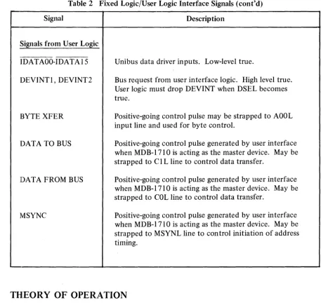
[image:6.618.89.536.124.713.2]Table 2 Fixed Logic/User Logic Interface Signals (cont'd)
Signal Description
Signals from User Logic
IDATAOO-IDATA15 Unibus data driver inputs. Low-level true.
DEVINT 1, DEVINT2 Bus request from user interface logic. High level true.
User logic must drop DEVINT when DSEL becomes true.
BYTE XFER Positive-going control pulse may be strapped to AOOL
input line and used for byte control.
DATA TO BUS Positive-going control pulse generated by user interface
when MDB-1710 is acting as the master device. May be strapped to C I L line to control data transfer.
DATA FROM BUS Positive-going control pulse generated by user interface
when MDB-1710 is acting as the master device. May be strapped to COL line to control data transfer.
MSYNC Positive-going control pulse generated by user interface
when MDB-1710 is acting as the master device. May be strapped to MSYNL line to control initiation of address timing.
TH[EORY
OF OPERATION
The logic diagram (Dwg. 40314) shows details of fixed logic furnished on the MDB-1710 module, and identifies· wire-wrap posts at which data, address, and control signals are term ina ted.
In general, logic on the module includes:
• data bus receivers and drivers,
• address selection logic,
• interrupt logic, and
• user interface logic designed and built on the module for the particular device application.
The following paragraphs describe the theory of operation of this logic.
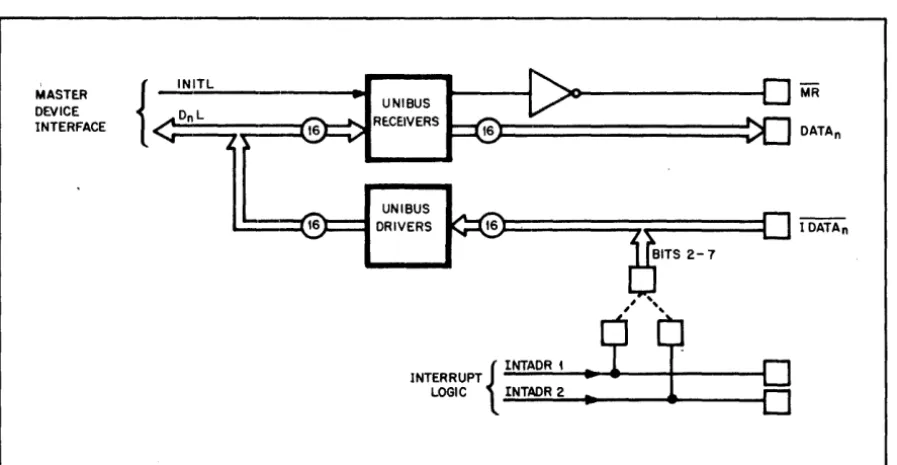
[image:7.617.80.538.55.490.2]DATA BUS
The 16-bit data word DnL at the Unibus data interface is received and made available (as DATAn) at wire-wrap posts for connection to user interface logic (see figure 2).
The I6-bit data word IDATAn from the user interface, connected at wire-wrap posts, is applied through drivers to the Unibus lines. In an interrupt sequence, either of two vector addresses (strapped at wire-wrap posts) is enabled onto lines IDATA02 through IDAT AD7
by a respective INTADRI or INTADR2 pulse.
ADDRESS SELECTION LOGIC
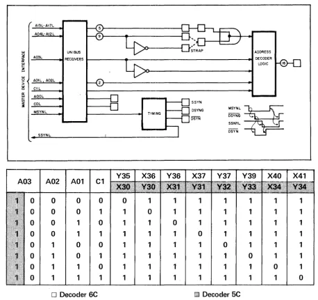
The address for the MDB-171 0 is selected by jumper connections at wire-wrap posts. Any address from 760000 through 777777 may be selected. The logic provides eight DATI addresses, and eight DATO addresses.
Sixteen sequential addresses are decoded, with the decoders enabled by address lines A04L through Al7L which control an open-collector wired-AND circuit (see figure 3).
Bus address lines Al3L through Al7L are hard-wired and all must be true at the input ter-minals to enable the wired-AND bus. Bus address lines A04L through AI2L each provide two complementary outputs, 'either of which may be strapped to the wired-AND bus. If the user-selected address bit is to be true, the bus receiver output is strapped to the wired-AND bus. If that bit is to be false, the inverter output is strapped to the bus.
Bus address line A03L is hardwired to select either of the two decoder chips (in location SC When A03L
=
"1 ", and location 6C when A03L=
"0"). Address bits AOIL and A02L, and control line C I L, are the least-significant bits of the address and are hard-wired to the decoders. Bit AOOL is not used at the decoders.MASTE.R { DEVICE
INTERFACE
C==;;::=::::(t
DATA n{
INTADR • INTERRUPT
LOGIC _IN_Ti_~_R_2--1 _ _ _ _ _ " " _ _ - - I
[image:8.618.93.542.457.689.2]At3L-AHL
A04L-AI2L
LU UNIBUS ADDRESS
~ A03L
RECEJVE~S DECODER
cr
LU LOGIC
I-~
LU
u A01L A02L
>
~ CIL
cr
LU AOOL
Iii SSYN
« COL ::I
MSYNL~
MSYNL DSYNG
DSYN DSYNG
SSNYL
DSYN • SSYNL
A02 AO' C,
0 0 0 0 0
, , , , , , ,
0 0 0
, ,
0, , , ,
, ,
0 0
,
'0, ,
0, , , ,
,
0 0
, , , , ,
0, ,
,
,
0
,
0 0,
,
, ,
0, ,
,
0
,
0, ,
,
, , ,
0,
,
0
,
,
0, , ,
,
, ,
0,
0
, , , , ,
,
, , , ,
0o
Decoder 6C !ill] Decoder 5CFigure 3 Address Selection Logic, Block Diagranl and Truth Table
Address selection logic also provides sync and loading signals. When the user address is decoded and the master device asserts MSYNL, the logic produces a series of timing signals DSYNG, SSYN, and DSYN. Term DSYN is a negative-going pulse approximately 200 nano-seconds in duration, and is useful for loading.ilata registers when the master device is per-forming a 'DATO operation. The signal SSYN is sent to the user interface and terminates DSYN. Simultaneous with SSYN, SSYNL is sent to the Unibus interface to indicate that the address has been acknowledged.
INTERRUPT LOGIC
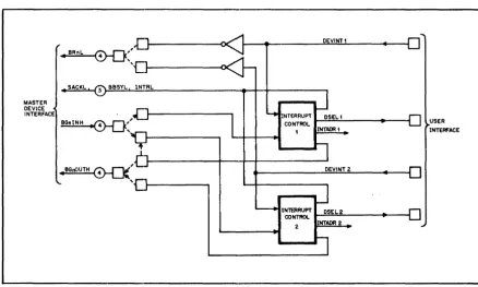
The MDB-1710 includes two separate sets of interrupt control logic, permitting the user to interrupt the PDP-II processor through two unique vector addresses. Wire-wrap facilities on the module are used to select any two vector addresses from 4 through 374. A logic" I" in the address is made by connecting a wire-wrap jumper. Logic "O's" need not be jump-ered. Either address is put onto the output data lines by a respective signal INTADRI or INTADR2.
[image:9.614.86.545.50.481.2]As shown in figure 4, bus request levels (BRnL) 4 through 7 are selected by wire-wrap jumpers.
An interrupt request is initiated when user interface logic puts a "I" (+3V) on a DEVINTn
line, dropping the level on a selected bus request line at the master device interface.
When the master device sends the bus grant signal (BGnINH), interrupt logic sends DSELn to the user interface which may then remove the DEVINTn signal. The interrupt acknow-ledge signal SACKL is sent to the master device when the bus grant signal is received.
The vector address is then sent to the master device when the bus becomes available; that is, BBSYL becomes false, raising INTADRI or INTADR2.
Other control signals BBSYL and INTRL sent to the master device reflect the state of either INTADRn line.
MASTER DEVICE INTERFACE
~-D<
• SACKL,
0
BBSYL, INTRL,
~:
,
~,
DEVINT I
INTERRUPT I,...!D~SE=.L
,!...-__
---1CONTROL
INTADR ,
DEVINT 2
l=;::r
~DS=E.::.:L 2=----_ _ ... ---42 INTADR 2
Figure 4 Interrupt Logic, Block Diagram
USER INTERFACE LOGIC
USER INTERFACE
User interface logic is designed for a specific application, and is built in the 40 integrated-circuit device locations provided on the module.
[image:10.615.91.529.255.518.2]JUJ\1PER CONNECTIONS
Certain jumper connections must be prepared on the module (other than the fixed logic/user logic connections) in order to configure the module for its application. Wire-wrap jumpers are to be prepared for both device address selection, and interrupt management and
addresses.
ADDRESS LOGIC
Unibus address bits A04L through A 12L must be connected to encode the device address. As shown on the logic diagram, for each bit an output may be taken from either the receiver output, or the output of an open-collector driver.
If a bit is to be true in the user-selected address, strap the receiver output to the wired-AND
circuit. If the bit is to be false, strap the driver output to the wired-AND circuit.
Bits Al3L through Al7L are hardwired and must be true (low) at the Unibus lines to enable the address decoder.
INTERRUPT LOGIC
Interrupt logic must be connected for each of the two vector interrupt circuits. Perform connections as follows:
Vector Addresses. The 6-bit vector address for each circuit is formed by jumpers at three rows of three wire-wrap posts on both sides of the I-C device in location BS.
To encode the vector address for either interrupt circuit, connect a jumper b.etween the out-put of a INTADR1 or INTADR2 inverter and the related IDATAn line (see logic diagram
40314). If both interrupts are to be used, wire addresses for both to IDATAn lines.
A jumper creates a logic" 1 ". A logic "0" is implied by lack of a jumper.
Inte~rrupt Management. Select the interrupt level for each interrupt circuit by connecting a jumper from terminal J or X to one of the four bus request (BRnL) terminals.
Unless both interrupts are to be at the same level, strap the selected bus grant input termi-nals to each interrupt circuit at terminal K or W.
If the interrupts are to be at the same level, strap the first-in-order interrupt circuit to a bus
grant input, and then strap the bus grant input of the second circuit to the bus grant output of the first. For example:
a. jumper terminal K to BG4INH, then
b. jumper terminal W to terminal M.
If the interrupt is to be extended through another controller, connect the bus grant output
from the appropriate interrupt circuit (terminal M or L) to the related bus grant output level (BGnOUTH).
USER LOGIC EXPANSION MODULE
The MDB-ll WW wire-wrap expansion module is available to expand user interface logic beyond the space allowed on the interface module. The MDB-ll WW is designed for cus-tom interface applications with Digital Equipment Corporation PDP-II and PDP-8 computers, and occupies a single quad slot. Two-level wire-wrap posts, installed on the component side of the board, permit h-inch board spacing within the computer mainframe.
The module accommodates combinations of as many as 70 dual-in-line ICs or sockets having 14, 16, 18, 22, 24, or 40 pins. IC positions are identified with a column and row identifi-cation. Two of the 10 colunlns (4 and 8) will handle ICs with from 14 to 40 pins, with up to three 40-pin ICs, or five 24-pin ICs, per column. Discrete components may be installed in these columns with components on 0.3-, 0.4- or 0.6-inch centers wherever no IC is
installed.
Sixteen of the 70 IC positions are dedicated for 14-pin sockets (positions Al through Al 0, and H3 through H8), and have prewired power and ground connections (pins 14 and 7, respectively). All the remaining positions will acconlll10date l6-pin devices, but the con-nection between pins 7 and 8 must be removed for any position to hold a l6-pin device.
Each position has power and ground decoupling pads to accommodate high-frequency disc capacitors. Decoupling pads next to column 10 will hold six low-frequency tantalum capaci-tors on O.4-inch centers.
BBSYL INT~l SA(K.l.. 8R5L BRR 8R7L 8G4INH 8G61NM
• 8(;7 INH
BG40UTH 8G60UTH 86?QUTI-I \ \ \ \ \ \ \\\ " \\\
"'~\r1
,'".
/ /14
/ /1,
III
;:L_ t;~~
!..""?""-""""",L.
r----r--
I/~----"T 5v
INTERRuPT CONTROL
3"
::
~E~:NTI."
Y21
X 25
DEVINT 2
RZ5 180
+ 5V
5SYNL AI?L AIGl AI5L AI4L Aloll AI2L AIOL A09L A08L A01L ~06L ~05L I\04L A03L ~02L "OIL CIL AOOL COL
ADDRESS AND DECODE
s---~ I
391 391 "'SYNC
I 391 3~r-2 _ _ _ _ _ _ _ _ -L_~~~
~ _ _ _ '_:.,l. 2.4. 14
21( RI.3
~
~~6--~---2K RI5
~
~~'-O~---2" RI2
~
~~4--~---2K "'8
~~-,_-,---2K FU4
~~-2~---2K RII
~
~~-6~---2' R6
~Y'-2-~---2K R7
~
~~.2--~---2t< R~
~
~~'O-~---2K R5
po-::.---+---< T I 7 DSYN~
D 7 6 6 5 8250 > 4 0
-ZK ;~ 5~
~-+ _______ --,-2 C 5C 4 ~
t -_ _ _ _ .!.:!I13 8 .3 ~
2~
'~
G~
t--+--4---y38 t----+---~x3S
2 C
~~---~L---JL--~138
+- ')11
CC2 0(2 GRD
- 15V
DATA I/O BuS
!C +-Sv 7~O~
D 15 L
014 L
DI.3 L
DIlL
DII L
DOSL DOSL D07L DOGL DOSL 004L D03L DOZL ~Oll DOOL IHITL
14 Ie I
+ 5v ~'t5'" PULLLJP
"'
IK SPARE RESISTORS
7406
:t=----+----'-INTAOR 2 1i-"----6.---INTAO~ I
+
5V~}
~+5V
---r---..,---I
+~ CS,7,9,1\ 1:l,15 .OUlf 12V- ... - -.... - - - - ! . - -GRD
LOGIC DIAGRAM, MDB-1710
C"'-'- - - / /) '\. i~ _ _ _ _ . _ _ ...
NOTE: UNLLSS OTHERWISE SPECIFIED
1. ASSl::NBLE PER QCALIFIE.D MANUFACTURING" :.\:-;i)!\RDS
2. SQUARE PADS I1JDICATE POSITI'JE SInE D" S.\P,iCITOR;; AND/OR CATHODE SIDE OF DIODes
3. FOR LIST OF '!ATERIAL SEE SEPARATE SHEET".
6~ DECOUPLING C;,PA,'ITORS AS ,U:QeIRLD
COMPo SIDE
ASSE·MBLY DWG.
f:1DB
SYSTEMS, INC.TITLE: MOB - 1710
f:1lJB
MOB SYSTEMS, INC.1995 N. Batavia St. Orange, California 92665 714-998-6900