UART TESTING UNDER BUILT-IN-SELF-TEST (BIST) USING VERILOG ON
FPGA
Dhwanit Arunkumar Juneja
Scholar, Department of Electrical and Electronics Engineering, California State University , Sacramento
Sacramento, California, United States Of America
---***---Abstract - The main aim of this research is to minimize the complications of VLSI chips which is increasing rapidly due to evolution in nanotechnology. Therefore, engineers are making their efforts to design a system with full testability reckoning the possibility of reduced product debacle and missed market opportunities. One of the most prevalent test techniques known as Built-In-Self-Test (BIST). BIST is highly effective and flexible that allows a system to test automatically itself with slightly higher system size. A BIST and Universal Asynchronous Receive/Transmit (UART) have the intent to initially satisfy specified testability requirements and to secondly generate the lowest-cost with better performance implementation. UART has been a vital data communication tool for a long time and is still extensively used. This paper focuses on the TRA (test response analyzer), the circuit of BIST, in this paper, in previous design TRA compares the results with ROM values, the proposed design implemented with simple MISR circuit. This paper emphases on the design of a UART chip with embedded BIST architecture using FPGA technology. The paper designates the glitches of VLSI testing followed by the performance of UART. Using this technique, the performance attained by BIST enabled UART architecture through is adequate to compensate for the extra hardware needed in BIST architecture. The technique can provide shorter test time paralleled to an externally applied test and allows the use of low-cost test equipment during all stages of production. The entire design will be performed using Verilog HDL and will try to minimize the power consumption and cell area
Key Words: BIST, UART, VLSI, LFSR, MISR, FPGA
1. INTRODUCTION
Technological evolution is a crucial factor for survival and growth. Due to physics-based simulation, advancement in silicon technology is rising. In this era of sub-micron technology, a single chip may contain millions of transistors. According to the Semiconductor Industry Association (SIA) estimates, the figure of transistors per chip and the local clock frequencies for high-performance microprocessors will continue to grow exponentially in the forthcoming future. The prediction is like Moore’s law, which points out that the number of transistors in an IC doubles every 18 months. The improvements, efficiency, and evolution ensure that future microprocessors and ICs will become even more complex. [2]
In this paper, my principal objective is to study the design and implement the BIST technique for Universal Asynchronous Receiver and Transmitter. Built-in Self-Test
(BIST), is the technique of building hardware and software topographies into integrated circuits to permit them to perform self-testing. BIST is a Design-for-Testability (DFT) system which makes the electrical testing of a chip easier, faster, more effective, and economical. The BIST has a wide range of applications, which varies as per the circuits. In this paper, the simulation result is compared with previous work and it has been seen that the result is promising and helps to reduce timing constraints and overall power dissipation. [1-3]Serial communication in this paper is vital to computers and permits them to communicate with low-speed peripheral devices, such as a keyboard, mouse, modems and so on. Universal Asynchronous Receiver and Transmitter is the most significant module required for serial communication. UART is an integrated circuit utilized for a change of serial data to parallel and vice versa. A BIST enabled UART has the objectives of initially to satisfy testability requirements and then to generate the highest performance implementation
2.BUILT-IN-SELF-TEST (BIST)
BIST is a design-for-testability technique that places the testing functions physically with the circuit under test (CUT), as illustrated in Figure 1. The elementary BIST design needs the addition of three hardware blocks to a digital circuit: a test pattern generator, a response analyzer, and a test controller. Examples of pattern generators are ROM with stored patterns, a counter, and a linear feedback shift register (LFSR). A response analyzer is a comparator with stored outputs or an LFSR utilized as a signature analyzer. It contracts and analyzes the test responses to determine the correctness of the CUT. A test control block is essential to trigger the test and examine the responses. Though, in general, some test-related functions can be implemented through a test controller circuit.
generated or stored on-chip, and the error signal indicates whether the chip is good or faulty.
Figure 1 BIST Architecture
Four primary parameters must be considered in developing a BIST methodology for embedded systems.
Fault coverage
Test set size
Hardware overhead
Performance overhead
BIST can be utilized for non-concurrent, on-line testing of the logic and memory parts of a framework. It can promptly be configured for event-triggered testing, in which case, the BIST control can be fixed to the system reset with the goal that testing happens amid system start-up or shutdown. BIST can likewise be intended for episodic testing with low liability latency. This requires consolidating a testing procedure into the CUT that ensures the detection of all target liabilities within a fixed time. On-line BIST is typically executed with the identical goals of comprehensive fault coverage and low fault expectancy. Henceforth, the test generation (TG) and response monitor (RM) are generally designed to assure coverage of precise fault models, least hardware overhead, and sensible set size. These goals are met by dissimilar methods in diverse parts of the system.[8]
TG and RM are frequently implemented by modest, counter-like circuits, particularly linear-feedback shift registers (LFSRs). The LFSR is just a shift register designed from usual flip-flops, with the outputs of flip-flops being fed back (modulo-2) to the shift register’s inputs. When used as a TG, an LFSR is set to cycle quickly through many of its states. Particularly in these states the order and choice depend on the design parameters of the LFSR which describe the test patterns. In this approach of procedure, an LFSR is seen as a foundation of (pseudo) random tests that are, in principle, appropriate to any fault and circuit types.
An LFSR can also serve as an RM by counting (in a special sense) the responses produced by the tests. An LFSR RM’s final contents after applying a sequence of test responses
form a fault signature, which can be compared to a known or generated good signature, to see if a fault is present. Affirming that the fault coverage is adequately high, and the figure of tests is sufficiently low are the key problems with random BIST approaches. Two general methodologies have been proposed to save the cost favorable circumstances of LFSRs while making the produced test succession a lot shorter. Test points can be embedded into the CUT to improve controllability and observability; nevertheless, they can also result in performance loss. Instead, some determinism can be presented into the generated test sequence, for example, by inserting specific “seed” tests that are known to detect hard faults.
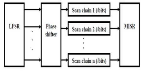
A usual BIST design by means of LFSR is publicized in Figure 2. Since the yield patterns of the LFSR are time-shifted and rehashed, they become interrelated; this lessens the
Figure 2 A generic BIST architecture based on an LFSR & a MISR
Efficiency of the fault detection. Along these lines, a phase shifter (a system of XOR gates) is frequently used to decorrelate the output patterns of the LFSR. The reply of the CUT is typically compacted by a multiple input shift register (MISR) to a small signature, which is compared with a known fault-free signature to regulate whether the CUT is defective.
3. BIST PATTERN GENERATION USING LINER FEEDBACK SHIFT REGISTER (LFSR)
[image:2.595.325.552.311.425.2]pseudo-random binary sequence where the bits look to be pseudo-random in the partial intellect, but they are in some way repeatable.
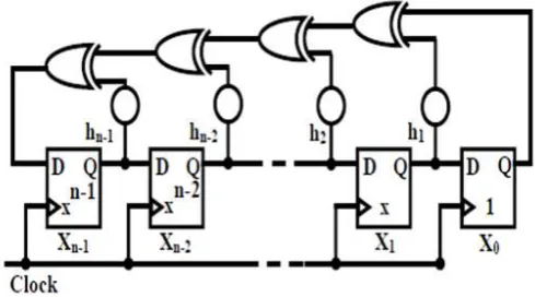
The LFSR (Linear feedback shift register) is a pattern generator which is usually utilized to generate irregular pattern sequence. In contrast with other procedures, BIST may need a long test period and demand valuation of fault coverage by long test period and demand valuation of fault coverage by fault simulation. LFSR reseeding might be stationary, that is LFSR halts generating patterns while loading seeds, or dynamic, for example, test generation and seed loading can advance at the same time.
[image:3.595.311.551.286.434.2]The figure represents the method we utilized to generate the random pattern generator using XOR linear feedback shift register. There are n flip-flops (Xn-1, Xn-2,…,X0) and so this architecture to generate random patterns is termed as n-stage LFSR. It might be a near-exhaustive test pattern generator as it cycles through 2n-1 states excluding all 0 states. This is known as a maximal length LFSR. It generally generates patterns at high speed with fewer hardware components. It is generally used for random pattern generation, error correction, and counters.
Figure 3 n-stage LFSR implementation with actual digital circuit
4. SHIFT REGISTER
One of the two primary portions of an LFSR is the shift register (the other being the feedback function). A shift register is a device whose recognizing function is to shift its contents into nearby positions inside the register or, because of the location on the end, out of the register. The situation on the other end is left unfilled except some new data is shifted into the register.
The data of a shift register are typically thought of as being binary, that is, ones and zeroes. If a shift register comprises the bit pattern 1101, a shift (to the right in this case) would outcome in the data being 0110; another shift yields 0011. Subsequently, two more shifts, things incline to get tedious since the shift register will never contain something besides zeroes.
Two usages for a shift register are
Conversion between parallel and serial data.
Delay a serial bit stream.
The conversion function can go anyway -- fill the shift register locations all at once (parallel) and then shift them out (serial) or shift the data into the register bit by bit (serial) and then recite the contents after the register is full (parallel). The delay function basically shifts the bits from one end of the shift register to the other, as long as a delay is equal to the length of the shift register.
[image:3.595.45.290.377.513.2]5. TEST PATTERN GENERATOR (TPG)
Figure 4 Design of TPG
Implementing the TPG for UART design, this TPG consists of modules like CA (Cellular Automata) LFSR and PISO. LFSR generate the random values to feed into the UART transmitter input. When the TRG signal goes high then only a new value is generated in the LFSR. This LFSR will generate (2n-1) different pseudo-random patterns. When the TRG signal is high, a new data is generated at LFSR which is fed parallelly into the transmitter section and this data is also given to PISO module and its serial output is fed into the receiver section of UART.
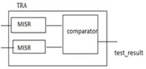
6. MULTIPLE INPUT SIGNATURE REGISTER (MISR) AND TEST RESPONSE ANALYSIS (TRA)
TRA module consists of MISR and compactor. MISR captures the output of UART and gives the final signature value to the compactor, where it compares the final signature value to reference golden signature value after clock cycles. If they are equal there is no fault, if not there is a fault. Compactor result is 2-bits, if the result is there is no fault in TX and RX, if 01 then uart tx fault, if 10 rx fault.
Here, when the trg signal goes high, a new data is obtained from the LFSR which is fed in parallel to the input of the transmitter. After a specific number of clock cycles, similar data is found at the output of the transmitter as sequential data. This serial data is moved in the SIPO of the comparator and this is the tx_out data. This tx_out is fed to MISR, and it computes the signature value, after 256 random values we analyze the concluding signature value of MISR and reference Golden Signature value.
[image:4.595.324.541.98.252.2]Based on the assessment, the outcome (rslt) is generated. If the both MISR final sign and golden signature are similar then test_result=1, else test_result=0. As the receiver delivers 8-bit parallel output, a SIPO is not required in this circumstance. The output from the receiver “rx_data” is right away given to MISR, it analyses the signature value, and after 256 random values, we relate the final signature value of MISR and reference Golden signature value.
Figure 5 Design of TRA
7. SERIAL-IN, PARALLEL-OUT (SIPO)
[image:4.595.35.277.429.543.2]This arrangement allows conversion from serial to parallel format. Data is input serially, as described in the figure 6. The minute data is fed at the input, it may be moreover read off at each output concurrently, or it can be shifted out and swapped.
Figure 6 SIPO Shift Register
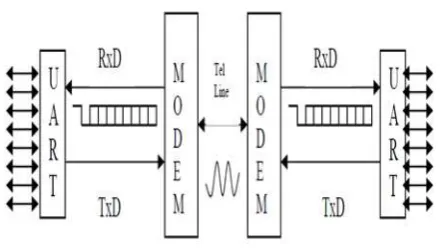
8. UNIVERSAL ASYNCHRONOUS RECEIVER AND TRANSMITTER (UART)
UART is a part of computer hardware that translates data between parallel and serial forms. Generally, serial data is transmitted using its serial port, which is the universal part of a computer. It is a connector where the serial line is attached and connected to a peripheral device such as a mouse, modem, printer and even to other computers. In contrast to parallel communication, these peripheral devices communicate using a serial bit stream protocol (data is sent one bit at a time). The serial port is typically linked to UART, an integrated circuit which performs the conversion between serial and parallel data.
Bit transmission shown in figure 7 signifies how the UART does its communication by receiving a byte of parallel data and then it translates it to a sequence of voltage to represent 0s and 1s on a single wire(successively). To transmit data on a telephone line, the data must be converted from 0s and 1s to the analog signal. This translation is completed by a
peripheral device called a modem
(modulator/demodulator). The modem transmits the signal on the single wire and converts it to sounds. On other side, the modem translates the sound back to voltages and another.
Figure 7 Serial Data Transmission
9. DESIGNOFUART
The structure of UART is as shown in Figure 8, consists of Transmitter part and Receiver part, rather we can say consists of 3 units, transmitter circuit, a receiver circuit and Control/Status Registers.
The UART block consists of various I/O signals for both the Transmitter and Receiver section and it operates as per the input signal fed to the entire system and carry out the operation of Serial Transmission and exchange of data between a CPU and other peripheral devices. [1]
Figure 8 Structure of UART Block
The UART block consists of various I/O signals for both the Transmitter and Receiver section and it operates as per the input signal fed to the entire system and carry out the operation of Serial Transmission and exchange of data between a CPU and other peripheral devices. [1]
9.1 Design of UART Transmitter
Transmitter unit contains an output register, transmitter control logic, and a transmitter buffer register. It has few I/O operations pins to perform its operation and they are: Serial
[image:5.595.309.555.251.431.2]data O/P, ACK, RST, CLK bar, TxRDY is O/P pin which indicates that the TX is ready to transmit data, TxE is O/P pin which indicates that the TX has no data in its output register to transmit.
[image:5.595.38.292.431.628.2]Figure 9 is of UART Transmitter. The data is loaded from Data Bus into TBR through Internal Data Bus. Then from TBR to output register based on the signals generated by TX control logic. The size of the output register is taken in such a way that, it should accommodate the START and STOP bits along with the data bits which are loaded from Data Bus. The Data loaded into output register has the format of START-DATA-STOP bits which is a standard data format.
Figure 9 UART Transmitter Unit
Correspondingly, the data in the output register will keep updating with 0’s; will be filled with 0’s, after transmission of the complete data packet. [1]
9.2 Design of UART Receiver
Figure 10 shows the architecture of the UART receiver section. It contains various blocks to perform its operation and they are:
Input Register: It is a serial input and serial output register which consists of 8 D flip-flops to store and shift 8-bit input data. The input data of the register is the serially transmitted data from Transmitter and fed to the receiver.
Receiver Buffer Register: It is an 8-bit serial in the parallel out register. The data of i/p register is shifted and enters bit by bit in every rising clock edge in Receiver Buffer Register. After entering 8-bit data, the buffer gets full.
Receiver Control Logic: This block decides when data is to be taken inside the receiver and when data is to be sent to the peripheral device.
want data from the receiver, but the receiver buffer register is full then any data cannot be taken inside the Receiver section and if any data arrives then data should be discarded. When the peripheral device wants data from the receiver, but the receiver buffer register is not full then no data is sent to the peripheral and data is taken in Receiver buffer from input register. Now if the peripheral device does not want data from the receiver buffer register is not full then data is taken inside Receiver buffer from input register with each clock pulse rising but data is not sent to the peripheral.[1]
Figure 10 UART Receiver
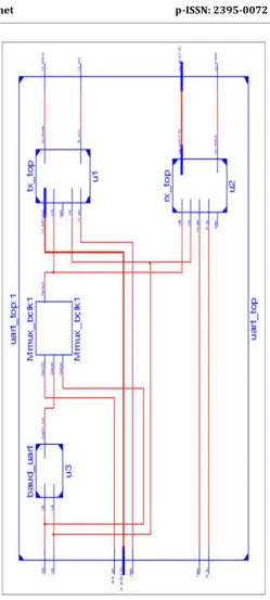
10. TOP LEVEL MODULE
Figure 11 Top Module UART
Figure 11 shows a top-level module of UART. The inputs are TxData_in (transmitter input), clk (clock), rst (Reset), Test_En (Teste Enable), Rx_in (Receiver Input), Golden_sign. The output from the top-level modules is Rx_Data_out (Receiver output signal), Test_result, Rx_done, Tx_done, Tx_out.
Figure 12 UART Top
RTL Schematic
[image:6.595.37.284.240.638.2]Figure 13 RTL Schematic
[image:7.595.307.556.136.331.2]11. Simulation Results
Figure 14 shows the simulation result of the LFSR module. The random data is generated at port q at every positive edge of the clock signal. When rst is high the trg_out and trg will be low and both the signals will be high when rst is low.
Figure 14 Simulation of LFSR
Figure 15 shows the simulation result of Transmitter module. The input pins are tx_in, clk, rst and oen whereas output pins are tx_out and tx_done.
Figure 15 Simulation of Transmitter
Figure 16 shows the simulation result of the Receiver module. The input pins are rx_in, clk, rst and wen whereas output pins are rx_out and rx_done.
Figure 16 Simulation of Receiver
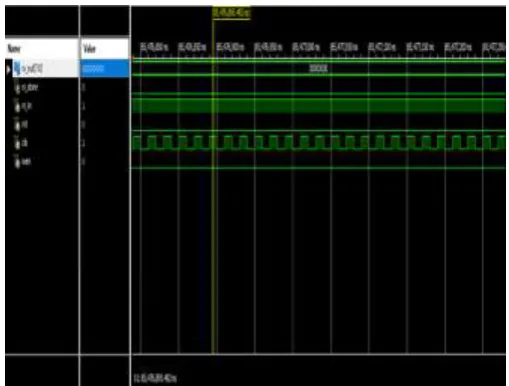
[image:7.595.306.561.407.600.2] [image:7.595.36.290.529.742.2]Figure 17 Simulation of BIST
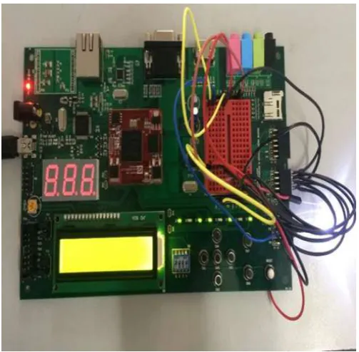
12. IMPLEMENTATION ON SPARTAN-6 FPGA BOARD
[image:8.595.33.302.82.307.2]When the input is “10110101”, only the corresponding light emitting diodes light up. This is shown in figure 18 and when the input is “11110101”, only the corresponding light emitting diodes light up is shown in figure 19.
Figure 18 Generating output with 10110101
Thus, whatever data is applied at the input is observed at the output. These results successfully validate the operation of the UART.
Figure 19 Generating output with 11110101
13. SYNTHESIS REPORT
Timing Summary:
---
Speed Grade: -3
Minimum period: 5.093ns (Maximum Frequency: 196.357MHz)
Minimum input arrival time before clock: 4.628ns
Maximum output required time after clock: 4.761ns
Maximum combinational path delay: 6.069ns
Default path analysis
Total number of paths / destination ports: 17 / 9
---
Delay: 6.718ns (Levels of Logic = 3)
---
Total 6.718ns (4.475ns logic, 2.243ns route)
(66.6% logic, 33.4% route)
Total REAL time to Xst completion: 15.00 secs
Total CPU time to Xst completion: 14.61 secs
[image:8.595.36.288.406.653.2]ADVANTAGES
Lower cost of the test, since the need for external electrical testing using an ATE, will be reduced.
Shorter test times if the BIST can be designed to test more structures in parallel.
Ability to complete tests externally in the production electrical testing environment.
Electrical injection of pulses does not cause any damage to the Semiconductor material.
May be used to injecting pulses simultaneously at multiple nodes to test for multi-bit upsets.
Electrical injection of pulses can be controlled precisely or can be made completely random as well, depending on the circuit and application for which the testing is done.
It incurs the minimal cost and testing time requirements.
DISADVANTAGES
Additional space is required on the chip to implement the BIST functionality.
The BIST functionality must be incorporated precisely so that it does not interfere with the primary purpose of the chip. This requires additional efforts on the designers’ part.
CONCLUSION
The main objective of this design is to implement a UART under BIST, capable of transmitting and receiving eight-bit data has been successfully accomplished. Simulations were performed on Xilinx ISE design suite for various inputs and the outputs were observed. The design was also implemented on Spartan-6 FPGA. BIST (Built in Self Testing) was executed with the help of a pseudo-random pattern generator. The output of this pattern generator was fed to the receiver of UART. The input fed by the user at the transmitter of UART was compared with this pattern at the UART’s receiver. If there was not an exact match of data, an interrupt signal was generated in the form of a led lighting on the board. With the implementation of BIST technique, expensive testing procedures starting from circuit or logic level to field level testing are minimized. The LFSR replaces the function of the external tester features such as a test pattern generator by automatically generating pseudo-random patterns to give maximum fault coverage to the UART module. The reduction in testing cost leads to a reduction of overall production cost as well.
REFERENCES
[1] Tapas Tewary, Atanu Sen “A novel approach to realize Built-in-self-test(BIST) enabled UART using VHDL”, IEEE 2014 First International Conference on Automation, Control, Energy and Systems (ACES)
[2] Mohd Yamani Idna Idris, Mashkuri Yaacob, Zaidi Razak, “A VHDL Implementation of UART Design with BIST capability”
[3] Dr. T.V.S.P. Gupta, Y. Kumari,M.Asok Kumar “UART realization with BIST architecture using VHDL” International Journal of Engineering Research and Applications (IJERA) ISSN: 2248-9622 www.ijera.com Vol. 3, Issue 1, January -February 2013, pp.636-640
[4] P. J. Anderson , “The designer’s guide to VHDL” , Morgan Kaufman ,2nd edition, 2002.
[5] Neil H.E. Weste, Kim Haase, David Harris , A. Banerjee , “CMOS VLSI Design: A circuits and Systems Perspective”, Pearson Education.
[6] K. Zarrineh, and S. J. Upadhyaya, “On programmable memory built-in-self-test architectures”, Design, Automation and Test in Europe Conference and Exhibition 1999. Proceedings , 1999, pp. 708 -713
[7] Suyash Pradhan, “Implementation of UART with BIST technique in FPGA”
[8] Version 2 IEEE IIT, Kharagpur “Built-in-Self-Test for Embedded Systems,” IIT Kharagpur
[9] Prof N. Patel, V. Patel, and V. Patel, “VHDL Implementation of Uart with status register,” Sarvajanik College of Engineering and Technology, Gujarat, India