Prepared for submission to JINST
Ionization Electron Signal Processing
in Single Phase LArTPCs
II. Data/Simulation Comparison
and Performance in MicroBooNE
MicroBooNE Collaboration
C. Adamsi R. Anj J. Anthonyc J. Asaadiaa M. AugeraS. Balasubramanianee B. Ballerh C. BarnespG. Barrs M. Bassb F. Baybb A. Bhatx K. Bhattacharyat
M. Bishaib A. Blakel T. Boltonk L. CamillerigD. Caratellig I. Caro Terrazasf R. Carro R. Castillo Fernandezh F. CavannahG. CeratihH. Chenb Y. Chena E. Churcht
D. CiancigE. Coheny G. H. Collino J. M. ConradoM. Converyw L. Cooper-Troendleee J. I. Crespo-Anadóng M. Del Tuttos D. DevittlA. DiazoM. Dolceb S. Dytmanu
B. Eberlyw A. Ereditatoa L. Escudero Sanchezc J. Esquivelx J. J Evansn
A. A. FadeevagB. T. Flemingee W. Foremand A. P. FurmanskinD. Garcia-Gamezn G. T. GarveymV. GentygD. Goeldia S. Gollapinniz E. GramellinieeH. Greenleeh R. Grossoe R. Guenettei P. GuzowskinA. Hackenburgee P. Hamiltonx O. Heno J. HewesnC. HillnJ. HodG. A. Horton-Smithk A. HourlieroE.-C. HuangmC. Jamesh J. Jan de VriescL. Jiangu R. A. Johnsone J. Joshib H. JostleinhY.-J. Jwag
D. KalekogG. KaragiorgigW. KetchumhB. Kirbyb M. KirbyhT. Kobilarcikh I. Kresloa Y. Lib A. Listerl B. R. Littlejohnj S. LockwitzhD. Lorcaa W. C. LouismM. Luethia B. Lundbergh X. LuoeeA. MarchionnihS. MarcoccihC. MarianiddJ. Marshallc D. A. Martinez Caicedoj A. Mastbaumd V. Meddagek T. MettleraT. Miceliq G. B. Millsm A. Moganz J. Moono M. Mooneyf C. D. MoorehJ. Mousseaup M. MurphyddR. MurrellsnD. Naplesu P. Nienaberv J. Nowakl O. Palamarah V. PandeyddV. Paoloneu A. Papadopoulouo V. Papavassiliouq S. F. Pateq
Z. Pavlovich E. Piasetzkyy D. PorzionG. Pulliamx X. QianbJ. L. RaafhV. Radekab A. Rafiquek L. Rochesterw M. Ross-LonergangC. Rudolf von Rohra B. Russellee D. W. SchmitzdA. Schukrafth W. SeligmangM. H. Shaevitzg J. SinclairaA. Smithc E. L. SniderhM. Soderbergx S. Söldner-RemboldnS. R. Soletis,i P. Spentzourish J. SpitzpJ. St. Johne,h T. StrausshK. SuttongS. Sword-Fehlbergq A. M. Szelcn N. Taggr W. Tangz K. Teraow M. ThomsoncM. ToupshY.-T. Tsaiw S. Tufanliee T. Usherw W. Van De Pontseeles,i R. G. Van de WatermB. Virenb M. Webera H. Weib D. A. Wickremasingheu K. Wiermant Z. Williamsaa S. Wolbersh T. Wongjiradcc K. WoodruffqT. YanghG. Yarbroughz L. E. YatesoB. YubG. P. ZellerhJ. Zennamod C. Zhangb
aUniversität Bern, Bern CH-3012, Switzerland
bBrookhaven National Laboratory (BNL), Upton, NY, 11973, USA
cUniversity of Cambridge, Cambridge CB3 0HE, United Kingdom
dUniversity of Chicago, Chicago, IL, 60637, USA
eUniversity of Cincinnati, Cincinnati, OH, 45221, USA
fColorado State University, Fort Collins, CO, 80523, USA
gColumbia University, New York, NY, 10027, USA
hFermi National Accelerator Laboratory (FNAL), Batavia, IL 60510, USA
iHarvard University, Cambridge, MA 02138, USA
jIllinois Institute of Technology (IIT), Chicago, IL 60616, USA
kKansas State University (KSU), Manhattan, KS, 66506, USA
lLancaster University, Lancaster LA1 4YW, United Kingdom
mLos Alamos National Laboratory (LANL), Los Alamos, NM, 87545, USA
nThe University of Manchester, Manchester M13 9PL, United Kingdom
oMassachusetts Institute of Technology (MIT), Cambridge, MA, 02139, USA
pUniversity of Michigan, Ann Arbor, MI, 48109, USA
qNew Mexico State University (NMSU), Las Cruces, NM, 88003, USA
rOtterbein University, Westerville, OH, 43081, USA
sUniversity of Oxford, Oxford OX1 3RH, United Kingdom
tPacific Northwest National Laboratory (PNNL), Richland, WA, 99352, USA
uUniversity of Pittsburgh, Pittsburgh, PA, 15260, USA
vSaint Mary’s University of Minnesota, Winona, MN, 55987, USA
wSLAC National Accelerator Laboratory, Menlo Park, CA, 94025, USA
xSyracuse University, Syracuse, NY, 13244, USA
yTel Aviv University, Tel Aviv, Israel, 69978
zUniversity of Tennessee, Knoxville, TN, 37996, USA
aaUniversity of Texas, Arlington, TX, 76019, USA
bbTUBITAK Space Technologies Research Institute, METU Campus, TR-06800, Ankara, Turkey
ccTufts University, Medford, MA, 02155, USA
ddCenter for Neutrino Physics, Virginia Tech, Blacksburg, VA, 24061, USA
eeYale University, New Haven, CT, 06520, USA
Abstract: The single-phase liquid argon time projection chamber (LArTPC) provides a large amount of detailed information in the form of fine-grained drifted ionization charge from particle traces. To fully utilize this information, the deposited charge must be accurately extracted from the raw digitized waveforms via a robust signal processing chain. Enabled by the ultra-low noise levels associated with cryogenic electronics in the MicroBooNE detector, the precise extraction of ioniza-tion charge from the inducioniza-tion wire planes in a single-phase LArTPC is qualitatively demonstrated on MicroBooNE data with event display images, and quantitatively demonstrated via waveform-level and track-waveform-level metrics. Improved performance of induction plane calorimetry is demonstrated through the agreement of extracted ionization charge measurements across different wire planes for various event topologies. In addition to the comprehensive waveform-level comparison of data and simulation, a calibration of the cryogenic electronics response is presented and solutions to various MicroBooNE-specific TPC issues are discussed. This work presents an important improvement in LArTPC signal processing, the foundation of reconstruction and therefore physics analyses in MicroBooNE.
Contents
1 Introduction 2
1.1 Review of signal processing concepts 4
2 Calibration of TPC cold electronics response function 6
2.1 MicroBooNE TPC cold electronics calibration system 6
2.2 Electronics response parameterization 8
2.3 Stability of electronics response 12
2.4 Validation of electronics response correction 12
3 Validation of field response function simulation with data 14
3.1 Response extraction methodology 16
3.2 Response in normal region 19
3.3 Response in shorted-wire regions 21
3.4 Signal processing for shorted-wire regions 25
4 Cleaning and filtering of data events 27
4.1 Removal of PMT-induced TPC signals 27
4.2 Correction of ADC bit shifts 29
4.3 Handling purity-monitor-induced burst noise and cathode burst events 32
5 Evaluation of signal processing performance on MicroBooNE data 36
5.1 Event displays 38
5.2 Demonstration of cross-plane charge matching 40
1 Introduction
MicroBooNE [1,2], or the Micro Booster Neutrino Experiment, is located at Fermilab in Batavia,
Illinois, and has the goal of addressing the low-energy electron-neutrino-like excess observed at
MiniBooNE [3] on the same beam line (the Booster Neutrino Beam, or BNB). In order to address
this anomaly, the experiment utilizes a different detector technology, a liquid argon time projection
chamber (LArTPC). The LArTPC [4–7] provides fine-grained spatial resolution and an excellent
calorimetric capability that allows for discrimination between electrons and photons in the active
volume of the TPC [8]. This discrimination power is key to the success of the MicroBooNE physics
program, as it allows one to identify the photon backgrounds which complicate the MiniBooNE electron appearance search.
The MicroBooNE LArTPC, illustrated in figure 1, utilizes three wire planes at the anode
to obtain signals from drifting ionization electrons produced from neutrino interactions within the active volume of the detector. Drifting ionization electrons first pass by the two induction planes (the “U plane” and “V plane”), inducing signals on the wires, and are finally collected on the collection plane (the “Y plane”). The drift electric field is approximately 273 V/cm and is maintained by a cathode held at -70 kV as well as a field cage that surrounds the LArTPC active volume and gradually steps down the voltage toward the anode plane via a resistor chain. The three wire planes are biased at specific voltages (-110 V, 0 V, and +230 V for the U plane, V plane, and Y plane, respectively) to ensure complete transparency for drifting ionization electrons, allowing for all ionization electrons to reach the third (collection) wire plane without being collected by one of the first two (induction) wire planes. Bipolar signals are produced on the induction planes and largely unipolar signals are produced on the collection plane.
One primary asset of the LArTPC technology is its capability of discriminating between electrons and photons in the detector. This is strongly desired in accelerator neutrino experiments as photons are often backgrounds to searches for electron neutrino appearance. Photons that convert into an electron-positron pair within the liquid argon can be indentified as having roughly double
the value of dE/dx compared to a single electron, measured using the calorimetric information
(recovered from the charge measured at the TPC wires) of the track-like beginning of the particle signature in the detector. In order to make use of the electron versus photon discrimination capability of the LArTPC technology, it is necessary to first demonstrate the ability to extract charge precisely from these signals on the TPC wires; both imaging and calorimetry in the TPC active volume depend on this precise charge extraction.
Three elements come into play for signal formation on TPC wires: i) the distribution of the ionization charge cloud produced by charged particles traveling through the TPC; ii) the field response describing charge collection and induction on the TPC wires as ionization electrons drift through the wire planes; and iii) the electronics response characterizing the amplification and shaping of the induced current on the TPC wire in the front-end electronics. A detailed simulation of each of these effects is required to realistically simulate particle interactions within
the MicroBooNE detector for comparison with data. GEANT4 [10] is used to simulate the energy
deposition of charged particles traveling through the liquid argon and LArSoft [11] is utilized to
simulate ionization charge recombination, transport, and diffusion. For the wire field response and
Cathode Plane
Edrift
U V Y
Liquid Argon TPC
Y wire plane waveforms
V wire plane waveforms Sense Wires
t
Incoming Neutr ino
[image:6.595.113.465.123.380.2]Charged Particles
Figure 1: Illustration of signal formation in the MicroBooNE three-plane LArTPC, depicting the
V plane (second induction plane) and Y plane (collection plane) TPC wire signals on the right of the image [9].
The electronics response shape is taken from a parametrization of the expected response of the front-end electronics at a given gain and peaking time, while the wire field response is simulated
using Garfield [13]. This wire field response simulation includes a dependence on the impact
parameter of the ionization electron drift with respect to the wires, as well as the charge induction on wires both close to and far from the drifting ionization electrons.
After the employment of software noise filtering techniques to eliminate excess noise from
external sources [14], a robust signal processing chain [12,15] is required to extract the number of
drifting ionization electrons passing through each wire plane. It is necessary to validate this signal processing chain with data from the MicroBooNE LArTPC in order to evaluate the performance of drifted charge extraction from the TPC wires. This work describes this validation, as well as the
validation of the TPC signal simulation described in Ref. [12], by making comparisons between
MicroBooNE data and simulation. In addition, the performance of charge-matching across the three wire planes of the MicroBooNE LArTPC is illustrated in this work.This charge-matching
can be utilized in novel imaging techniques [16] that take advantage of local cross-plane charge
interactions.
This article is organized as follows. First, in the remainder of the introduction, a brief review
of signal processing concepts referenced throughout this work is presented. In section 2 the
calibration of the electronics response function on a channel-by-channel basis, which enables a
uniform electronics response across all TPC channels, is described. Next, in section3, a comparison
of data and simulation at the waveform level is carried out, characterizing the capability of the ionization signal simulation to reproduce the response of the TPC wires and the electronics to drifted ionization charge. This section also includes discussion of a method used to account for the modified response function in the shorted regions of the detector, where a group of channels in the collection plane (Y plane) are shorted to a non-standard bias voltage. Special considerations
necessary to employ the signal processing chain discussed in Ref. [12] on data are presented
in section 4, including the addressing of electronics/noise issues that complement the studies
highlighted in Ref. [14]. Results of applying the signal processing chain on MicroBooNE data
are shown in section 5, including the characterization of its performance on events in data and
a demonstration of the precise extraction of charge information from the induction planes of a
LArTPC, which has previously been shown to be feasible [17]. Emphasized in this section is the
matching of charge across the three planes of the MicroBooNE LArTPC. Finally, a summary of the
investigations carried out in this work, along with their significance, is presented in section6.
1.1 Review of signal processing concepts
A number of fundamental signal processing concepts are referenced throughout this article that are worth discussing briefly as background information. For a more complete discussion of LArTPC
signal processing concepts and methodology, see Ref. [12].
The deconvolution technique is used to extract charge information from LArTPC waveform
data, and has been utilized previously in the data analysis of other LArTPC experiments [15,
18]. More advanced deconvolution techniques have been explored in MicroBooNE [12] and are
validated with data events in this work. In brief, the deconvolution is used to extract the original
ionization charge signalS(t)from the measured signal M(t0). The measured signal is modeled as
the convolution of the original signalS(t)and a known detector response functionR(t0−t):
M(t0)=
∫ ∞
−∞
R(t0−t) ·S(t)dt. (1.1)
This “full” detector response R(t0−t) includes both the wire field response and the electronics
response, and can be either simulated or estimated from data using an independent calibration
sample (see section 2 and section3). One can transform Eq.1.1 into the frequency domain by
applying a Fourier transformation, yielding M(ω) = R(ω) ·S(ω), whereω is in units of angular
frequency. The original signal in the frequency domain S(ω) can be found by rearranging this
equation:
S(ω)= M(ω)
R(ω). (1.2)
This solution is extended to account for additional detector and electronics noise contributions
through the introduction of a low-pass filter functionF(ω), yielding
S(ω)= M(ω)
The purpose of the filter function is to attenuate problematic high-frequency noise that is amplified by the deconvolution procedure (division of noise by the response function at frequencies where the signal response is very small).
The above deconvolution prescription is known as the “one-dimensional (1D) deconvolution” in the sense that a fast Fourier transform (FFT) is carried out in the time dimension only. This procedure assumes the induced current on each sense wire is independent of the topology of
the charge distribution creating the signals on the wires. However, as described in Ref. [12],
the induced current on the sense wire receives additional topology-dependent contributions from ionization charge drifting past adjacent wires at roughly the same time. Accounting for these additional contributions and assuming the field response strength between wires is approximately
constant allows Eq. (1.1) to be generalized as
Mi(t0)= ∫ ∞
−∞
(...+R1(t0−t) ·Si−1(t)+R0(t0−t) ·Si(t)+R1(t0−t) ·Si+1(t)+...) ·dt, (1.4)
where Mi represents the measured signal from wirei. Si−1, Si, andSi+1represent the real signal
inside the boundaries of wireiand its adjacent intra-plane neighbors. R0andR1are the average full
response functions for ionization charge passing through the wire region of interest and adjacent wire regions respectively.
Converting this equation into the frequency domain by applying a Fourier transform yields
Mi(ω)= ...+R1(ω) ·Si−1(ω)+R0(ω) ·Si(ω)+R1(ω) ·Si+1(ω)+..., (1.5)
which can be written in matrix notation as
© «
M1(ω) M2(ω)
... Mn−1(ω)
Mn(ω) ª ® ® ® ® ® ® ® ¬ = © «
R0(ω) R1(ω) . . . Rn−2(ω) Rn−1(ω) R1(ω) R0(ω) . . . Rn−3(ω) Rn−2(ω)
... ... . . . ... ...
Rn−2(ω) Rn−3(ω) . . . R0(ω) R1(ω) Rn−1(ω) Rn−2(ω) . . . R1(ω) R0(ω)
ª ® ® ® ® ® ® ® ¬ · © « S1(ω) S2(ω)
... Sn−1(ω)
Sn(ω) ª ® ® ® ® ® ® ® ¬ . (1.6)
Inverting the matrix R via application of Fourier transforms allows for the determination of the
original signal vector S. This “two-dimensional (2D) deconvolution” yields a more accurate
recovery of the ionization electron distribution using the known detector response in both the time and wire dimensions.
baseline of the signal contained in the ROI is defined by an interpolation using the signal sidebands, and a Gaussian filter is utilized to extract the ionization charge. This procedure is discussed in more detail in Ref. [12].
2 Calibration of TPC cold electronics response function
Each wire is individually instrumented by an electronic circuit that amplifies and shapes its current
signals [19]. These pre-amplifiers are implemented as application-specific integrated circuits
(ASICs) and are operated at cryogenic temperature inside the liquid argon cryostat in order to reduce electronic noise and simplify detector cabling. The amplified analog voltage signals are routed out of the detector cryostat, amplified again by intermediate warm electronics and digitized
at 2 MHz by 12-bit analog to digital converters (ADCs) [9].
Cryogenic (cold) pre-amplifying electronics are a crucial element of the MicroBooNE LArTPC as the reduced electronic noise during cryogenic operation compensates for the absence of ionization charge amplification within the liquid argon. Charge measurements made with induction wire signals especially require low electronic noise due to the relatively small currents induced on the
wires by the drifting ionization charge [20]. Excellent cold electronic noise performance was
observed in the MicroBooNE detector following the start of regular operation, with an equivalent
noise charge (ENC) measured to be less than or equal to 400 e− for the majority of channels
compared to an expected signal size of ∼17000 e− from minimum ionizing particles traveling
parallel to the wire plane and perpendicular to the wire direction [14].
Each individual cold electronics ASIC channel can be configured to use one of four different
gain settings (4.7, 7.8, 14 and 25 mV/fC) and peaking time settings (0.5, 1, 2 and 3 µs). During
normal operation, MicroBooNE uses the 14 mV/fC gain setting and 2 µs peaking time, which
satisfies the Nyquist criterion [21] for 2 MHz digital sampling. The output baseline voltage is set
to∼200 mV and∼900 mV for the collection plane and induction planes, respectively, in order to
maximize the dynamic range of signals on the waveform. The baseline voltages are well-matched to both the overall 1.6 V dynamic range of the cold electronics and the 2 V range of the ADCs.
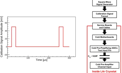
This section describes the in-situ calibration of the MicroBooNE LArTPC cold electronics using an externally generated signal injected into the pre-amplifier channel inputs. Calibrating the cold electronics response allows for a direct comparison between the ideal and real electronics responses. This in-situ calibration can also be used to improve the accuracy of simulated data and signal processing algorithms. It is also of interest to determine the uniformity of the electronics response. Finally, repeating the calibration measurement periodically is required in order to evaluate the stability of the electronics response over time.
2.1 MicroBooNE TPC cold electronics calibration system
The MicroBooNE cold electronics calibration system uses a signal generator located outside the cryostat to provide a calibration signal to each individual cold electronics channel input, as
sum-marized in figure 2. The signal generator produces a square wave signal that is fanned out and
each pre-amplifier input individually through a∼183 fF capacitor. The ASICs must be configured
to connect the test signal input pin to the calibration capacitors; during normal detector operation they are disconnected. The capacitively coupled square wave calibration signal injects a known
amount of charge into the pre-amplifier input on a timescale of ∼10 ns, which is much shorter
than the nominal pre-amplifier peaking time of 2 µs. Consequently the resulting signal waveform approximates the impulse response of the cold pre-amplifiers. An example of a digitized calibration
signal waveform is shown in figure3.
s] µ Time [
0 100 200 300
Calibation Signal Amplitude [mV] −20
0 20 40 60
Square-Wave Signal Generator
Calibration Signal Fanout
Service Boards and Cables
Cold Motherboards
Cold Pre-Pmplifying ASICs Test Input Pin
Inside LAr Cryostat
Cin ~183fF
[image:10.595.87.511.204.456.2]Cold Pre-Amplifier Channel Input
Figure 2: Schematic overview of the MicroBooNE cold electronics calibration signal system. The
plot shows a∼50 mV square wave voltage signal, generated outside the LAr cryostat and propagated
to the cold electronics channel inputs via the calibration injection system, shown schematically in the graphic. Copies of the square wave voltage signal are generated with a fanout module and transmitted into the cryostat through dedicated service boards and cables. The signal is routed to
every cold electronics ASIC test input pin and coupled to each pre-amplifier input through a∼183
fF capacitor.
A number of channels of the cold electronics are considered non-functional and cannot be
calibrated, with the specific causes discussed in Ref. [14]. Roughly 220 channels (out of 8256) of
the cold electronics are located on ASICs that cannot be configured due to a hardware failure of the configuration chain from a service board through the cold cable to the cold electronics inside the cryostat. These channels are still used to measure ionization charge but can only use the default 4.7 mV/fC gain and 1 µs peaking time settings. Calibration signals can not be injected into these channels as the ASICs must be specifically configured to enable the test input pin. An additional
∼860 channels are not functioning correctly and similarly can not be calibrated. These channels
Figure 3: Example of a digitized waveform from an injected calibration signal on a single collection
plane channel, including a fit to the electronics response function (overlaid in red). The fitted peaking
timetpis 2.15±0.01 µs and the amplitude A0is 599±3 ADCs.
approximately stable in number over time as discussed in Ref. [14].
2.2 Electronics response parameterization
The impulse response of the TPC cold electronics is well described by a fifth-order semi-Gaussian
anti-aliasing filter. The representation of this function in the time domain is shown in figure3and
is parameterized by
R(t,A0,tp)=A1E1−A2E2(cosλ1+cosλ1cosλ2+sinλ1sinλ2)
+A3E3(cosλ3+cosλ3cosλ4+sinλ3sinλ4)
+A4E2(sinλ1−cosλ2sinλ1+cosλ1sinλ2)
−A5E3(sinλ3−cosλ4sinλ3+cosλ3sinλ4).
(2.1)
The parameters in Eq.2.1are obtained from a detailed simulation of the filter design and given
by:
A1 =4.31054A0, A2 =2.6202A0,
A3 =0.464924A0, A4 =0.762456A0, A5=0.327684A0,
E1 =e −2.94809t
t p , E
2 =e −2.82833t
t p , E
3= e −2.40318t
t p ,
λ1 =1.19361 t
tp
, λ2 =2.38722 t
tp ,
λ3 =2.5928 t
tp
, λ4 =5.18561 t
tp ,
(2.2)
wheretis time in µs, tp is the peaking time constant in µs, and A0 is the amplitude parameter in
Electronics response calibration data are recorded while the detector is in its normal operational state. The cold electronic pre-amplifier ASICs are configured to use their default settings with the exception that the calibration signal input is enabled for every electronics channel in the detector. Calibration signal pulse shapes are identified in digitized waveform data and the leading edge fitted
using the response function described in Eq.2.1. Calibration signal amplitude and peaking time
parameters for each channel are obtained from these fits. The results of these fits are used to parameterize the electronics response for each channel.
Electronics channel gain can be derived from the fitted calibration pulse amplitude given the known amplitude of the injected signals. These gain measurements need to be corrected to account for attenuation introduced by the calibration signal injection system. The most important correction to electronics response gain measurements is due to the calibration signal fanout modules. A pair of modules receives the analog calibration signal from the function generator and propagates copies to each set of motherboards sharing common service cables. The calibration signal input for one of these modules is output from the other, and this daisy-chained configuration attenuates the second calibration signal copy. This can be observed directly by comparing calibration signal average pulse height measurements for sets of channels connected to each module, as in the top row of
figure4. A correction is applied to the gain measurements for channels receiving the calibration
module attenuated signal to remove this effect. A similar correction removes variations in gain measurements due to service cable attenuation. These corrections are constant over time, although there are two sets of service cable attenuation corrections corresponding to the periods before and after a service board hardware upgrade was performed in summer 2016. Calibration signal injection
is observed to induce electronic crosstalk into adjacent channels with a bipolar signal size∼1% of
the calibration pulse height, which is small enough to not require any correction.
The gain measurements after applying the previously defined calibration module fanout and
service cable corrections are shown in the bottom row of figure4. There is a systematic
discrep-ancy in measured gain between channels configured with the collection baseline setting and those
configured with the induction baseline setting, as shown in figure5, that is an intrinsic feature of the
cold pre-amplifiers. Channels configured to use the induction baseline setting have an average
mea-sured gain of 194.3±2.8 [e−/ADC] while the average collection-mode channel gain is 187.6±1.7
[e−/ADC]. This discrepancy contributes to some of the residual variations in the induction wire
corrected gain measurements as a subset of induction plane channels are misconfigured to use the
collection 200 mV baseline setting. The variation in the∼183 fF test signal injection capacitors
is∼0.5%, which contributes to the observed variation in these gain measurements. Additionally,
these gain measurements are also expected to have a systematic bias due to the overall average attenuation introduced by the calibration injection system. Calibration methods such as measuring energy deposition from minimimum ionizing particles are required to measure the absolute gain given the inability to measure this overall attenuation factor in-situ.
The electronics response peaking time parameter is obtained from fits to calibration signals for each cold pre-amplifier channel individually. Peaking time parameters are not measured for
misconfigured or non-functioning channels. The mean peaking time is 2.18±0.08 µs, which is
∼10% higher than the nominal value of 2 µs, due to the additional input capacitance from the TPC
wires. The overall variation in fitted pre-amplifier peaking time is∼3%, which is significantly less
Induction Plane Wire Number
0 500 1000 1500 2000
Gain [e- / ADC Counts]
180 185 190 195 200 205 210
U Plane Channels
V Plane Channels
MicroBooNE
(a) Uncorrected gain for induction plane channels.
Collection Plane Wire Number
0 500 1000 1500 2000 2500 3000
Gain [e- / ADC Counts]
180 185 190 195 200 205 210
Y Plane Channels
MicroBooNE
(b) Uncorrected gain for collection plane channels.
Induction Plane Wire Number
0 500 1000 1500 2000
Corrected Gain (e- / ADC Counts) 180 185 190 195 200 205 210
U Plane Channels
V Plane Channels
MicroBooNE
(c) Corrected gain for induction plane channels.
Collection Plane Wire Number
0 500 1000 1500 2000 2500 3000
Corrected Gain (e- / ADC Counts) 180 185 190 195 200 205 210
Y Plane Channels
MicroBooNE
[image:13.595.301.493.94.208.2](d) Corrected gain for collection plane channels.
Figure 4: Uncorrected gain measurement for every TPC induction (a) and collection (b) plane
channel. Also shown is the induction (c) and collection (d) channel gain measurement after correcting for both calibration module attenuation and service cable dependence. The first few hundred U Plane channels cannot be calibrated due to the inability to configure the cold electronic ASICs, and are not plotted here. A subset of induction plane channels are misconfigured to use the collection 200 mV baseline setting, which contributes to some of the residual variations in the induction wire corrected gain measurements.
by the implementation of the calibration system but is a feature of the pre-amplfiier ASICs. Figure
6 suggests that the source of this variation is a disagreement in the shape of the ideal and real
electronics response. In particular, the real electronics response has much longer tails than does the ideal response, which is a known feature in this version of the cold electronic ASICs and has been
addressed in a subsequent version of the electronics [22].
The observation of non-ideal components in the calibration signal waveforms suggests that parameterizing the response in terms of the idealized response may introduce bias in charge mea-surements when comparing data to simulation. As an alternative, it is possible to measure the average impulse electronics response shape from calibration signals and use this in place of the
Corrected Gain [e- / ADC Counts]
180 185 190 195 200 205 210
Number of Channels
0 100 200 300 400 500 600 700 800
900 Collection Channels
Induction Channels
MicroBooNE
Figure 5: Measured TPC electronics pre-amplifier gain after applying calibration fanout module
and service cable corrections. A systematic discrepancy is observed between collection channels and induction channels, an understood feature of the pre-amplifier. The average measured gain of
the induction channels is 194.3±2.8 [e−/ADC] while the average measured gain of the collection
channels is 187.6±1.7 [e−/ADC].
s]
µ
Time [
0 20 40 60 80
Arb. Units
0 0.5 1
Example Overshoot Response
Example Undershoot Response
Ideal Response
MicroBooNE
Figure 6: Example calibration signal waveforms, averaged over many signal pulses, with clearly
visible extended tails. These extended tails are not well described by the ideal electronics response, which is also shown for comparison (black). This is a known feature in this version of the cold
electronic ASICs and has been addressed in a subsequent version of the electronics [22]. These
Calibration Run Date
2016-07-01 2016-12-31 2017-07-02
Average Gain [e-/ADC counts]
185 190 195 200Collection Plane
Induction Plane
MicroBooNE
Figure 7: Gain measurements of the TPC cold electronics channels taken over time, with red and
blue colored bands representing the RMS variation of the corrected channel gain in the induction and collection planes, respectively. The average discrepancy in channel gain measurements between calibration data runs is less than 0.2% and is significantly smaller than the variation in channel gain within the induction and collection wire planes.
2.3 Stability of electronics response
In order to apply electronics response measurements in signal processing algorithms, it is necessary to demonstrate that the response is stable over time. If the response changes significantly over time, there is the potential to bias ionization charge measurements by using response parameters that are not appropriate for a given time period. The stability of the electronics response is evaluated by comparing the measured electronics response parameters from calibration runs spaced several months apart. It is observed that the measured cold pre-amplifier gain is very stable over this
timescale, as shown in figure7, with an average deviation less than 0.2% across all measurements.
2.4 Validation of electronics response correction
In this section we demonstrate how the measured average response waveforms can correct the observed non-uniform and non-ideal electronics response. This correction is achieved through a 1D
deconvolution based on discrete-space Fourier transformation techniques described in section1.1.
The correction can be defined in the frequency domain as:
Micorr(ω)= Mi(ω) ·
Rideal(ω) Ri(ω)
, (2.3)
whereωis in units of angular frequency,Rideal(ω)is the Fourier transform of the ideal electronics
response function and Ri(ω) is derived from the measured average electronics response for the
ith channel. Since the Rideal and Ri are generally similar, the change in the electronics noise
s] µ Fitted Peaking Time [
2 2.05 2.1 2.15 2.2 2.25 2.3 2.35 2.4
Number of Channels
0 500 1000 1500 2000 2500 3000 3500 4000
Before Correction After Correction
MicroBooNE
Figure 8: Peaking time measurement for the channels of the TPC cold electronics before (blue)
and after (red) the electronics response correction. The overall variation in the measured peaking
time after applying the electronics response correction is ∼0.8% compared to∼3.5% before the
correction.
time (i.e. independent of any other channels). Therefore, it can be applied before the general 2D
deconvolution [12] dealing with the long range effect of the field response across multiple wires.
The electronics response correction defined in Eq.2.3is applied to injected calibration signals
in order to evaluate the impact on the shape of the impulse response. Injected calibration signals with and without the electronics response correction applied are fitted with the ideal electronics
response function. The distributions of the measured peaking times are summarized in figure8. The
calibration signal shapes are significantly more uniform after the electronics response correction is
applied, with∼0.8% variation in the measured peaking time parameter after the correction compared
to the original∼3% variation.
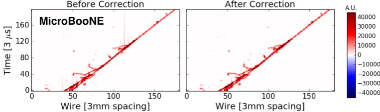
This correction is also evaluated by applying it to signals produced by a cosmic muon track
recorded during normal detector operations as shown in figure9. This and following event displays
MicroBooNE
(a) Event displays before and after electronic response correction.
3200 3400 3600 3800 4000
s] µ Time [
0 100 200 300
Sample Value [ADC counts]
Before Correction
After Correction
MicroBooNE
[image:17.595.89.471.93.206.2](b) Waveform before and after electronic response correction.
Figure 9: Example event displays showing the Y plane view from Event 0, Run 3455 (a) before
and after the application of the electronic response correction defined in Eq.2.3in units of average
baseline subtracted ADC scaled by 250 per 3 µs. The long tails (faint vertical stripes going upward from the track) seen on certain collection plane channels following large charge signals are largely removed by the correction. The effect of the correction on an individual digitized waveform (b) also clearly shows this tail removal.
3 Validation of field response function simulation with data
As discussed in section1, the characteristics of TPC signals are dictated by the initial ionization
charge cloud formation within the detector bulk, the signals created on the TPC wires due to the drift of the ionization electrons near the wires (field response), and the shaping of the signals via the front-end electronics (electronics response). In the previous section, the calibration of the electronics response was discussed. This section now focuses on the nature of the wire field response, which must be probed with ionization signals as opposed to signals from the electronics
calibration system described in section2.
In order to validate the simulation of the wire field response and electronics response [12], we
Z
Y
Figure 10: Illustration of the subregions of the TPC active volume that are used to study the
different wire field responses from data, looking at a view of the anode plane (y − z plane).
Depicted are the “shorted-U” and “shorted-Y” regions in red and blue, respectively. Also shown is the subregion of the “normal” region used to study the nominal field response shapes (area inside dashed magenta box). The TPC dimensions in the illustration are roughly 2.3 meters in the
ydirection and 10.4 meters in thezdirection.
utilizing a data-driven technique to produce comparisons of simulation and data at the waveform
level. In section 3.1, the data-driven method used to make this comparison is described. In
particular, comparisons of the full response, which is the convolution of the wire field response and electronics response, are made. Despite making comparisons of the full response, this method primarily demonstrates how well we simulate the wire field response, as the electronics response is
first calibrated in data using the cold electronics calibration system (see section2). The consistency
of the wire field response between data and simulation is also an indirect validation of the signal processing chain that is used to “remove” the field and electronics response from the waveform, which is done in order to extract the amount of charge seen on the TPC wires. Correctly modeling the wire field response and electronics response allows for an unbiased estimation of ionization charge on the TPC wires in data.
There is an additional complication due to there being multiple regions within the TPC ex-hibiting non-standard wire field responses. This is due to the shorting of channels across wire
planes in particular regions of the TPC, as described in Ref. [14]. The nature of the shorting of
channels between the different wire planes has not been observed to change since the beginning of data-taking at MicroBooNE. The different bias voltages seen on channels in these regions lead to different induced current distributions as ionization electrons move past the wires. In addition to the “normal” region, where there are no shorted channels, there is a “shorted-U” region where multiple U plane channels are shorted to one or more V plane channels, and a “shorted-Y” region where multiple Y plane channels are shorted to one or more V plane channels. The wire field responses are extracted separately in these different regions and the response is assumed to be uniform within
each of these regions. These subregions are illustrated in figure10. Similar to the normal region, the
field response simulation in the shorted-channel regions is done using Garfield with identical wire
geometry as described in Ref. [12], in which the signal formation mechanism has been elaborated
After discussing the data-driven method used to extract the full response from data in section3.1,
comparisons of the full responses in data and simulation are made for the normal region in section3.2
and for the shorted-U and shorted-Y regions in section3.3. The detailed Garfield simulation steps
are also discussed in section3.3, focusing on the differences between the simulation in the normal
and shorted-channel regions. Finally, in section3.4the special treatment of the shorted-Y region in
the signal processing chain is discussed.
3.1 Response extraction methodology
In order to compare the full response in data to that predicted by simulation, a track-based data-driven method is used to extract the full response from off-beam cosmic ray data (data recorded when it is known that no beam-related neutrinos are passing through the MicroBooNE detector).
This is done by i) determining the value oft0, wheret0 refers to the time at which the cosmic ray
enters the TPC volume, ii) ensuring that a substantial amount of light is seen by the MicroBooNE
photomuliplier tubes (PMTs) [23] at the time corresponding to the value oft0found, iii) correcting
the drift coordinate, x, of the cosmic ray track in the TPC to the location the cosmic ray actually
traversed through the TPC, and iv) coherently adding the waveforms associated with thet0-tagged
track to recover a clean representation of the signal shape from the waveform while suppressing the noise on the waveform. The MicroBooNE PMT system (32 PMTs located behind the anode plane)
is used both for thist0-tagging of cosmic tracks as well as for triggering on light associated with
beam events within the detector, which is used to enhance the purity of neutrino interaction signal
events in the recorded data stream. The motivation for usingt0-tagged tracks for the data/simulation
comparison comes from the desire to minimize the effects of diffusion in the full response estimation. This can be done by utilizing only parts of tracks very close to the anode plane where effects of diffusion are minimal. One must know the drift coordinate of the tracks in order to ensure this
condition, necessitating the use oft0-tagged tracks.
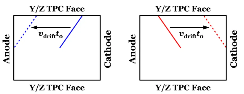
Thet0-tagging method used in these studies is visualized in figure11. First, a sample of data
events (on order of 10k) are collected from the MicroBooNE detector using off-beam triggers (data collected at periodic intervals while the beam is not active), providing a large set of cosmic rays (more than 100k) for study without contamination from neutrino interaction events. The track associated with each cosmic ray is then reconstructed in three dimensions (3D) using the Pandora
multi-algorithm pattern recognition [24] employed on TPC data. The cosmic ray is assumed to be
through-going (passing through two faces of the TPC). This is a good assumption as most cosmic rays have high enough momentum to pass through the TPC completely without stopping. Next, the
track is required to either enter or exit a TPC face iny(top or bottom of TPC) orz(front or back of
TPC, with respect to direction of the beam), but not both. If this condition is met, and the cosmic ray is through-going (as assumed), the cosmic ray must either enter or exit the anode or cathode.
Depending on the angle that the reconstructed track makes in the y− x plane, the cosmic ray is
then determined to be either “anode-piercing” or “cathode-piercing” (see figure11), and the value
oft0is assigned based upon the time tick associated with the signal on the waveform at the part of
the track closest to either the anode or cathode, respectively. A “flash” of light seen in several of
MicroBooNE’s 32 eight-inch PMTs is required to be found at the same time as the determinedt0
value in order to increase the purity of thet0-tagging technique. Finally, the drift coordinate of the
A
n
o
d
e
C
a
th
o
d
e
Y/Z TPC Face
Y/Z TPC Face
v
driftt
0(a) Examplet0-tagging of anode-piercing track.
A
n
o
d
e
C
a
th
o
d
e
Y/Z TPC Face
Y/Z TPC Face
v
driftt
0 [image:20.595.94.506.87.247.2](b) Examplet0-tagging of cathode-piercing track.
Figure 11: Illustration of thet0-tagging method used in the studies presented in this work. The
drift coordinate (x) of cosmic ray tracks are corrected using the assumption that the cosmic ray
is through-going, requiring the track to pass through only one TPC face in y or z, and using the
angle of the track in the y− x plane (or z− x plane) to determine if the track is anode-piercing
(a) or cathode-piercing (b). The known ionization electron drift velocity,vdrift, then allows for the
correction of the drift coordinate of the cosmic ray track. The track before and after the correction
is shown by the solid and dashed lines, respectively. Before the correction (when thet0of the track
is assumed to be the trigger time), the track falsely appears to stop in the middle of the TPC.
liquid argon at an electric field of 273 V/cm,vdrift =0.1114 cm/µs [25]. Validations using Monte
Carlo simulation and data-driven validations utilizing an external small cosmic ray tagger [26]
have shown thist0-tagging method to reconstruct the trackt0correctly at least 98% of the time for
anode-piercing tracks and at least 97% of the time for cathode-piercing tracks.
With the drift coordinate of the cosmic ray track corrected, one can proceed to use the subset of anode-piercing tracks (roughly one per recorded off-beam event) to estimate the full response via the method described above. Only waveforms associated with the portion of the track between 2 cm and 10 cm away from the anode plane are used in order to minimize the influence of diffusion, which is why anode-piercing tracks are used instead of cathode-piercing tracks. Waveform signals are lined up in time across many different wires (and tracks from different events) and are added together. This can be done as cosmic muons are well-approximated by straight lines, so the signal can be assumed to be coherent across a short distance of the cosmic muon track. For unipolar signals, such as those observed by the collection plane wires, the positive signal peak is the feature lined up in time; in contrast, for the bipolar signals of the induction plane wires, the negative dip of the signal is instead lined up in time. The coherent nature of the signal across waveforms associated with different wires leads to the signal response being preserved when the waveforms are added together. Conversely, noise on the waveform averages out as it is incoherent across different wires. The result is a data-driven estimate of the full response for each plane in each of the regions.
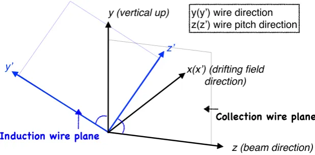
The coordinate system used for these studies is described in figure12a. For each wire plane,
y’
z’
z (beam direction) y (vertical up)
x(x’) (drifting field direction)
Collection wire plane
Induction wire plane
y(y’) wire direction z(z’) wire pitch direction
(a) Coordinates for collection and induction planes. They0(z0) axis is rotated by 60◦
around xaxis fromy(z) axis.
x(drifting field direction) y(wire direction)
z(wire pitch direction)
theta_xz theta_y
𝜽
𝒚
𝜽
𝒙𝒛
(b) Definition of two angles,θxz andθy, which define the direction of a track in the
[image:21.595.146.456.99.251.2]TPC.
Figure 12: Geometric coordinates (a) and angles for description of track topology (b).
along the wire orientation, and thez-axis is along the wire pitch direction. Different coordinates
are used for each wire plane, as the wire directions of the different planes are at an angle to one
another; the induction planes use the “primed” coordinate system as shown in figure12a. The
nominal (default) detector coordinate system is identical to the Y plane’s coordinate system for
which the y-axis is vertical in the upwards direction (toward the sky) and thez-axis is along the
direction of the neutrino beam. The origin of the coordinate system is located at the center of the U plane’s upstream edge (the edge closest to the source of the neutrino beam). Based on the predefined coordinate for each wire plane, two angles define the direction of the track. As shown
in figure12b, θy is the angle between the track and the y-axis, andθxz is the angle between the
projection onto thex−zplane and thez-axis.
In estimating the full response, only tracks with 5◦ < θ
the impulse response of the drifting ionization electrons is well approximated, though cross-checks of the signal simulation against data are also performed at higher track angles. By repeating the measurement using a Monte Carlo simulation of cosmic ray tracks, it is determined that there is a Gaussian smearing of approximately 1 µs introduced by the method itself. The origin of this smearing is from the alignment of signals in time across many different waveforms, which introduces a slight broadening to the resulting average response. When making comparisons of the full response between data and simulation, this Gaussian smearing is applied to the simulation.
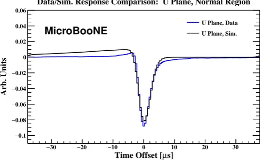
3.2 Response in normal region
By applying the methodology discussed earlier in this section, the full response in the normal region is extracted from data and compared to the convolution of the wire field response simulated by Garfield with a parametrization of the electronics response function for a given peaking time (2.2 µs in this case to match the effective peaking time seen in data). The comparison of the full
response for data to that for the simulation in the normal region is illustrated in figure13. The
absolute normalization of the full responses is arbitrary and only fixed relative to the integral of the Y plane response, which is set to unity.
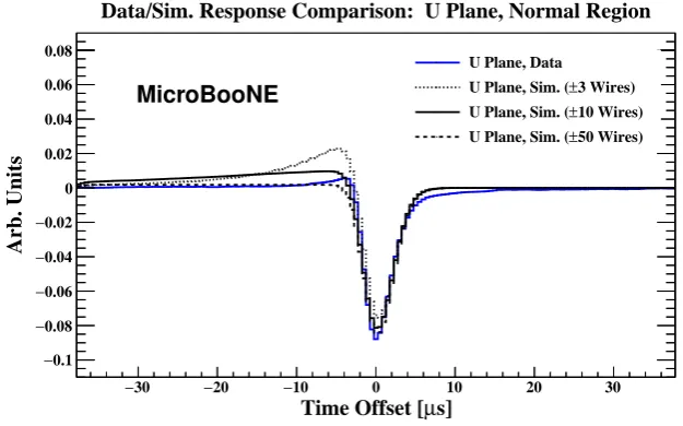
In general there is quite good agreement between data and simulation, though there are a few differences worth pointing out. First of all, the U plane “front porch” or the slow-rising feature of the waveform in front of (at lower values of time) the primary “dip” exhibits some disagreement between data and simulation. This feature is due to the absence of a shield plane in front of the U plane in MicroBooNE, allowing charge further away from the anode plane to produce a signal on the unshielded U plane wires during drift (if there were a shield plane in front of the U plane, the U plane and V plane wire field responses would look very similar). The disagreement between data and simulation can be attributed to the finite number of wires that are adjacent to the wire closest to the drifting ionization electrons included in the Garfield simulation of the wire field response (10 wires on either side of the primary wire in the results shown). The impact of changing the number of adjacent wires in the Garfield simulation on the U plane full response is shown in
figure14. Increasing the number of adjacent wires would likely reduce the front porch feature even
more in the simulation, at the cost of increased computation time. However, the impact on charge reconstruction from this effect is expected to be small.
In addition to differences in the “front porch” feature of the U plane, in figure13we can see
a small discrepancy in the width of the signals between data and simulation. This difference in signal width is most noticeable on the Y plane but can also be seen on the U and V planes. The difference can potentially be explained by 3D effects that are not included in the Garfield simulation, which assumes that the wires of the different wire planes are parallel to one another and neglects the complicated drift of the ionization electrons through the wire planes in three dimensions. A potential improvement in the future is to use a full 3D simulation of the wire field response that is currently computationally expensive and too imprecise to utilize at present. The development of a sufficiently precise 3D simulation of the wire field response is in progress.
As described in Ref. [12], charge induction on wires adjacent to the wire that is closest to
drifting ionization charge can lead to large contributions to the signals observed on TPC wires. This effect is more noticeable when an ionization track is at higher angle with respect to the anode plane
s]
µ
Time Offset [ 30
− −20 −10 0 10 20 30
Arb. Units
0.1 − 0.08 −
0.06 −
0.04 −
0.02 −
0 0.02 0.04 0.06
U Plane, Data
U Plane, Sim. Data/Sim. Response Comparison: U Plane, Normal Region
s]
µ
Time Offset [ 30
− −20 −10 0 10 20 30
Arb. Units
0.08 −
0.06 −
0.04 −
0.02 −
0 0.02 0.04 0.06 0.08
V Plane, Data
V Plane, Sim. Data/Sim. Response Comparison: V Plane, Normal Region
s]
µ
Time Offset [ 30
− −20 −10 0 10 20 30
Arb. Units
0.02 −
0 0.02 0.04 0.06 0.08 0.1 0.12 0.14
Y Plane, Data
Y Plane, Sim. Data/Sim. Response Comparison: Y Plane, Normal Region
[image:23.595.149.421.91.265.2]MicroBooNE
Figure 13: Data/simulation comparison of the full response for the different wire planes in the
s] µ Time Offset [
30
− −20 −10 0 10 20 30
Arb. Units
0.1
−
0.08
−
0.06
−
0.04
−
0.02
−
0 0.02 0.04 0.06 0.08
U Plane, Data 3 Wires)
±
U Plane, Sim. (
10 Wires)
±
U Plane, Sim. (
50 Wires)
±
U Plane, Sim. (
Data/Sim. Response Comparison: U Plane, Normal Region
[image:24.595.124.437.89.284.2]MicroBooNE
Figure 14: Comparison of U plane full response (electronics response convolved with wire field
response) simulation to data, using a variable number of wires adjacent to the wire closest to the
ionization electrons in the Garfield simulation: ±3,±10, and±50. This comparison is made in the
region of the TPC unimpaired by shorted channels (normal region). The “front porch" of the U plane wire field response becomes less pronounced when the simulation utilizes a greater number of wires, converging to what is seen in data. A small positive peak before the “dip” of the U plane response is observed in data and is not reproduced in the simulation when utilizing any number of wires. This discrepancy is likely due to signal fluctuations present in data that are not included in the simulation.
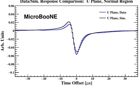
seen in data, a similar comparison to that illustrated in figure13is shown in figure15using tracks
with 40◦ < θ
xz < 50◦. The comparison shown in figure15indicates that the simulation performs
quite well in reproducing the effect of charge induced on wires neighboring the wire closest to drifting ionization. There are minor discrepancies that would likely be reduced with an improved simulation of wire field response, as discussed above. This includes a disagreement in the “front porch” region of the U plane wire field response and an additional discrepancy between data and simulation for the Y plane wire field response, for which the simulation predicts a small dip in the
later part (att≈5 µs) of the waveform that is not observed in data.
3.3 Response in shorted-wire regions
The comparison of the full response in data and simulation made in section3.2is repeated for the
the shorted-U and shorted-Y regions. In these regions, while the electronics response remains the
same as in the normal region, the wire field response differs dramatically, as shown in figure16.
This is due to the different drift paths and velocities that ionization electrons experience as they drift through the anode plane wires, as a result of the different bias voltages on the shorted channels. Given the lack of information available regarding the nature of the short, data must be utilized in order to best model the true detector condition.
s]
µ
Time Offset [ 30
− −20 −10 0 10 20 30
Arb. Units
0.1 − 0.08 −
0.06 −
0.04 −
0.02 −
0 0.02 0.04 0.06
U Plane, Data
U Plane, Sim. Data/Sim. Response Comparison: U Plane, Normal Region
s]
µ
Time Offset [ 30
− −20 −10 0 10 20 30
Arb. Units
0.08 −
0.06 −
0.04 −
0.02 −
0 0.02 0.04 0.06 0.08
V Plane, Data
V Plane, Sim. Data/Sim. Response Comparison: V Plane, Normal Region
s]
µ
Time Offset [ 30
− −20 −10 0 10 20 30
Arb. Units
0.02 −
0 0.02 0.04 0.06 0.08 0.1 0.12 0.14
Y Plane, Data
Y Plane, Sim. Data/Sim. Response Comparison: Y Plane, Normal Region
[image:25.595.148.422.103.280.2]MicroBooNE
Figure 15: Comparison of the signal simulation for the different wire planes to data using tracks
with 40◦ < θ
xz < 50◦, looking at the region of the TPC unimpaired by shorted channels (normal
[ ]
[
]
(a) Shorted-U region.
Wire Pitch Distance[ ]
Drift Distance
[
] S Y
[image:26.595.106.495.79.280.2](b) Shorted-Y region.
Figure 16: The trajectories of ionization electron drift as a demonstration of the simulation of the
electric field near the wire planes using Garfield. The ionization drift lines associated with the shorted-U region (a) and shorted-Y region (b) are shown, with a comparison made to the normal region in both cases. A couple of features are worth noting. In the case of the shorted-U region, a fraction of the charge that would be collected by the Y plane is instead collected by the unresponsive U plane wires, leading to a decreased transparency of the ionization electrons as seen by the V plane and Y plane wires. In the case of the shorted-Y region, ionization electrons that are normally collected by the Y plane are instead collected on the V plane wires, leading to unipolar (as opposed to bipolar) signals on the V plane wires in this region of the detector.
the short is that one or more wires in the V plane physically touch a group of wires in the U plane or Y plane; however, a visual inspection of the wire planes (prior to filling the cryostat with argon) via the use of a camera inserted into the cryostat yielded no evidence of wires physically touching each
other [27]. In principle, the bias voltage on the wires shorted by this cross-plane contact should
be reduced to the ground level because of the contact with the V plane, which is held at detector ground. However, the fact that the sensitive wire is connected to a pair of diodes with 1.8 V bias for the pre-amplifier and ground, respectively, provides a hint that the actual bias on the wires may be different from ground. An imperfect short may cause residual voltage on the shorted channel significantly different from ground, with the supply bias set at -110 V and +230 V for the U plane and Y plane, respectively. Thus, the bias voltages on the shorted channels are set to values different from ground in the Garfield simulation in such a way as to reproduce the field response function shape as seen in data. For the shorted-U region, it was found that setting the bias voltage to -45 V leads to good agreement between data and simulation. A bias voltage of +20 V on the Y plane wires in the shorted-Y region is necessary to best match the simulation to data.
The data/simulation comparison for the shorted-U region is made in figure17, utilizing tracks
with 5◦ < θ
xz <15◦. As for the case of the normal region, the absolute normalization is arbitrary
s]
µ
Time Offset [ 30
− −20 −10 0 10 20 30
Arb. Units
0.08 −
0.06 −
0.04 −
0.02 −
0 0.02 0.04 0.06 0.08
V Plane, Data
V Plane, Sim. Data/Sim. Response Comparison: V Plane, Shorted U Region
s]
µ
Time Offset [ 30
− −20 −10 0 10 20 30
Arb. Units
0.02 −
0 0.02 0.04 0.06 0.08 0.1 0.12 0.14
Y Plane, Data
Y Plane, Sim. Data/Sim. Response Comparison: Y Plane, Shorted U Region
[image:27.595.149.421.90.262.2]MicroBooNE
Figure 17: Data/simulation comparison of the full response for the different wire planes in the
shorted-U region. Simulation is shown in black, while the colored curves represent the full response
extracted from data using tracks with 5◦ < θ
xz < 15◦. The simulation predicts a slightly broader
response than that observed in data, potentially due to the simulation neglecting ionization electron
drift in three dimensions (see section3.2).
features observed in data are reproduced with the modified Garfield simulation. As mentioned above, the transparency to ionization drift in this region of the TPC is reduced due to some of the ionization electrons being collected by the U plane wires, leaving less charge to induce a signal on the V plane and to be collected by the Y plane. The U plane response is not shown in this region as the U plane wires are unresponsive due to the short between the U and V planes.
The same comparison is made for the shorted-Y region in figure 18, again using tracks with
5◦ < θ
xz < 15◦. As expected, the U plane response is largely the same as in the normal region
s]
µ
Time Offset [ 30
− −20 −10 0 10 20 30
Arb. Units
0.1 − 0.08 −
0.06 −
0.04 −
0.02 −
0 0.02 0.04 0.06
U Plane, Data
U Plane, Sim. Data/Sim. Response Comparison: U Plane, Shorted Y Region
s]
µ
Time Offset [ 30
− −20 −10 0 10 20 30
Arb. Units
0.04 −
0.02 −
0 0.02 0.04 0.06 0.08 0.1 0.12
V Plane, Data
V Plane, Sim. Data/Sim. Response Comparison: V Plane, Shorted Y Region
[image:28.595.148.421.90.263.2]MicroBooNE
Figure 18: Data/simulation comparison of the full response for the different wire planes in the
shorted-Y region. Simulation is shown in black, while the colored curves represent the full response
extracted from data using tracks with 5◦ < θ
xz < 15◦. As in the normal region, a small discrepancy
is observed between data and simulation in the “front porch” of the U plane response that can be reduced by adding more wires into the wire field response simulation.
loss of transparency for ionization electrons drifting through the anode wire planes. The modified Garfield simulation can reproduce the features seen in data in this region, in particular the shape of the unipolar V plane response. The disagreement between data and simulation in the “front porch”
of the U plane response is similar to that observed in the normal region, discussed in section3.2.
The Y plane response is not shown in figure18because the Y plane wires are unresponsive in this
region.
3.4 Signal processing for shorted-wire regions
![Figure 1: Illustration of signal formation in the MicroBooNE three-plane LArTPC, depicting theV plane (second induction plane) and Y plane (collection plane) TPC wire signals on the right ofthe image [9].](https://thumb-us.123doks.com/thumbv2/123dok_us/9315969.433328/6.595.113.465.123.380/figure-illustration-formation-microboone-lartpc-depicting-induction-collection.webp)