Motorola reserves the right to make changes without further notice to any products herein to improve reliability, function or design. Motorola does not assume any liability arising out of the application or use of any product or circuit described herein; neither does it convey any license under its patent rights nor the rights of others. Motorola products are not designed, intended, or authorized for use as components in systems intended for surgical implant into the body, or other applications intended to support or sustain life, or for any other application in which the failure of the Motorola product could create a situation where personal injury or death may occur. Should Buyer purchase or use Motorola products for any such unintended or unauthorized application, Buyer shall indemnify and hold Motorola and its officers, employees, subsidiaries, affiliates, and distributors harmless against all claims, costs, damages, and expenses, and reasonable attorney fees arising out of, directly or indirectly, any claim of personal injury or death associated with such unintended or unauthorized use, even if such claim alleges that Motorola was negligent regarding the design or manufacture of the part.
ATD_10B8C
Block User Guide
V02.10
Original Release Date: 27 OCT 2000 Revised: 21 Feb. 2003
Revision History
Table 0-1 Revision History Version
Number
Revision Date
Effective
Date Author Description of Changes
00.00 27-10-2000 - Initial SRS2 release.
01.00 06-06-2001 - Updated the description of ATDDIEN and PORTAD1 register.
01.10 16-06-2001 - Made SRS2 Compliant
V02.00 20 June 2001
20 June
2001 Reworked whole document to make it more user friendly
V02.01 26 July 2001 - Added document names
Variable definitions and names have been hidden
V02.02 5 Sept 2001 5 Sept 2001 Corrected sampling phase description, other minor corrections V02.03 8 Nov 2001 8 Nov 2001 Corrected AWAI bit description
V02.04 16 Jan 2002 16 Jan 2002 Syntax corrections
V02.05 8 Mar 2002 8 Mar 2002 Removed document number from all pages except cover sheet V02.06 11 Apr 2002 11 Apr 2002 Documented special channel conversion in ATDTEST1 register V02.07 22 Apr 2002 22 Apr 2002 Corrected Table "Available Result Data Formats"
V02.08 16 Aug 2002 16 Aug 2002 FIFOR flag: corrected clearing mechanism B)
V02.09 23 Aug 2002 23 Aug 2002
Detailed AWAI Bit description.
Functional Description: Detailed and corrected Low power modes
Table "Available Result Data Formats": Re-corrected
Table of Contents
Section 1 Introduction
1.1 Overview. . . .9
1.2 Features . . . .9
1.3 Modes of Operation . . . .9
1.3.1 Conversion modes . . . .9
1.3.2 MCU Operating Modes . . . .9
1.4 Block Diagram . . . .10
Section 2 Signal Description
2.1 Overview. . . .112.2 Detailed Signal Descriptions. . . .11
2.2.1 AN7 / ETRIG / PAD7 . . . .11
2.2.2 AN6 / PAD6 . . . .11
2.2.3 AN5 / PAD5 . . . .11
2.2.4 AN4 / PAD4 . . . .11
2.2.5 AN3 / PAD3 . . . .11
2.2.6 AN2 / PAD2 . . . .11
2.2.7 AN1 / PAD1 . . . .11
2.2.8 AN0 / PAD0 . . . .11
2.2.9 VRH, VRL. . . .12
2.2.10 VDDA, VSSA . . . .12
Section 3 Memory Map and Register Definition
3.1 Overview. . . .133.2 Module Memory Map . . . .13
3.3 Register Descriptions . . . .14
3.3.1 Reserved Register (ATDCTL0) . . . .14
3.3.2 Reserved Register (ATDCTL1) . . . .14
3.3.3 ATD Control Register 2 (ATDCTL2). . . .14
3.3.4 ATD Control Register 3 (ATDCTL3). . . .16
3.3.5 ATD Control Register 4 (ATDCTL4). . . .18
3.3.6 ATD Control Register 5 (ATDCTL5). . . .20
3.3.8 Reserved Register (ATDTEST0) . . . .23
3.3.9 ATD Test Register 1 (ATDTEST1) . . . .24
3.3.10 ATD Status Register 1 (ATDSTAT1) . . . .24
3.3.11 ATD Input Enable Register (ATDDIEN) . . . .25
3.3.12 Port Data Register (PORTAD) . . . .26
3.3.13 ATD Conversion Result Registers (ATDDRHx/ATDDRLx) . . . .26
Section 4 Functional Description
4.1 General. . . .294.2 Analog Sub-block . . . .29
4.2.1 Sample and Hold Machine . . . .29
4.2.2 Analog Input Multiplexer. . . .29
4.2.3 Sample Buffer Amplifier . . . .29
4.2.4 Analog-to-Digital (A/D) Machine. . . .29
4.3 Digital Sub-block. . . .30
4.3.1 External Trigger Input (ETRIG) . . . .30
4.3.2 General Purpose Digital Input Port Operation . . . .31
4.3.3 Low Power Modes . . . .31
Section 5 Resets
5.1 General. . . .33List of Figures
Figure 1-1 ATD_10B8C Block Diagram . . . .10
Figure 3-1 Reserved Register (ATDCTL0) . . . .14
Figure 3-2 Reserved Register (ATDCTL1) . . . .14
Figure 3-3 ATD Control Register 2 (ATDCTL2) . . . .15
Figure 3-4 ATD Control Register 3 (ATDCTL3) . . . .16
Figure 3-5 ATD Control Register 4 (ATDCTL4) . . . .18
Figure 3-6 ATD Control Register 5 (ATDCTL5) . . . .20
Figure 3-7 ATD Status Register 0 (ATDSTAT0) . . . .22
Figure 3-8 Reserved Register (ATDTEST0) . . . .23
Figure 3-9 ATD Test Register 1 (ATDTEST1) . . . .24
Figure 3-10 ATD Status Register 1 (ATDSTAT1) . . . .25
Figure 3-11 ATD Input Enable Register (ATDDIEN). . . .25
Figure 3-12 Port Data Register (PORTAD). . . .26
Figure 3-13 Left Justified, ATD Conversion Result Register, High Byte (ATDDRxH). . . .27
Figure 3-14 Left Justified, ATD Conversion Result Register, Low Byte (ATDDRxL) . . . .27
Figure 3-15 Right Justified, ATD Conversion Result Register, High Byte (ATDDRxH) . . . . .27
List of Tables
Table 0-1 Revision History . . . .2
Table 3-1 Module Memory Map . . . .13
Table 3-2 External Trigger Configurations . . . .16
Table 3-3 Conversion Sequence Length Coding . . . .17
Table 3-4 ATD Behavior in Freeze Mode (breakpoint) . . . .17
Table 3-5 Sample Time Select. . . .18
Table 3-6 Clock Prescaler Values . . . .19
Table 3-7 Available Result Data Formats . . . .21
Table 3-8 Left Justified, Signed and Unsigned ATD Output Codes. . . . .21
Table 3-9 Analog Input Channel Select Coding . . . .22
Table 3-10 Special Channel Select Coding . . . .24
Table 4-1 External Trigger Control Bits . . . .30
Section 1 Introduction
1.1 Overview
The ATD_10B8C is an 8-channel, 10-bit, multiplexed input successive approximation analog-to-digital converter. Refer to device electrical specifications for ATD accuracy.
The block is designed to be upwards compatible with the 68HC11 standard 8-bit A/D converter. In addition, there are new operating modes that are unique to the HC12 design.
1.2 Features
• 8/10 Bit Resolution.
• 7µsec, 10-Bit Single Conversion Time.
• Sample Buffer Amplifier.
• Programmable Sample Time.
• Left/Right Justified, Signed/Unsigned Result Data.
• External Trigger Control.
• Conversion Completion Interrupt Generation.
• Analog Input Multiplexer for 8 Analog Input Channels.
• Analog/Digital Input Pin Multiplexing.
• 1 to 8 Conversion Sequence Lengths.
• Continuous Conversion Mode.
• Multiple Channel Scans.
1.3 Modes of Operation
1.3.1 Conversion modes
There is software programmable selection between performing single or continuous conversion on a
single channel or multiple channels.
1.3.2 MCU Operating Modes
• Stop Mode
• Wait Mode
Entering Wait Mode the ATD conversion either continues or aborts for low power depending on the logical value of the AWAIT bit.
• Freeze Mode
In Freeze Mode the ATD_10B8C will behave according to the logical values of the FRZ1 and FRZ0 bits. This is useful for debugging and emulation.
[image:10.595.62.537.186.652.2]1.4 Block Diagram
Figure 1-1 ATD_10B8C Block Diagram
VRL
AN0 / PAD0
ATD_10B8C
Port AD Data Register Analog
MUX
Mode and Timing Control
Successive Approximation Register (SAR) Results ATD 0 ATD 1 ATD 2 ATD 3 ATD 4 ATD 5 ATD 6 ATD 7 and DAC
AN7 / PAD7
AN6 / PAD6
AN5 / PAD5
AN4 / PAD4
AN3 / PAD3
AN2 / PAD2
AN1 / PAD1
Sample & Hold 1 1
VRH
VSSA
VDDA
Conversion Complete Interrupt + -Comparator Clock PrescalerBus Clock ATD clock
Section 2 Signal Description
2.1 Overview
The ATD_10B8C has a total of 12 external pins.
2.2 Detailed Signal Descriptions
2.2.1 AN7 / ETRIG / PAD7
This pin serves as the analog input Channel 7. It can be configured to provide an external trigger for the ATD conversion. It can be configured as general purpose digital input.
2.2.2 AN6 / PAD6
This pin serves as the analog input Channel 6. It can be configured as general purpose digital input.
2.2.3 AN5 / PAD5
This pin serves as the analog input Channel 5. It can be configured as general purpose digital input.
2.2.4 AN4 / PAD4
This pin serves as the analog input Channel 4. It can be configured as general purpose digital input.
2.2.5 AN3 / PAD3
This pin serves as the analog input Channel 3. It can be configured as general purpose digital input.
2.2.6 AN2 / PAD2
This pin serves as the analog input Channel 2. It can be configured as general purpose digital input.
2.2.7 AN1 / PAD1
This pin serves as the analog input Channel 1. It can be configured as general purpose digital input.
2.2.8 AN0 / PAD0
2.2.9 VRH, VRL
VRH is the high reference voltage and VRL is the low reference voltage for ATD conversion.
2.2.10 VDDA, VSSA
Section 3 Memory Map and Register Definition
3.1 Overview
This section provides a detailed description of all registers accessible in the ATD_10B8C.
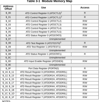
3.2 Module Memory Map
Table 3-1 gives an overview on all ATD_10B8C registers.
[image:13.595.104.491.210.607.2]NOTE: Register Address = Base Address + Address Offset, where the Base Address is defined at the MCU level and the Address Offset is defined at the module level.
Table 3-1 Module Memory Map Address
Offset Use Access
$_00 ATD Control Register 0 (ATDCTL0)1
NOTES:
1. ATDCTL0 is intended for factory test purposes only.
R $_01 ATD Control Register 1 (ATDCTL1)2
2. ATDCTL1 is intended for factory test purposes only.
R
$_02 ATD Control Register 2 (ATDCTL2) R/W
$_03 ATD Control Register 3 (ATDCTL3) R/W
$_04 ATD Control Register 4 (ATDCTL4) R/W
$_05 ATD Control Register 5 (ATDCTL5) R/W
$_06 ATD Status Register 0 (ATDSTAT0) R/W
$_07 Unimplemented
$_08 ATD Test Register 0 (ATDTEST0)3
3. ATDTEST0 is intended for factory test purposes only.
R
$_09 ATD Test Register 1 (ATDTEST1) R/W
$_0A Unimplemented
$_0B ATD Status Register 1 (ATDSTAT1) R
$_0C Unimplemented
$_0D ATD Input Enable Register (ATDDIEN) R/W
$_0E Unimplemented
$_0F Port Data Register (PORTAD) R
3.3 Register Descriptions
This section describes in address order all the ATD_10B8C registers and their individual bits.
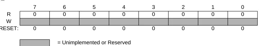
[image:14.595.82.518.170.243.2]3.3.1 Reserved Register (ATDCTL0)
Figure 3-1 Reserved Register (ATDCTL0)
Read: always read $00 in normal modes
Write: unimplemented in normal modes
3.3.2 Reserved Register (ATDCTL1)
Figure 3-2 Reserved Register (ATDCTL1)
Read: always read $00 in normal modes
Write: unimplemented in normal modes
NOTE: Writing to this registers when in special modes can alter functionality.
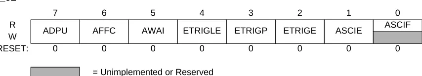
3.3.3 ATD Control Register 2 (ATDCTL2)
This register controls power down, interrupt and external trigger. Writes to this register will abort current conversion sequence but will not start a new sequence.
$_00
7 6 5 4 3 2 1 0
R 0 0 0 0 0 0 0 0
W
RESET: 0 0 0 0 0 0 0 0
= Unimplemented or Reserved
$_01
7 6 5 4 3 2 1 0
R 0 0 0 0 0 0 0 0
W
RESET: 0 0 0 0 0 0 0 0
[image:14.595.85.525.392.470.2]Figure 3-3 ATD Control Register 2 (ATDCTL2) Read: anytime
Write: anytime
ADPU — ATD Power Down
This bit provides on/off control over the ATD_10B8C block allowing reduced MCU power consumption. Because analog electronic is turned off when powered down, the ATD requires a recovery time period after ADPU bit is enabled.
1 = Normal ATD functionality 0 = Power down ATD
AFFC — ATD Fast Flag Clear All
1 = Changes all ATD conversion complete flags to a fast clear sequence. Any access to a result register will cause the associate CCF flag to clear automatically.
0 = ATD flag clearing operates normally (read the status register ATDSTAT1 before reading the result register to clear the associate CCF flag).
AWAI — ATD Power Down in Wait Mode
When entering Wait Mode this bit provides on/off control over the ATD_10B8C block allowing reduced MCU power. Because analog electronic is turned off when powered down, the ATD requires a recovery time period after exit from Wait mode.
1 = Halt conversion and power down ATD during Wait mode
After exiting Wait mode with an interrupt conversion will resume. But due to the recovery time the result of this conversion should be ignored.
0 = ATD continues to run in Wait mode
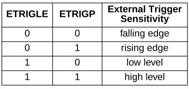
ETRIGLE — External Trigger Level/Edge Control
This bit controls the sensitivity of the external trigger signal. SeeTable 3-2 for details. ETRIGP — External Trigger Polarity
This bit controls the polarity of the external trigger signal. SeeTable 3-2 for details. $_02
7 6 5 4 3 2 1 0
R
ADPU AFFC AWAI ETRIGLE ETRIGP ETRIGE ASCIE ASCIF
W
RESET: 0 0 0 0 0 0 0 0
ETRIGE — External Trigger Mode Enable
This bit enables the external trigger on ATD channel 7. The external trigger allows to synchronize sample and ATD conversions processes with external events.
1 = Enable external trigger 0 = Disable external trigger
NOTE: The conversion results for the external trigger ATD channel 7 have no meaning while external trigger mode is enabled.
ASCIE — ATD Sequence Complete Interrupt Enable
1 = ATD Interrupt will be requested whenever ASCIF=1 is set. 0 = ATD Sequence Complete interrupt requests are disabled.
ASCIF — ATD Sequence Complete Interrupt Flag
If ASCIE=1 the ASCIF flag equals the SCF flag (see3.3.7), else ASCIF reads zero. Writes have no effect.
1 = ATD sequence complete interrupt pending 0 = No ATD interrupt occurred
3.3.4 ATD Control Register 3 (ATDCTL3)
[image:16.595.200.395.81.173.2]This register controls the conversion sequence length, FIFO for results registers and behavior in Freeze Mode. Writes to this register will abort current conversion sequence but will not start a new sequence.
Figure 3-4 ATD Control Register 3 (ATDCTL3)
Read: anytime
[image:16.595.81.517.533.609.2]Write: anytime
Table 3-2 External Trigger Configurations ETRIGLE ETRIGP External TriggerSensitivity
0 0 falling edge
0 1 rising edge
1 0 low level
1 1 high level
$_03
7 6 5 4 3 2 1 0
R 0
S8C S4C S2C S1C FIFO FRZ1 FRZ0
W
RESET: 0 0 1 0 0 0 0 0
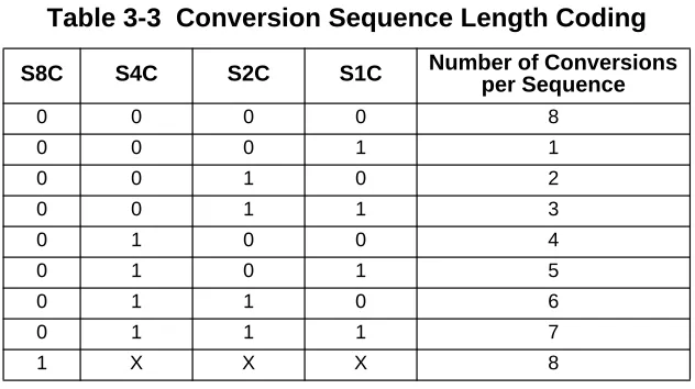
S8C, S4C, S2C, S1C — Conversion Sequence Length
These bits control the number of conversions per sequence.Table 3-3 shows all combinations. At reset, S4C is set to 1 (sequence length is 4). This is to maintain software continuity to HC12 family.
FIFO — Result Register FIFO Mode
If this bit is zero (non-FIFO mode), the A/D conversion results map into the result registers based on the conversion sequence; the result of the first conversion appears in the first result register, the second result in the second result register, and so on.
If this bit is one (FIFO mode) the conversion counter is not reset at the beginning or end of a conversion sequence; conversion results are placed in consecutive result registers between sequences. The result register counter wraps around when it reaches the end of the result register file. The conversion counter value in ATDSTAT0 can be used to determine where in the result register file, the current conversion result will be placed.
Finally, which result registers hold valid data can be tracked using the conversion complete flags. Fast flag clear mode may or may not be useful in a particular application to track valid data.
1 = Conversion results are placed in consecutive result registers (wrap around at end).
0 = Conversion results are placed in the corresponding result register up to the selected sequence length.
FRZ1, FRZ0 — Background Debug Freeze Enable
[image:17.595.140.456.124.301.2]When debugging an application, it is useful in many cases to have the ATD pause when a breakpoint (Freeze Mode) is encountered. These 2 bits determine how the ATD will respond to a breakpoint as shown inTable 3-4. Leakage onto the storage node and comparator reference capacitors may compromise the accuracy of an immediately frozen conversion depending on the length of the freeze period.
Table 3-3 Conversion Sequence Length Coding S8C S4C S2C S1C Number of Conversionsper Sequence
0 0 0 0 8
0 0 0 1 1
0 0 1 0 2
0 0 1 1 3
0 1 0 0 4
0 1 0 1 5
0 1 1 0 6
0 1 1 1 7
1 X X X 8
Table 3-4 ATD Behavior in Freeze Mode (breakpoint)
FRZ1 FRZ0 Behavior in Freeze mode
3.3.5 ATD Control Register 4 (ATDCTL4)
[image:18.595.95.473.63.139.2]This register selects the conversion clock frequency, the length of the second phase of the sample time and the resolution of the A/D conversion (i.e.: 8-bits or 10-bits). Writes to this register will abort current conversion sequence but will not start a new sequence.
Figure 3-5 ATD Control Register 4 (ATDCTL4)
Read: anytime
Write: anytime
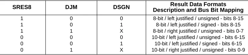
SRES8 — A/D Resolution Select
This bit selects the resolution of A/D conversion results as either 8 or 10 bits. The A/D converter has an accuracy of 10 bits; however, if low resolution is required, the conversion can be speeded up by selecting 8-bit resolution.
1 = 8 bit resolution 0 = 10 bit resolution
SMP1, SMP0 — Sample Time Select
These two bits select the length of the second phase of the sample time in units of ATD conversion clock cycles. Note that the ATD conversion clock period is itself a function of the prescaler value (bits PRS4-0). The sample time consists of two phases. The first phase is two ATD conversion clock cycles long and transfers the sample quickly (via the buffer amplifier) onto the A/D machine’s storage node. The second phase attaches the external analog signal directly to the storage node for final charging and high accuracy.Table 3-5 lists the lengths available for the second sample phase.
0 1 Reserved
1 0 Finish current conversion, then freeze
1 1 Freeze Immediately
$_04
7 6 5 4 3 2 1 0
R
SRES8 SMP1 SMP0 PRS4 PRS3 PRS2 PRS1 PRS0
W
RESET: 0 0 0 0 0 1 0 1
= Unimplemented or Reserved
Table 3-5 Sample Time Select
SMP1 SMP0 Length of 2nd phase of sample time
0 0 2 A/D conversion clock periods
Table 3-4 ATD Behavior in Freeze Mode (breakpoint)
[image:18.595.80.520.237.326.2]PRS4, PRS3, PRS2, PRS1, PRS0 — ATD Clock Prescaler
These 5 bits are the binary value prescaler value PRS. The ATD conversion clock frequency is calculated as follows:
Note that the maximum ATD conversion clock frequency is half the Bus Clock. The default (after reset) prescaler value is 5 which results in a default ATD conversion clock frequency that is Bus Clock divided by 12.Table 3-6 illustrates the divide-by operation and the appropriate range of the Bus Clock.
0 1 4 A/D conversion clock periods
1 0 8 A/D conversion clock periods
[image:19.595.80.477.70.142.2]1 1 16 A/D conversion clock periods
Table 3-6 Clock Prescaler Values Prescale Value Total Divisor
Value Max. Bus Clock1 Min. Bus Clock2
00000 00001 00010 00011 00100 00101 00110 00111 01000 01001 01010 01011 01100 01101 01110 01111 10000 10001 10010 10011 10100 10101 10110 10111 11000 11001 11010 11011 11100 11101 11110 11111
divide by 2 divide by 4 divide by 6 divide by 8 divide by 10 divide by 12 divide by 14 divide by 16 divide by 18 divide by 20 divide by 22 divide by 24 divide by 26 divide by 28 divide by 30 divide by 32 divide by 34 divide by 36 divide by 38 divide by 40 divide by 42 divide by 44 divide by 46 divide by 48 divide by 50 divide by 52 divide by 54 divide by 56 divide by 58 divide by 60 divide by 62 divide by 64
[image:19.595.99.502.310.710.2]4 MHz 8 MHz 12 MHz 16 MHz 20 MHz 24 MHz 28 MHz 32 MHz 36 MHz 40 MHz 44 MHz 48 MHz 52 MHz 56 MHz 60 MHz 64 MHz 68 MHz 72 MHz 76 MHz 80 MHz 84 MHz 88 MHz 92 MHz 96 MHz 100 MHz 104 MHz 108 MHz 112 MHz 116 MHz 120 MHz 124 MHz 128 MHz 1 MHz 2 MHz 3 MHz 4 MHz 5 MHz 6 MHz 7 MHz 8 MHz 9 MHz 10 MHz 11 MHz 12 MHz 13 MHz 14 MHz 15 MHz 16 MHz 17 MHz 18 MHz 19 MHz 20 MHz 21 MHz 22 MHz 23 MHz 24 MHz 25 MHz 26 MHz 27 MHz 28 MHz 29 MHz 30 MHz 31 MHz 32 MHz Table 3-5 Sample Time Select
SMP1 SMP0 Length of 2nd phase of sample time
ATDclock [BusClock] PRS+1
[ ]
NOTE:
1. Maximum ATD conversion clock frequency is 2MHz. The maximum allowed Bus Clock frequency is shown in this column. 2. Minimum ATD conversion clock frequency is 500KHz. The minimum allowed Bus Clock frequency is shown in this column.
3.3.6 ATD Control Register 5 (ATDCTL5)
[image:20.595.79.519.192.280.2]This register selects the type of conversion sequence and the analog input channels sampled. Writes to this register will abort current conversion sequence and start a new conversion sequence.
Figure 3-6 ATD Control Register 5 (ATDCTL5) Read: anytime
Write: anytime
DJM — Result Register Data Justification
This bit controls justification of conversion data in the result registers. See 3.3.13 ATD Conversion
Result Registers (ATDDRHx/ATDDRLx) for details.
1 = Right justified data in the result registers 0 = Left justified data in the result registers
DSGN — Result Register Data Signed or Unsigned Representation
This bit selects between signed and unsigned conversion data representation in the result registers. Signed data is represented as 2’s complement. Signed data is not available in right justification. See
3.3.13 ATD Conversion Result Registers (ATDDRHx/ATDDRLx) for details.
1 = Signed data representation in the result registers 0 = Unsigned data representation in the result registers
Table 3-7 summarizes the result data formats available and how they are set up using the control bits. Table 3-8 illustrates the difference between the signed and unsigned, left justified output codes for an input signal range between 0 and 5.12 Volts.
$_05
7 6 5 4 3 2 1 0
R
DJM DSGN SCAN MULT 0 CC CB CA
W
RESET: 0 0 0 0 0 0 0 0
SCAN — Continuous Conversion Sequence Mode
This bit selects whether conversion sequences are performed continuously or only once. 1 = Continuous conversion sequences (scan mode)
0 = Single conversion sequence
MULT — Multi-Channel Sample Mode
When MULT is 0, the ATD sequence controller samples only from the specified analog input channel for an entire conversion sequence. The analog channel is selected by channel selection code (control bits CC/CB/CA located in ATDCTL5). When MULT is 1, the ATD sequence controller samples across channels. The number of channels sampled is determined by the sequence length value (S8C, S4C, S2C, S1C). The first analog channel examined is determined by channel selection code (CC, CB, CA control bits); subsequent channels sampled in the sequence are determined by incrementing the channel selection code.
1 = Sample across several channels 0 = Sample only one channel
CC, CB, CA — Analog Input Channel Select Code
[image:21.595.82.512.91.187.2]These bits select the analog input channel(s) whose signals are sampled and converted to digital codes. Table 3-9 lists the coding used to select the various analog input channels. In the case of single channel scans (MULT=0), this selection code specified the channel examined. In the case of
Table 3-7 Available Result Data Formats
SRES8 DJM DSGN Description and Bus Bit MappingResult Data Formats
1 1 1 0 0 0 0 0 1 0 0 1 0 1 X 0 1 X
8-bit / left justified / unsigned - bits 8-15 8-bit / left justified / signed - bits 8-15 8-bit / right justified / unsigned - bits 0-7 10-bit / left justified / unsigned - bits 6-15
[image:21.595.91.506.223.378.2]10-bit / left justified / signed - bits 6-15 10-bit / right justified / unsigned - bits 0-9
Table 3-8 Left Justified, Signed and Unsigned ATD Output Codes. Input Signal
Vrl = 0 Volts Vrh = 5.12 Volts
multi-channel scans (MULT=1), this selection code represents the first channel to be examined in the conversion sequence. Subsequent channels are determined by incrementing channel selection code; selection codes that reach the maximum value wrap around to the minimum value.
3.3.7 ATD Status Register 0 (ATDSTAT0)
[image:22.595.131.462.122.284.2]This read-only register contains the Sequence Complete Flag, overrun flags for external trigger and FIFO mode, and the conversion counter.
Figure 3-7 ATD Status Register 0 (ATDSTAT0)
Read: anytime
Write: anytime (No effect on (CC2, CC1, CC0))
SCF — Sequence Complete Flag
This flag is set upon completion of a conversion sequence. If conversion sequences are continuously performed (SCAN=1), the flag is set after each one is completed. This flag is cleared when one of the following occurs:
A) Write “1” to SCF
B) Write to ATDCTL5 (a new conversion sequence is started) C) If AFFC=1 and read of a result register
[image:22.595.82.520.405.485.2]1 = Conversion sequence has completed
Table 3-9 Analog Input Channel Select Coding
CC CB CA Analog InputChannel
0 0 0 AN0
0 0 1 AN1
0 1 0 AN2
0 1 1 AN3
1 0 0 AN4
1 0 1 AN5
1 1 0 AN6
1 1 1 AN7
$_06
7 6 5 4 3 2 1 0
R
SCF 0 ETORF FIFOR 0 CC2 CC1 CC0
W
RESET: 0 0 0 0 0 0 0 0
0 = Conversion sequence not completed
ETORF — External Trigger Overrun Flag
While in edge trigger mode (ETRIGLE=0), if additional active edges are detected while a conversion sequence is in process the overrun flag is set. This flag is cleared when one of the following occurs: A) Write “1” to ETORF
B) Write to ATDCTL2, ATDCTL3 or ATDCTL4 (a conversion sequence is aborted) C) Write to ATDCTL5 (a new conversion sequence is started)
1 = External trigger over run error has occurred 0 = No External trigger over run error has occurred
FIFOR - FIFO Over Run Flag.
This bit indicates that a result register has been written to before its associated conversion complete flag (CCF) has been cleared. This flag is most useful when using the FIFO mode because the flag potentially indicates that result registers are out of sync with the input channels. However, it is also practical for non-FIFO modes, and indicates that a result register has been over written before it has been read (i.e. the old data has been lost). This flag is cleared when one of the following occurs: A) Write “1” to FIFOR
B) Start a new conversion sequence (write to ATDCTL5 or external trigger) 1 = An over run condition exists
0 = No over run has occurred
CC2, CC1, CC0 — Conversion Counter
These 3 read-only bits are the binary value of the conversion counter. The conversion counter points to the result register that will receive the result of the current conversion. E.g. CC2=1, CC1=1, CC0=0 indicates that the result of the current conversion will be in ATD Result Register 6. If in non-FIFO mode (FIFO=0) the conversion counter is initialized to zero at the begin and end of the conversion sequence. If in FIFO mode (FIFO=1) the register counter is not initialized. The conversion counters wraps around when its maximum value is reached.
[image:23.595.87.513.521.614.2]3.3.8 Reserved Register (ATDTEST0)
Figure 3-8 Reserved Register (ATDTEST0) Read: anytime, returns unpredictable values
Write: anytime in special modes, unimplemented in normal modes $_08
7 6 5 4 3 2 1 0
R U U U U U U U U
W
RESET: 1 0 0 0 0 0 0 0
NOTE: Writing to this registers when in special modes can alter functionality.
3.3.9 ATD Test Register 1 (ATDTEST1)
[image:24.595.82.519.157.233.2]This register contains the SC bit used to enable special channel conversions.
Figure 3-9 ATD Test Register 1 (ATDTEST1) Read: anytime, returns unpredictable values for Bit7 and Bit6
Write: anytime
SC - Special Channel Conversion Bit
If this bit is set, then special channel conversion can be selected using CC, CB and CA of ATDCTL5. Table 3-10 lists the coding.
1 = Special channel conversions enabled 0 = Special channel conversions disabled
NOTE: Always write remaining bits of ATDTEST1 (Bit7 to Bit1) zero when writing SC bit. Not doing so might result in unpredictable ATD behavior.
3.3.10 ATD Status Register 1 (ATDSTAT1)
This read-only register contains the Conversion Complete Flags. $_09
7 6 5 4 3 2 1 0
R U U 0 0 0 0 0
SC W
RESET: 0 0 0 0 0 0 0 0
[image:24.595.105.493.476.591.2]= Unimplemented or Reserved
Table 3-10 Special Channel Select Coding
SC CC CB CA Analog InputChannel
1 0 X X Reserved
1 1 0 0 VRH
1 1 0 1 VRL
1 1 1 0 (VRH+VRL) / 2
Figure 3-10 ATD Status Register 1 (ATDSTAT1) Read: anytime
Write: anytime, no effect
CCFx — Conversion Complete Flag x (x=7,6,5,4,3,2,1,0)
A conversion complete flag is set at the end of each conversion in a conversion sequence. The flags are associated with the conversion position in a sequence (and also the result register number). Therefore, CCF0 is set when the first conversion in a sequence is complete and the result is available in result register ATDDR0; CCF1 is set when the second conversion in a sequence is complete and the result is available in ATDDR1, and so forth. A flag CCFx (x=7,6,5,4,3,2,1,0) is cleared when one of the following occurs:
A) Write to ATDCTL5 (a new conversion sequence is started)
B) If AFFC=0 and read of ATDSTAT1 followed by read of result register ATDDRx C) If AFFC=1 and read of result register ATDDRx
1 = Conversion number x has completed, result ready in ATDDRx 0 = Conversion number x not completed
3.3.11 ATD Input Enable Register (ATDDIEN)
Figure 3-11 ATD Input Enable Register (ATDDIEN) Read: anytime
Write: anytime
IENx — ATD Digital Input Enable on channel x (x= 7, 6, 5, 4, 3, 2, 1, 0)
This bit controls the digital input buffer from the analog input pin (ANx) to PTADx data register. 1 = Enable digital input buffer to PTADx.
$_0B
7 6 5 4 3 2 1 0
R CCF7 CCF6 CCF5 CCF4 CCF3 CCF2 CCF1 CCF0
W
RESET: 0 0 0 0 0 0 0 0
= Unimplemented or Reserved
$_0D
7 6 5 4 3 2 1 0
R
IEN7 IEN6 IEN5 IEN4 IEN3 IEN2 IEN1 IEN0
W
RESET: 0 0 0 0 0 0 0 0
[image:25.595.82.517.487.560.2]0 = Disable digital input buffer to PTADx
NOTE: Setting this bit will enable the corresponding digital input buffer continuously. If this bit is set while simultaneously using it as an analog port, there is potentially increased power consumption because the digital input buffer maybe in the linear region.
3.3.12 Port Data Register (PORTAD)
[image:26.595.80.517.237.355.2]The data port associated with the ATD is input-only. The port pins are shared with the analog A/D inputs AN7-0.
Figure 3-12 Port Data Register (PORTAD) Read: anytime
Write: anytime, no effect
The A/D input channels may be used for general purpose digital input.
PTADx — A/D Channel x (ANx) Digital Input (x= 7,6,5,4,3,2,1,0)
If the digital input buffer on the ANx pin is enabled (IENx=1) read returns the logic level on ANx pin (signal potentials not meeting VIL or VIH specifications will have an indeterminate value)).
If the digital input buffers are disabled (IENx=0), read returns a “1”.
Reset sets all PORTAD bits to “1”.
3.3.13 ATD Conversion Result Registers (ATDDRHx/ATDDRLx)
The A/D conversion results are stored in 8 read-only result registers ATDDRHx/ATDDRLx. The result data is formatted in the result registers based on two criteria. First there is left and right justification; this selection is made using the DJM control bit in ATDCTL5. Second there is signed and unsigned data; this selection is made using the DSGN control bit in ATDCTL5. Signed data is stored in 2’s complement format and only exists in left justified format. Signed data selected for right justified format is ignored.
Read: anytime
Write: anytime, no effect in normal modes $_0F
7 6 5 4 3 2 1 0
R PTAD7 PTAD6 PTAD5 PTAD4 PTAD3 PTAD2 PTAD1 PTAD0
W
RESET: 1 1 1 1 1 1 1 1
Pin
Func-tion
AN7 AN6 AN5 AN4 AN3 AN2 AN1 AN0
3.3.13.1 Left Justified Result Data
[image:27.595.58.535.251.352.2]Figure 3-13 Left Justified, ATD Conversion Result Register, High Byte (ATDDRxH)
Figure 3-14 Left Justified, ATD Conversion Result Register, Low Byte (ATDDRxL) 3.3.13.2 Right Justified Result Data
Figure 3-15 Right Justified, ATD Conversion Result Register, High Byte (ATDDRxH) $_10 = ATDDR0H, $_12 = ATDDR1H, $_14 = ATDDR2H, $_16 = ATDDR3H
$_18 = ATDDR4H, $_1A = ATDDR5H, $_1C = ATDDR6H, $_1E = ATDDR7H
7 6 5 4 3 2 1 0
R BIT 9 MSB BIT 7 MSB
BIT 8 BIT 6 BIT 7 BIT 5 BIT 6 BIT 4 BIT 5 BIT 3 BIT 4 BIT 2 BIT 3 BIT 1 BIT 2 BIT 0 10-bit data 8-bit data W
RESET: 0 0 0 0 0 0 0 0
= Unimplemented or Reserved
$_11 = ATDDR0L, $_13 = ATDDR1L, $_15 = ATDDR2L, $_17 = ATDDR3L $_19 = ATDDR4L, $_1B = ATDDR5L, $_1D = ATDDR6L, $_1F = ATDDR7L
7 6 5 4 3 2 1 0
R BIT 1
U BIT 0 U 0 0 0 0 0 0 0 0 0 0 0 0 10-bit data 8-bit data W
RESET: 0 0 0 0 0 0 0 0
= Unimplemented or Reserved
$_10 = ATDDR0H, $_12 = ATDDR1H, $_14 = ATDDR2H, $_16 = ATDDR3H $_18 = ATDDR4H, $_1A = ATDDR5H, $_1C = ATDDR6H, $_1E = ATDDR7H
7 6 5 4 3 2 1 0
R 0 0 0 0 0 0 0 0 0 0 0 0
BIT 9 MSB 0 BIT 8 0 10-bit data 8-bit data W
RESET: 0 0 0 0 0 0 0 0
[image:27.595.58.545.433.537.2]Figure 3-16 Right Justified, ATD Conversion Result Register, Low Byte (ATDDRxL) $_11 = ATDDR0L, $_13 = ATDDR1L, $_15 = ATDDR2L, $_17 = ATDDR3L
$_19 = ATDDR4L, $_1B = ATDDR5L, $_1D = ATDDR6L, $_1F = ATDDR7L
7 6 5 4 3 2 1 0
R BIT 7
BIT 7 MSB
BIT 6 BIT 6
BIT 5 BIT 5
BIT 4 BIT 4
BIT 3 BIT 3
BIT 2 BIT 2
BIT 1 BIT 1
BIT 0 BIT 0
10-bit data 8-bit data W
RESET: 0 0 0 0 0 0 0 0
Section 4 Functional Description
4.1 General
The ATD_10B8C is structured in an analog and a digital sub-block.
4.2 Analog Sub-block
The analog sub-block contains all analog electronics required to perform a single conversion. Separate power supplies VDDA and VSSA allow to isolate noise of other MCU circuitry from the analog sub-block.
4.2.1 Sample and Hold Machine
The Sample and Hold (S/H) Machine accepts analog signals from the external surroundings and stores them as capacitor charge on a storage node.
The sample process uses a two stage approach. During the first stage, the sample amplifier is used to quickly charge the storage node.The second stage connects the input directly to the storage node to complete the sample for high accuracy.
When not sampling, the sample and hold machine disables its own clocks. The analog electronics still draw their quiescent current. The power down (ADPU) bit must be set to disable both the digital clocks and the analog power consumption.
The input analog signals are unipolar and must fall within the potential range of VSSA to VDDA.
4.2.2 Analog Input Multiplexer
The analog input multiplexer connects one of the 8 external analog input channels to the sample and hold machine.
4.2.3 Sample Buffer Amplifier
The sample amplifier is used to buffer the input analog signal so that the storage node can be quickly charged to the sample potential.
4.2.4 Analog-to-Digital (A/D) Machine
When not converting the A/D machine disables its own clocks. The analog electronics still draws quiescent current. The power down (ADPU) bit must be set to disable both the digital clocks and the analog power consumption.
Only analog input signals within the potential range of VRLto VRH(A/D reference potentials) will result in a non-railed digital output codes.
4.3 Digital Sub-block
This subsection explains some of the digital features in more detail. See register descriptions for all details.
4.3.1 External Trigger Input (ETRIG)
[image:30.595.106.490.336.573.2]The external trigger feature allows the user to synchronize ATD conversions to the external environment events rather than relying on software to signal the ATD module when ATD conversions are to take place. The input signal (ATD channel 7) is programmable to be edge or level sensitive with polarity control. Table 4-1 gives a brief description of the different combinations of control bits and their affect on the external trigger function.
During a conversion, if additional active edges are detected the overrun error flag ETORF is set.
In either level or edge triggered modes, the first conversion begins when the trigger is received. In both cases, the maximum latency time is one Bus Clock cycle plus any skew or delay introduced by the trigger circuitry.
[image:30.595.108.488.340.570.2]NOTE: The conversion results for the external trigger ATD channel 7 have no meaning while external trigger mode is enabled.
Table 4-1 External Trigger Control Bits
ETRIGLE ETRIGP ETRIGE SCAN Description
X X 0 0 Ignores external trigger. Performs one conversion sequence and stops.
X X 0 1 Ignores external trigger. Performs
continuous conversion sequences.
0 0 1 X Falling edge triggered. Performs one
conversion sequence per trigger.
0 1 1 X Rising edge triggered. Performs one
conversion sequence per trigger.
1 0 1 X
Trigger active low. Performs
continuous conversions while trigger is active.
1 1 1 X
Once ETRIGE is enabled, conversions cannot be started by a write to ATDCTL5, but rather must be triggered externally.
If the level mode is active and the external trigger both de-asserts and re-asserts itself during a conversion sequence, this does not constitute an overrun; therefore, the flag is not set. If the trigger is left asserted in level mode while a sequence is completing, another sequence will be triggered immediately.
4.3.2 General Purpose Digital Input Port Operation
The input channel pins can be multiplexed between analog and digital data. As analog inputs, they are multiplexed and sampled to supply signals to the A/D converter. As digital inputs, they supply external input data that can be accessed through the digital port register PORTAD (input-only).
The analog/digital multiplex operation is performed in the input pads. The input pad is always connected to the analog inputs of the ATD_10B8C. The input pad signal is buffered to the digital port registers. This buffer can be turned on or off with the ATDDIEN register. This is important so that the buffer does not draw excess current when analog potentials are presented at its input.
4.3.3 Low Power Modes
The ATD_10B8C can be configured for lower MCU power consumption in 3 different ways:
• Stop Mode: This halts A/D conversion. Exit from Stop mode will resume A/D conversion, But due to the recovery time the result of this conversion should be ignored.
• Wait Mode with AWAI=1: This halts A/D conversion. Exit from Wait mode will resume A/D conversion, but due to the recovery time the result of this conversion should be ignored.
• Writing ADPU=0 (Note that all ATD registers remain accessible.): This aborts any A/D conversion in progress.
Section 5 Resets
5.1 General
Section 6 Interrupts
6.1 General
The interrupt requested by the ATD_10B8C is listed inTable 6-1. Refer to MCU specification for related vector address and priority.
[image:35.595.161.438.172.256.2]See register descriptions for further details.
Table 6-1 ATD_10B8C Interrupt Vectors Interrupt Source CCR
Mask Local Enable
Sequence Complete
FINAL PAGE OF
38