FPGA Implimentation of DSSS Transmitter Using
Pseudo Chaotic Sequence
Nandini A. Gumgaokar1, Kalyani G. Joshi2, Vaishnavi S. Joshi3 SumatiJagdale4,
1, 2, 3, 4
Dept of ENTC Engineering, Bvcoewpune, India,
Abstract: The interference problems associated with narrow-band very high frequency and ultra high frequency Data transfer systems are reduced by a new data transfer technology known as Spread spectrum (SS) technology[1]. Spread spectrum technology provides strong secure communication & reduces mixing of communication. In this paper we specified the design of DSSS (Direct Sequence Spread Spectrum) transmitter. The Pseudo Chaotic Sequence generator and DSSS is implemented in FPGA (Field Programmable Gate Array). The generated pseudo chaotic sequences are investigated for autocorrelation, cross correlation & balance properties[3].
Keywords: Digital communication, spread spectrum, pseudo noise, chaos, chaotic sequence generator.
I. INTRODUCTION
In spread spectrum communication systems, Pseudo noise sequence is used to spread the bandwidth of transmitting signal. The properties of pseudo noise sequence which are autocorrelation and cross correlation are very important in spread spectrum communication[1]. This paper includes study of a completely different type of spreading sequence for use in DSSS system. Therefore in the past 30 years, there has been a great deal of interest in study of non-linear systems which develop chaos sequence. So, in this paper we have used PCS sequence instead of PN sequence[2] . Because there are various drawbacks of PN sequence. By using PCS sequence sequence, we can spread the bandwidth in larger amount.
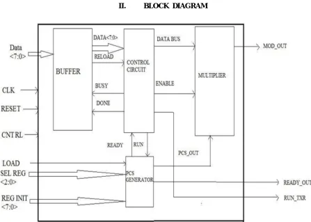
[image:1.612.81.528.399.718.2]II. BLOCK DIAGRAM
A. Block Diagram Discription
There are four main blocks present in the DSSS transmitter which are Buffer, Control circuit, Multiplier, PCS generator. The main block of this project is PCS generator. There are 3 input signals given to this PCS generator. The registers of 8 bits are loaded by the LOAD=1 signal. We use the 3 bits of register for further operations. Those 3 bits are selected by the SEL register and given to the PCS generator. The tracking and synchronisation of receiver can be done easily by sending 8 bit data as ‘11111111’. When the register values are loaded into PCS generator, it will send READY=1signal to the control circuit to start the its own operation. If control circuit is busy then it will send the BUSY=1 & DONE=0 signal to the buffer. When control circuit becomes free it will send BUSY=0 & DONE=1 signal to buffer.Buffer will be used to store the register data. That data is stored in the buffer register of the control circuit. After this control circuit send RUN=1 signal to PCS signal to send next 8 bit values for operation. The data stored in the control circuit is given to the multiplier block by using DATA BUS signal. Multiplier also get the 32 bits of data from the PCS generator. The sequence of 8 bit came from control circuit and 32 bits sequence came from PCS generator is multiplied and we get the output sequence of 256 bits at the output.
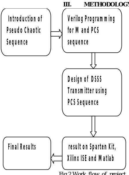
III. METHODOLOGY
Introduction of
Pseudo Chaotic
Sequence
Verilog Programming
for M and PCS
sequence
Design of DSSS
Transmitter using
PCS Sequence
[image:2.612.146.370.244.548.2]result on Sparten Kit,
Xilinx ISE and Matlab
Final Results
Fig 2.Work flow of project
B. PCS Sequence
PCS generates a pseudo chaotic PN sequence with good cross-correlation and auto-correlation properties that is well suited for DSSS system. Because of long periodicity, it provides very high security and is capable of handling many users.[6]. The PCS generator used consists of four such cells connected in series as shown in Fig.3.4. An exhaustive search was conducted to characterize the length of the sequences generated by the pseudo -chaotic finite state machines. The PCS generator contains eight 8-bit registers. These registers provide a total of 64 binary memory elements. Therefore, the PCS generator can be viewed as a sequential state machine with at most 264 possible states. The initial values to these registers can be initialized individually[3].
C. DSSS System
IV. RESULT
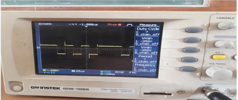
[image:3.612.123.488.84.291.2]Fig 3.when sparten 3a kit is connected to the dso we get the pseudo chaotic sequence as shown in above picture.
Fig 4. All connections are obtained on the fpga sparten 3a kit.
[image:3.612.129.518.537.718.2]Fig 6. above picture shows the spreded sequence when two bits are enabled on fpga kit.
Fig 7. again enable the 4 bits of fpga kit instead of 2 bits to obtain more spreaded sequence on dso.
Fig 8.from above picture we can see that whenever number of bits are increased we get the more secure and spreaded sequence.
A. This system will replace the pseudo random sequence to the Pseudo Chaotic Sequence.
B. Design DSSS transmitter with PCS sequence.
C. After replacing it will spread the pseudo chaotic sequence with the help of DSSS.
REFERENCES
[1] G. Heidari-Bateni ,C.D.McGillem: “chaotic sequences for spread spectrum :An alternative to PN-sequences. Proc. IEEE ICWC-92437C440(1992).
[2] Lehnert J.S. ,Pursley M.B., “Error Probabilities for Binary Direct-sequence spread-spectrum communications with Random Signature Sequences”, IEEE Transactions on communications , January, pp.87—98.
[3] Devaney R.L. ,An Introduction to Chaotic Dynamical Systems, Addison-Wesley publishing Company, Inc. , California, 1989. [4] May R.M., “Special Mathematical Models With Very Complicated Dynamics”, Nature, June 1996.
[5] Schuster H.G., Deterministic Chaos, An Introduction .”Physick-VerlagGmnh, D-6940 Weinheim, Federal Republic Of Germany,1984.