Abstract—First-principles calculations based on the Density Functional Theory (DFT) within the generalized gradient approximation (GGA), and the introduction of intra-atomic interaction term for strongly correlated electrons (DFT+U), have been utilized to study defective SnO2 crystals.
Introduction of some impurities, such as F, Ga, Al and Cr affect the structural, electronic and magnetic properties of tin dioxide. F doping produces alterations in the structure, with Sn atoms moving away from the impurity and O atoms moving closer to it; and, the system presents n-type electrical conductivity. Ga impurity incorporation distorts its surrounding, with the atoms moving closer to the impurity whereas the electrical properties of crystal remain unchanged. Results for Al impurity are almost the same as those for the Ga-doping. Cr-doping produces the atoms in the neighbourhood of the point defect to move towards it, the band gap has been slightly reduced and we observe the occurrence of a local magnetic moment.
Index Terms—SnO2, Impurity doping, DFT, point defects.
I. INTRODUCTION
in oxide (SnO2) is an oxide that belongs to the
so-called transparent conducting oxides (TCOs). It has a direct band-gap which width is equal to 3.6 eV [1]. Its applications among others include solar energy panels, low-emission glasses and heat mirrors [2].
Nature of the properties of the SnO2 crystals depend on
different kind of defects and impurities that are present in the structure of this material. These defects could affect its structural, electronic, optical and/or magnetic properties. That means a strong necessity to understand the nature of the alterations being produced by the point defects in order to succeed in successful application of the tin dioxide. The present work has the purpose to understand better what is happening at the fundamental quantum level in this crystal if some impurities such as fluorine, gallium, aluminium and chromium are incorporated in the otherwise pure material.
Richard Rivera is with the Grupo de Fisicoquímica de Materiales in the Universidad Técnica Particular de Loja, Loja, Ecuador (e-mail: rariverax@utpl.edu.ec)
Freddy Marcillo is with the Grupo de Fisicoquímica de Materiales, and Escuela de Ingeniería Química in the Universidad Técnica Particular de Loja, Loja, Ecuador (e-mail: fpmarcillo@utpl.edu.ec)
Washington Chamba is with the Grupo de Fisicoquímica de Materiales, and Escuela de Ingeniería Química in the Universidad Técnica Particular de Loja, Loja, Ecuador (e-mail: wachamba@utpl.edu.ec)
Patricio Puchaicela is with the Grupo de Fisicoquímica de Materiales in the Universidad Técnica Particular de Loja, Loja, Ecuador (e-mail: ppuchaicela@utpl.edu.ec)
Arvids Stashans is with the Grupo de Fisicoquímica de Materiales in the Universidad Técnica Particular de Loja, Loja. Ecuador (e-mail: arvids@utpl.edu.ec)
II. METHODOLOGY
Vienna ab initio Simulation Package (VASP) [3] has been
used throughout the investigation. It is based on the DFT approach. The interaction between the core electrons and the valence electrons is implemented through the projector augmented wave (PAW) method [4], and additionally the PerdewBurkeErnzerhof (PBE) [5] GGA exchange-correlation functionals are implemented in the work.
A cut-off kinetic energy of 500 eV is used by converging the total energy to less than 1 meV/atom. Γ-centred Monkhorst-Pack (MP) grid with a 0.035 Å-1 separation is
applied, which corresponds to a k-point mesh of 6x6x8 for the 6-atom primitive unit cell of the tin dioxide, SnO2. The
above-mentioned parameters are obtained through the atomic relaxation until all the forces are < 0.008 eV/Å and equilibrium state of the system has been achieved.
DFT theory has difficulties in describing the strong correlation of Sn-d electrons, and, in order to take into
account these issues, an intra-site Coulomb repulsion U
-term has been included. That results in the so-called DFT+U
method [6]. After performing some test calculations, U = 4.0
eV was obtained as a proper value allowing to get a band gap width equal to 1.68 eV. The corresponding experimental value is about 3.6 eV [7], but larger U values have negative
impact on the equilibrium structural parameters, so we refused to enlarge the magnitude of this parameter. The computed lattice parameters have been found to be equal to
a = 4.73 Å and c = 3.16 Å, in close agreement with the
available experimental data [1].
Finally, in order to study the effects of F, Cr and Ga impurities in the SnO2 crystals, 6-atoms primitive unit cell
was expanded sixteen times (2 x 2 x 4 extension), which results in 96-atom supercell, with a k-point mesh of 3x3x2.
TABLEI
CHARGES AND DISPLACEMENTS
Atom Q1(e) Q2(e) ∆R (Å)
F (1) - -0.76 -
Sn (2) 2.41 2.43 0.13
Sn (3) 2.42 2.43 0.16
Sn (4) 2.42 2.43 0.16
O (5) -1.20 -1.21 -0.04
O (6) -1.21 -1.21 -0.04
O (7) -1.21 -1.21 -0.04
O (8) -1.20 -1.21 -0.04
O (9) -1.21 -1.21 -
O (10) -1.21 -1.22 -0.01
O (11) -1.21 -1.22 -0.01
O (12) -1.20 -1.22 -0.01
O (13) -1.21 -1.22 -0.01
SnO
2
Physical and Chemical Properties due to
the Impurity Doping
Richard Rivera, Freddy Marcillo, Washington Chamba, Patricio Puchaicela, Arvids Stashans
1
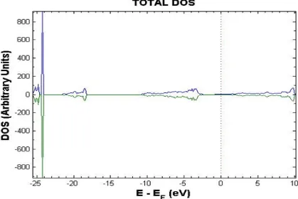
Fig 2. Total DOS of the F-doped SnO2crystal. The dotted line marks the Fermi level (EF).
Charges on atoms obtained by the Bader population analysis for the perfect (Q1) and F-doped (Q2) SnO2 crystals. The atomic displacements
[image:2.612.76.283.107.364.2](ΔR) regarding the impurity for atoms within the defective region are also shown. Positive atomics displacements stand for the defect-outward movements. The atomic numeration corresponds to the one indicated in Fig. 1.
III. RESULTS AND DISCUSSION
A. F-doped SnO2
Fig 1. Atomic displacements in the SnO2 crystalline lattice in the
neighbourhood of the F dopant. The Sn atoms move towards the impurity while the O atoms move outwards the defect.
One of the O atoms situated in the central part of the supercell was replaced by an F atom. As a result of such a
process, the atoms in the neighbourhood of the defective region have a tendency to displace themselves in order to find new equilibrium positions. The Sn atoms move outwards the impurity meanwhile the O atoms have a tendency to move towards the F atom as it is shown in Table I as well as Fig. 1.
In an attempt to explain the reason of these motions, Bader charge analysis [7] has been carried out. These computations show that the charge on the impurity F atom is -0.76 e. The replaced O atom had a charge of -1.21 e in pure
crystal. This means that the Sn atoms move outwards the impurity due to the reduction in the Coulomb electrostatic attraction because of the defect incorporation. Similarly, the O atoms reduce their initial distance until the F atom because of the reduction in the Coulomb repulsion.
Density of States (DOS) pattern is shown in Fig. 2. It is possible to observe that the Fermi level is situated at the bottom of the Conduction Band (CB), which means that the introduction of the F impurity, which brings to the system one extra valence electron, produces electronic state in the CB and leads to the n-type electrical conductivity.
B. Ga-doped SnO2
Ga doping was done by replacing one of the lattice central host Sn atoms by the impurity. The atoms surrounding the impurity move themselves in order to find new equilibrium positions, as it is possible to see in Table II and Fig. 3. All the atoms in the neighbourhood of the impurity reduce their initial distance with respect to the defect. The Bader charge analysis shows that the impurity has a charge of 1.77 e
instead of the 2.41 e for the replaced Sn atom. This means that the Coulomb repulsion to the nearest Sn atoms is smaller, and they have a tendency to move closer to the dopant. O atoms move slightly closer, most likely trying to
[image:2.612.108.527.446.726.2]keep their bond lengths with their nearest Sn atoms.
TABLEII
CHARGES AND DISPLACEMENTS
Atom Q1(e) Q2(e) ∆R (Å)
Ga (1) - 1.77 -
Sn (2) 2.42 2.43 -0.04
Sn (3) 2.42 2.43 -0.04
O (4) -1.21 -1.17 -0.02
O (5) -1.21 -1.17 -0.02
O (6) -1.21 -1.16 -0.02
O (7) -1.21 -1.17 -0.02
O (8) -1.21 -1.17 -0.02
O (9) -1.20 -1.16 -0.02
Charges on atoms obtained by the Bader population analysis for the perfect (Q1) and Ga-doped (Q2) SnO2 crystals. The atomic displacements
[image:3.612.68.295.74.231.2] [image:3.612.313.537.199.357.2](ΔR) regarding the impurity for atoms within the defective region are also shown. Positive atomics displacements stand for the defect-outward movements. The atomic numeration corresponds to the one indicated in Fig. 3.
Fig 3. Atomic displacements in the SnO2 crystalline lattice in the
neighbourhood of the Ga dopant. Both Sn and O atoms have a tendency to move towards the impurity. (Atomic shifts in case of the Al- and Cr-doping are essentially the same).
Fig. 4 shows DOS pattern for this system. Ga atom has some small contributions in the upper Valence Band (VB) and the CB as well. However, there is no presence of any local energy level within the band-gap region, and no changes in band-gap width have been found. That means the presence of the Ga impurity in SnO2 has no notable
influence upon the electrical conductivity in this material.
C. Al-doped SnO2
TABLEIII CHARGES AND DISPLACEMENTS
Atom Q1(e) Q2(e) ∆R (Å)
Al (1) - 2.48 -
Sn (2) 2.42 2.46 -0.07
Sn (3) 2.42 2.46 -0.07
O (4) -1.21 -1.29 -0.09
O (5) -1.21 -1.29 -0.09
O (6) -1.21 -1.26 -0.07
O (7) -1.21 -1.29 -0.09
O (8) -1.21 -1.29 -0.09
O (9) -1.21 -1.26 -0.07
[image:3.612.77.293.290.439.2]Charges on atoms obtained by the Bader population analysis for the perfect (Q1) and Al-doped (Q2) SnO2 crystals. The atomic displacements (ΔR) regarding the impurity for atoms within the defective region are also shown. Positive atomics displacements stand for the defect-outward movements. The atomic numeration corresponds to the one indicated in Fig. 3.
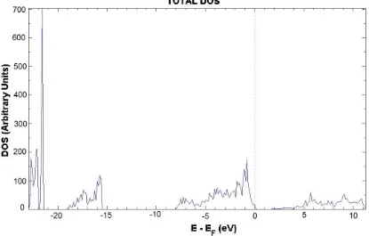
[image:3.612.105.520.470.735.2]
Fig 5. Total DOS of the Al-doped SnO2 crystal. The dotted line marks the Fermi level (EF).
in order to find new equilibrium positions. The obtained relevant atomic displacements are shown in Table III. Generally, atoms move towards the impurity. Bader charge analysis shows that the charge on the dopant is 2.48 e, which
is slightly larger than the charge of the replaced Sn atom (2.41 e) in un-doped material. Despite small change of this
atomics charge, we observe notable charge alterations on the defect-closest atoms. The Sn atoms become more positive whereas the O atoms are more negative. This means that the nature of the chemical bonding has become more ionic, which explains why the O atoms move towards the impurity. The Sn atoms try to preserve their bonds with the O atoms, moving along with them, even if it reduces their distance regarding the dopant.
The DOS (Fig. 5) is practically unchanged due the presence of the Al atom. Impurity atom has some small contributions in the upper VB and the CB, but no presence of any local level has been observed. The band-gap width increases slightly up to 1.78 eV, which means there are no major changes on electrical conductivity.
D. Cr-doped SnO2
Cr doping was done similarly: one of the Sn atoms was replaced by the impurity. In order to describe appropriately the Cr impurity, parameter U = 4.0 eV has been utilized [8].
The introduction of impurity affects its surroundings with local microstructure being altered. Movements of both, Sn and O atoms are towards the impurity (Table IV). Bader charge analysis shows that the charge on the Cr impurity is 2.01 e, which is smaller than the 2.41 e on the replaced Sn
atom. That explains the movements of the Sn atoms: the Coulomb repulsion has decreased. On the other hand, it is found that O atoms also move towards the impurity. In this case, it is necessary to state that the atomic radius of the Cr atom (1.27 Å) is smaller than the corresponding radius of the replaced Sn atom (1.40 Å). That is why due to the impurity incorporation, the bond length is artificially larger than the value it should have according to the atomic radii, and the O atoms are rearranging themselves according to this fact, trying to keep an appropriate bond length with the defect, i.e. moving towards the impurity.
TABLEIV
CHARGES AND DISPLACEMENTS
Atom Q1(e) Q2(e) ∆R (Å)
Cr (1) - 2.01 -
Sn (2) 2.42 2.47 -0.03
Sn (3) 2.42 2.47 -0.03
O (4) -1.21 -1.16 -0.06
O (5) -1.21 -1.16 -0.06
O (6) -1.21 -1.13 -0.09
O (7) -1.21 -1.16 -0.06
O (8) -1.21 -1.16 -0.06
O (9) -1.21 -1.13 -0.09
Charges on atoms obtained by the Bader population analysis for the perfect (Q1) and Cr-doped (Q2) SnO2 crystals. The atomic displacements
(ΔR) regarding the impurity for atoms within the defective region are also shown. Positive atomics displacements stand for the defect-outward movements. The atomic numeration corresponds to the one indicated in Fig. 3.
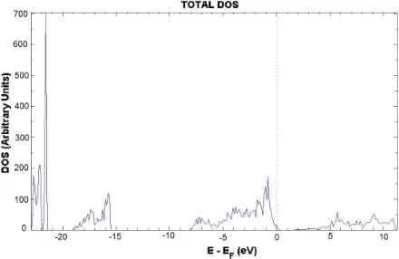
Fig 6. Total DOS of the Cr-doped SnO2 crystal. The dotted line marks the Fermi level (EF).
DOS has been also calculated and is shown in Fig 6. There are no major changes upon the band structure compared to the corresponding DOS picture of the pure crystal. Nevertheless, some contributions of the Cr 5d atomic orbitals (AOs) in the CB for the β spin can be noticed. The band-gap width increases slightly up to 1.85 eV.
Cr doping leads to the occurrence of local magnetic moment in the lattice. The total magnetic moment of supercell is found to be around +2.0 µB, with impurity
contribution being approximately +2.27 µB. Small negative
contributions of defect-nearest O atoms has been also observed.
IV. CONCLUSIONS
A quantum-mechanical study of tin dioxide in the presence of some impurities through the DFT+U approach
has been carried out. The obtained structural parameters are in accordance with the experimental results.
The main conclusions due to the impurity doping can be drawn from the analysis of the obtained results. In case of the F-doping, it is found that the O atoms move towards the F atom whereas the Sn atoms move outwards the defect, due to changes in the electrostatic interaction within the defective region. F substitution leads to the increase in the n-type conductivity.
Ga-doping produces atomic shifts towards the defect. Neither local energy levels within the band-gap region nor changes in the band-gap width are observed.
Al-doping changes slightly the nature of chemical bonding in its neighbourhood. It becomes more ionic due to increase of both positive and negative atomic charges on Sn
and O atoms, respectively. The DOS analysis shows slight increase in band-gap width of the doped material.
The incorporation of a Cr atom produces defect-inward atomic shifts. Cr atom itself has local influence upon the band structure properties of the material with some contributions towards CB for the β spin. Small increase in the band-gap width is also observed. Finally, Cr dopant produces local magnetic moment in the crystalline lattice.
REFERENCES
[1] K. G. Godinho, A. Walsh, G. W. Watson, J Phys. Chem. 113 (2009) 439.
[2] B. Zhang, Y. Tian, J. Zhang, W. Cai, Optelectonics and Advanced Materials-Rapid communications 4 (2010) 1158
[3] G. Kresse, J. Furthmüller, Comput. Mater. Sci. 6 (1996) 15. [4] G. Kresse, D. Joubert, Phys. Rev. B 59 (1999) 1758.
[5] J.P. Perdew, M. Ernzerhof, K. Burke, Phys. Rev. Lett. 77 (1996) 3865.
[6] A.I. Liechtenstein, V.I. Anisimov, J. Zaanen, Phys. Rev. B 52 (1995) 5467.
[7] R.F.W. Bader, The International Series of Monographs on Chemistry 22, Oxford University Press, Oxford, 1990