FPGA based High Speed CRC Encoder and
Decoder
Shraddha Datir1, Dr. R. D. Ghongade2, Dr. C. J. Shelke3
1
ME Student, HOD, E&TC, PRPCEM, AMRAVATI, 3
(HOD, IT, PRPCET, AMRAVATI)
Abstract: Cyclic redundancy check (CRC) technique is one of the most efficient error detection method, which used to detect single and burst errors. CRC method adds redundancy bits to the original data. The reminder of division between original message and selected polynomial is represents redundancy bit. At the receiver side, the received data can be recognized as valid or not. Generally speaking, (CRCs) are used to detect errors from noise in digital data transmission. The technique is also sometimes applied to data storage devices, such as a disk drive. They also have been turned to verify the integrity of files in a system in order to prevent tampering and suggested as a possible algorithm for manipulation detection codes .A Cyclic Redundancy Check (CRC) is the remainder or residue of binary division of a potentially long message, by a CRC polynomial. Per packet operation is necessary for IP protocol, design a new efficient technique using FPGA in case of CRC .This approach is memory efficient and operate at high speed, since most of method currently employed based on look up table consume more time ,more space and also there will be a ROM which stores the look up table. This paper presents high speed CRC encoder and decoder using FIELD PROGRAMMABLE GATE ARRAY, to increase throughput pipeline method is used. Also reduced time required to transmission, which improved speed of communication.
Keywords: CRC Encoder, CRC Decoder, XOR, Encryption, Decryption, FPGA, serial CRC, parallel CRC, etc
I. INTRODUCTION
1) Serial CRC Generation: Here CRC checking is done serially. The data input will be single (binary) and every clock pulse the data input will be one. There will some delay present between the consecutive data inputs and the output will be zero if the data will be encoded with same CRC value otherwise it shows non-zero value. The data is serially processed; the polynomial is XOR with the data input, that will be given to the D flip-flop (output same as the input) final CRC is generated as serially.
2) Parallel CRC Generation: Every modern communication protocol uses one or more error-detection algorithms. CRC is by far the most popular. CRC properties are interpreted by the generator polynomial length and coefficients. The protocol specification usually explains CRC in hex or polynomial notation. Parallel CRC calculation can significantly increases the throughput of CRC calculation.
Polynomial can be obtained by using method which state Each value is considered as a coefficient of a particular term which is an exponent of x. The rightmost bit is considered as the 0th, next is one another is 2nd and so on For Example 1011 would be a mean polynomial of [(1*x0)+(1*x1)+(0*x2)+(1*x3)]=x3+x+1.
Consider n bit message being transmitted, and k is a number of data bits, According to CRC theory a particular polynomial has to be chosen that is called as divisor polynomial. The message is treated as dividend and divisor polynomial used to divide message, By using polynomial reminder is generated modulo2 method is used for division, as shown in fig2
Fig1- Generation of generator polynomial.
As shown in above fig the data bits appended with reminder is received as the data-word. The data-word is divided by same generator polynomial to generate another polynomial. If polynomial generate 0 then received bit is error free otherwise it contain error .The complete process is partitioned in two parts ‘Encoder’ and ‘Decoder’ all process which related to transmission of Data-word is carried out in encoder and checking operation is related with decoder. For this reason CRC encoder is known as CRC generator, and CRC decoder is known as CRC checker.
II. CRCDECODERCIRCUITDESIGN
In decoder section we are going to describe error correcting capability of circuit , at output that is decoder side data which is transmitted in encoder section is collected as output of decoder , which having capability of error detection.
A. Ease of Use
1) CRC Encoder: To transmit data securely on communication channel with high speed design using FPGA. The encoder generates an n-bit check sequence number from the given input k- bit information first step of encoder is dividing number of bits by generator, If there is zero reminder then no error detected, and if nonzero reminder then error detected, CRC generally stop process when error detected. But in our algorithm we continue division up to we get error trapped, or continue up to no error message not receive.
2) CRC Decoder: To receive transmit data at receiver side without any error decoder is used as a receiver. Decoder process is little bit similar to encoder, where encoder and decoder both depend on division logic. First step of decoder also same as encoder that is it divide received checksum by generator number. If reminder output is zero then error trapped in parity bits, In CRC we continue our process up to we don’t get error in FCS bits or received message there is no error.
process each steps sequentially its divided in number of steps and each step get executed when previous one has to be completed. That means if seven number of steps are in one process then at initial stage step one will started before going first stage to exit condition second will be at its initial stage, and same when second steps complete its 50% of process then third steps also came in initial condition and so on up to seven stage . That means it automatically reduce time required to complete process which increase throughout and speed of algorithm.
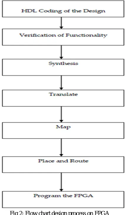
[image:3.612.205.419.237.601.2]For analysis Quartus2 software is used and for simulation Modelim is used, and for programming VHDL language is used. For analysis following steps are used .The very first step is VHDL coding to implement encoder and decoder based on FPGA programming which required to build a circuit is done in VHDL language. Another that is second step is simulation, Modelsim is used or simulation process, simulation s done to check working behavior and verification. Third step is synthesis using CAD tools by using Xillings. Which used to convert VHDL code into RTL schematic, next step is Translate and Map .Next one is place and route. Which translate code resources to FPGA resources .Place and route decide if interaction is establish if mapping is possible to FPGA .Then in next step generate programming file. And last one is download bit stream to FPGA.
Fig 2: Flow chart design process on FPGA
1) CRC Encoder And Decoder Circuit Design: In this section we are going to describe hardware design for CRC encoder and decoder .with error correction capability.
B. Abbreviations and Acronyms
Previous research is contained only serial and parallel implementation. which was depend n look up tables and division method of generator polynomial. But speed of algorithm was not too much high. To improve speed we used pipeline method which added more speed and accuracy. Also there were limits of error detection and correction capability of encoder which was updated up to 64 bits, but this algorithm is suitable for infinite number of bits.
Fig3: Output of CRC Decoder
Fig4: Logical view of encoder
C. Authors and Affiliations
T. V. Ramabadran and S. S. Gaitonde. [1] presented “A tutorial on CRC computations” presented in the paper. presented in the paper. The code has been verified for all possible lengths of message polynomial and generator polynomial calculation of remainder or redundant bits at the transmitter and checking the errors at the receiver is presented in the paper. The code has been verified for all possible lengths of message polynomial and generator polynomial. The CRC-4 to CRC-32 is successfully implemented.
Shukla S. nd Bergmann N. W.,[2] presented “Single bit error correction implementation in CRC-16 on FPGA . presented an efficient algorithm for parallel computation of the CRC in data transmission. Using CRC style checksums (cyclic redundancy check) is a simple and powerful method for detecting transmission error in data communication system. It is well suited for high speed serial transmission equipment, because it can be implemented on chip with a shift register and same XOR gates at nearly no cost. However, for some purposes it is necessary to implement a CRC calculation of the serial transmission chip, e.g., in additional error detection isrequired. The hardware implementation has been usedto improve the computation speed.
W.W.Peterson and D.T.Brown, G.Albertengo and R.Sisto, [3] presented “Parallel CRC Generation”. Parallel implementation is adopted which does not takes much time. CRC gives trade of between flexibility, performance and cost Generation for has been taken further than those enabled by tradition heterogeneous architectures based on microprocessor, DSP. CRC is very useful for error detection during data transmission. Having a look on the “CRC error detection method”, we can prefer that the method identifies the error correctly. Thus the „Parallel CRC generation and checking‟ is more efficient than the „Serial CRC generation‟, it
Castagnoli, G.: Brauer, s; Harrmnn,[4] presented a method “Optimization of cyclic Redundancy- check Codes with 24 and 32 parity Bits”. his brief lays out FPGA implementation of encoder and decoder for Golay codes. Golay codes are error detection and correction codes and it corrects errors in the receiving end in the received data to reduce retransmission events. Encoding algorithm for both the binary Golay code (G23) and extended binary Golay code (G24) implementation based on cyclic redundancy check encoding method. Decoding architecture for G24 (24, 12, 8) based on an error detection and correction method and here correction up to four errors is possible in the data .Synthesis and Simulation results obtained in Xilinx.
Sprachmann m [5] presented a technique of “Automatic generation of parallel CRC circuits,” Design and Test of Computers, which states that a Technique to model the error detection circuitry of CAN protocol in VHDL is described. The referred paper describes error circuitry in case of ‘no error’ our contribution – after reviewing the paper we designed error controlling circuitry for CAN bus in case of error.
III.CONCLUSION
The high speed design of CRC encoder and decoder algorithm implemented successfully time result without pipeline is shown in fig 5.Time result with pipeline for Xillings sparten 3E starter board is shown in Fig 6 , which proves that with pipeline algorithm become faster, which achieved high speed and greater throughput.
Fig5: Time analysis report without pipeline.
Fig6: Time analysis report with pipeline.
From above mentioned report throughput and frequency can be calculated. Frequency and throughput of both methods that is with pipeline and without pipeline are shown in below table.
A. Equations
1) To calculate Frequency F = 1/T (Where T= time)
2) Throughput= (Number of bits*maximum Frequency) ÷ Number of Clock Cycle
specification Without pipeline With pipeline
Time 15.34ns 5.48ns
Frequency 66Mhz 182Mhz
Power 0.081w 0.81w
Throughput (for 24 clock cycle)
22 Mbps 60.66Mbps
IV.ACKNOWLEDGMENT
It is our utmost duty and desire to express acknowledgement to the various torchbearers, who have rendered valuable guidance during the preparation of our project. First of all, we extend our deepest gratitude to our revered HOD. Dr. Mr. R.D. Ghongade
(HOD of electronics and Telecommunication Department)without whose support; our project could not have been transformed into
REFERENCES
[1] T. V. Ramabadran and S. S. Gaitonde. “A tutorial on CRC computations”. IEEE Micro, Vol. 8, No. 4, 1988, pp. 62-75.
[2] Shukla S. nd Bergmann N. W., “Single bit error correction implementation in CRC-16 on FPGA”1n: IEEE International conference on Field programmable technology. Brisbane ,Australia 2004
[3] W.W.Peterson and D.T.Brown, “Cyclic code for Error detection”,Proc.IRE,jan1961.[3]G.Albertengo and R.Sisto, “Parallel CRCGeneration”, IEEE Micro,Oct.1990 [4] R.Lee,, cyclic code Redundency,”Digital Design July 1977.
[5] A.Perez, “Byte-wise CRC Calculations”,IEEE Micro,June 1983. [6] A.S. Tanenbaum, “Computer Networks” , Prentice Hall,1981.
[7] T.V. Rambadran and S. S. Gaitonde, ’A Tutorial onCRC Computations’, IEEE Micro,Aug. 1988.
[8] K.V. GANESH, D. SRI HARI, and M. HEMA,” Design and synthesis of Field Programmable CRC Circuit Architecture”, International General of Engineering Research and applications, ISSSN22489622, volume1, Issue , Nov-dec2011.
[9] Programmable Gate Arrays, ACM press New York, NY, USA, 1999
[10] G.Campobello M. Russo, and G.Patane, “Parallel CRC Realization”,IEEE trans comput.,vol52,no10. [11] M.J.Smith , “Application specific Integrated Circuits”, Addision- Wesley Longman,jan1988
[12] C.Borrelli,”IEEE 802.3 Cyclic redundancy Check”, application note: virtex –II Family,XAPP209,Xilinx,Inc,March23,2001
[13] Castagnoli, G.: Brauer,s;Harrmnn,M.(june1993) “Optimization of cyclic Redundancy- check Codes with 24 and 32 parity Bits”. IEEE Transactions on communication 41(6):883.doi:10.1109/26.231911.