Abstract—This paper presents an analysis of a buck-boost converter with continuous input current that is useful for wide conversion range applications. Some of these applications include (i) power supply for portable devices where the battery is discharging, (ii) voltage regulated rectifiers with widely varying voltage, (iii) PV panels, in particular for obtaining the I-V curve, and (iv) burn-in test for power supplies.
This paper analyzes the CSC converter. This is the a dc-dc converter with only one switch and one inductor with that is able of of bucking or boosting the input voltage and providing a continuous input current. A detailed analysis along with simulation and experimental results are provided.
Index Terms— DC-DC power conversion, Power conversion, Pulse width modulated power converters, boost converter.
I. INTRODUCTION
OR voltage regulators in portable applications fed with a battery is highly desirable to work with a wide voltage range to optimize the battery charge. In some cases, it is also desirable to provide either a higher or a lower output voltage with respect to the voltage supply. For example to produce a fixed 3.3 V output as the battery voltage varies between 2.5 V and 5.5 V [1-5].
In other applications, for example a voltage-regulated rectifier with unity power factor (PFC) and uninterruptible power supply (UPS), one source is widely varying its voltage while the other is a constant dc battery or bus. Thus, a converter with buck and boost capability can be used for this purpose as well [10-18]. This feature can be performed by a traditional buck-boost converter. On the other hand, for minimizing EMI problems it is desirable for the converter to have continuous input current [6-9] which also optimizes the battery life. However, it is well-known that the traditional buck-boost converter has discontinuous input current.
Since a converter with buck and boost capability and continuous input current is highly desirable [8-9], the Cuk and SEPIC converters were developed. These converters can achieve those features with the draw-back of the use of an This work was developed under the project “Investigación de topologias de electronica de potencia” registered in DGEST 2011. J. C. Rosas-Caro, J. C. Mayo-Maldonado, J. E. Valdez-Resendiz, R. Salas-Cabrera, H. Cisneros-Villegas and R. Castillo-Ibarra are with the Madero City Technological Institute (e-mail [email protected]). J. G. Gonzalez-Hernandez is with Universidad Tecnologica de Altamira, Departamento de Mecatronica, Altamira, Mexico.
extra-inductor in comparison with traditional DC-DC converters topologies which use only one inductor. In addition, several solutions such as cascading converters have been employed [3-5].
An emerging but also important application for converters with buck-boost capability is the measuring of the the I-V curve of PV panels [16] for this purpose, the continuous input current is required along with the capability of bucking and boosting the input voltage.
After a deep review of the topological literature [6, 8-9, 16-24], only one topology with buck-boost voltage capability and continuous input current that employs only the basic components such as one voltage source, one inductor, one capacitor, one transistor and one diode (two transistor and diodes if bidirectional power flow is required) was found. However, it has been apparently hidden in literature for more than 20 years [25] even in modern literature where the topology appears [18]. In other words, their benefits, applications, design-oriented analysis and modeling have not been fully explored and reported.
The purpose of this paper is to analyze and model this converter that is called CSC converter. This converter has the advantage of providing a continuous input current and a simple structure which has the basic components of the traditional buck-boost converter components. A detailed analysis along with simulation and experimental results are provided.
I. THE CSC CONVERTER
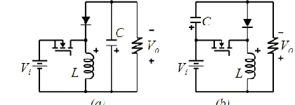
The CSC converter is shown in Fig. 1 along with the traditional buck-boost converter. As mentioned before, after a deep review of the literature authors has found the topology in Fig. 1(b) in [25], [18]. However a deep analysis of this converter is still missing. In this paper, some of the features such as waveforms, modeling and design analysis for this converter are explored.
Fig. 1. (a) Traditional buck-boost converter, (b) CSC converter.
Design-Oriented Analysis and Modeling of a
Single-Inductor Continuous Input-Current
Buck-Boost DC-DC Converter
J. C. Rosas-Caro, J. C. Mayo-Maldonado, J. E. Valdez-Resendiz, R. Salas-Cabrera,
H. Cisneros-Villegas, R. Castillo-Ibarra, J. G. Gonzalez-Hernandez
[image:1.612.328.538.644.719.2]As seen in Fig. 1, the CSC topology is similar to the traditional buck-boost converter, the topological difference is the capacitor’s connection which is connected from the diode to the positive side of input voltage instead of been connected from the diode to the negative side if the input voltage.
A. Steady state operation in CCM
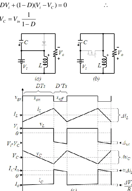
Fig. 2 shows the equivalent circuit according with the switching state, and some important waveforms in continuous conduction mode CCM.
Defining d as the duty cycle, the time when the switch is on over the total switching period Ts and by using the small ripple approximation [6], the average voltage across the inductor in steady state can be expressed as:
)
)(
1
(
)
(
i i CL
t
DV
D
V
V
v
(1)Note than the DC-component of variables d, vC and vi are written as D, and VC and Vi respectively, during the steady state, this average voltage as the average current in the capacitor are equal zero, and then the voltage in the capacitor can be expressed as:
0
)
)(
1
(
i Ci
D
V
V
DV
D
V
V
C in
1
1
(2)Fig. 2. Equivalent circuits for the switching states in CCM when (a) the switch is on (b) the switch is off (c) some important waveforms.
[image:2.612.323.557.213.274.2]The voltage in the capacitor is the same as in a traditional boost converter, but in this case the output voltage is not given only by the capacitors voltage but also by the input voltage, because the input voltage is in series with the capacitor voltage, and then, considering the polarity signs defined in
Fig. 1 and Fig. 2, the output voltage can be expressed as:
D
D
V
V
D
V
V
V
V
o C i i i i
1
1
1
(3)The CSC converter has the same conversion ratio than the traditional buck-boost converter. The main advantage of the proposed converter can be seen in Fig. 1 and Fig. 2, the input voltage is connected to the reference node with the inductor and the load, both the inductor and the load drain a continuous current and then the input voltage becomes continuous.
Now lets to derive the DC-current in the inductor. By using the small ripple approximation, the average current in the capacitor can be expressed as:
R
V
V
I
D
R
V
V
D
t
i
C iL i
C
C
(
)
(
1
)
L i
C
C
D
I
R
V
V
t
i
(
)
(
1
)
(4) During the steady state, this average current is equal zero, and then the current in the inductor can be expressed as:R
D
V
V
I
C iL
)
1
(
(5)By substituting (2) in (5) the DC-current in the inductor is expressed as:
1
1
1
)
1
(
1
1
)
1
(
1
D
R
D
V
V
D
V
R
D
I
ii i
L
2
)
1
(
D
D
R
V
I
iL
(6) The switch and diode voltage and current stress can be calculated with a similar procedure.When the switch is open it blocks the capacitors voltage given by (2) this is actually the same voltage rating for a switch in a traditional buck-boost converter and in the Cuk converter, the current in the switch can be averaged from the switching states (Fig. 2) and expressed as:
2
1
)
(
D
D
R
V
DI
t
i
iL
S (7)
As the inductor current in the input-series buck-boost converter is the same as in the traditional buck-boost converter for converters rated to the same voltage and output power, the current in the switch is the same and we can say the switch is identical in the proposed topology than in the traditional buck-boost converter.
When the diode is open it blocks the voltage in the capacitor expressed in (2) and the same as in the traditional buck-boost converter, the average current can be expressed as:
D
D
R
V
D
D
R
V
D
I
D
t
i
i iL
D
1
)
1
(
)
1
(
)
1
(
)
(
2 [image:2.612.59.274.336.647.2]This is also the same as in the traditional buck-boost converter. The steady state analysis is then resumed in equations (2), (3), (6), (7) and (8), it can be seen the proposed converter has the same inductor, transistor and diode than the traditional buck-boost converter.
From those equations, the main disadvantage of the proposed topology can be seen; the capacitor has the same voltage as the traditional boost converter, which is higher than in the traditional buck-boost converter, so far in the authors understanding this is the only disadvantage of the discussed topology, this disadvantage is also presented in one of the capacitors of the Cuk and in the SEPIC converter which are the other buck-boost converters with continuous input current.
II. DESIGN ORIENTED ANALYSIS
For selecting the inductance and capacitance, the equations for the voltage-ripple in the capacitor and current ripple in the inductor can be derived by using the small ripple approximation [6]. From Fig. 2, the inductor current can be expressed during the time when the switch is on as:
S i
L
V
DT
L
i
1
(9)The input current Ii is the sum of the inductor current IL plus the load current Io, the output current is decreasing during the on-time when the input current is increasing because the capacitor is discharging during this time, that means the output current ripple ΔIo cancels part of the inductor current ripple ΔIL and then the input current ripple ΔIi is smaller than the inductor current ripple ΔIL, but since the load current ripple is expected to be pretty small by selecting a correct capacitor value, the load current ripple may be neglected for calculating the input current ripple and the input current ripple can be approximated to the inductor current ripple.
During the same time (when the switch is off) the capacitor voltage ripple (see Fig. 2) can be expressed as:
S o
C
I
DT
C
v
1
(10)Similar to the input current-tipple, neglecting an input voltage ripple, the output voltage ripple is the same as the capacitors voltage ripple.
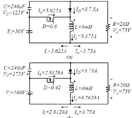
A. Design example
A CSC converter will be feed with a voltage between 50V
to 100V it is desired to have a constant output voltage of 75V, the load is a 20Ω resistor, the desired input current ripple is 20% of the input current (which ensures operation in CCM) and the output voltage ripple 1% of the rated output voltage, the switching frequency is 25 kHz.
Note: since the oversize-percentage of all components is up to the designer, the components variables will be provided from the described equations (without oversize), security considerations for operating the converter under different conditions and losses won’t be considered in this design example. The solution is shown in Fig. 3.
Since the input voltage may vary from 50V-to-100V the converters gain would vary from 1.5-to-0.75 and the duty cycle D will vary from 0.6-to-0.42. Two extreme operating points will be defined, A is when the input voltage is 50V, and
[image:3.612.322.553.111.319.2]B is when the input voltage is 100V, see Fig. 3.
Fig. 3. Design example with both extreme operation points.
B. Capacitor selection
The minimum voltage stress would be when the input is 50V; the capacitor would have 125V DC according with (2), the maximum one would be when the input is 100V and the capacitor would have 175V DC. The maximum output voltage ripple needs to be 0.75V (1% of 75V), from (10) it can be seen that the ripple will vary with the duty cycle, and the maximum would be when the duty cycle is the higher (0.6) and then:
40
6
.
0
5
.
7
1
75
.
0
1
C
DT
I
C
v
C o S (11)And from (11) and the above explanation, a capacitor of 240μF is selected with a voltage rating of 175V.
C. Inductor selection
The minimum current stress would be when the input is 100V; according with (6) the inductor-current would be 6.5628A in point B (100V input), the maximum inductor current would be 9.375A in point A. The input current ripple is the same as the inductor current ripple which is given by (9). In point B the input current is higher and then the input current would be set to 20% of 2.8128A.
40
42
.
0
100
1
5625
.
0
1
L
DT
V
L
i
L i S (12)And from (12) and the above explanation, an inductor of 3mH is selected with a current rating of 9.57A (9.37A + 200mA), this is because according with (6) the current ripple in point A is equal to (13):
mA
m
i
L50
0
.
6
40
400
3
1
And the maximum current in the inductor would be the DC current in point A plus a half of its current-ripple at that point.
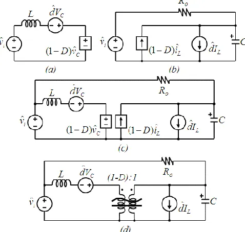
III. SMALL SIGNAL MODELING AND EQUIVALENT CIRCUITS
This section presents the small signal model along their equivalent circuit models. First of all the average dynamic equations should be writhen from the equivalent circuits according with the switching state. From Fig. 2 the state equation for the inductor can be written as:
C i
L
v
d
v
dt
i
d
L
(
1
)
(14) All variables are writhen in lower case for indicated they are not constant. In an analog way, the state equation for the capacitor can be written as (15).R
v
v
i
d
dt
dv
C
C iL
C
(
1
)
(15)The next step is to consider that all variables: the duty cycle
d, the input voltage vi, the capacitor voltage vC and the inductor current iL are composed by a large constant value plus a small ac component:
C C
C
V
v
v
ˆ
; iL ILiˆLd
D
d
ˆ
:v
i
V
i
v
ˆ
i (16) By substituting (16) in (14) one gets:
I
Li
L
V
iv
i
D
d
V
Cv
C
dt
d
L
ˆ
ˆ
1
ˆ
ˆ
C C i i L
L
V
v
V
v
dt
i
d
L
dt
dI
L
ˆ
ˆ
ˆ
C C C
C
D
v
d
V
d
v
DV
ˆ
ˆ
ˆ
ˆ
(17)From (17) the derivative of IL is zero since that is the dc component of the inductance current, and since Vi is equal to
(1-D)VC the constant components of (17) cancel each other, and then (17) becomes:
C C C i
L
v
D
v
d
V
d
v
dt
i
d
L
ˆ
ˆ
(
1
)
ˆ
ˆ
ˆ
ˆ
(18) The linearization of small signal modeling is based on considering the multiplication of ac components is negligible small since they are small signals and the product of two small signal is a signal too small, and then from (18) the small signal equation becomes:C C i
L
v
D
v
d
V
dt
i
d
L
ˆ
ˆ
(
1
)
ˆ
ˆ
(19) This may be represented by a circuit model, see Fig. 4(a). In the other hand, by substituting (16) in (15) and following the same procedure one gets:L L L L L L C
C
I
i
DI
D
i
d
I
d
i
dt
v
d
C
dt
dV
C
ˆ
ˆ
ˆ
ˆ
ˆ
ˆ
R
v
R
V
R
v
R
V
C
ˆ
C
i
ˆ
i
(20)From (20) the derivative of VC is zero since that is the dc component, from (5), the constant components in (20) cancel each other; and then (20) becomes:
L i C L L
C
d
i
R
v
v
I
d
i
D
dt
v
d
C
ˆ
(
1
)
ˆ
ˆ
ˆ
ˆ
ˆ
ˆ
(21) By neglecting the multiplication of two ac signals, as explained because of the small signal linearization (21) becomes:R
v
v
I
d
i
D
dt
v
d
C
C iL L
C
(
1
)
ˆ
ˆ
ˆ
ˆ
ˆ
(22)This may be represented by a circuit model, see Fig. 4(b). Both circuit model combined are shown in Fig. 4(c) and a full circuit model with an ideal transformer is shown in Fig. 4(d).
Fig. 4. Small signal ac circuit models (a) equivalent to equation (19) (b) equivalent to equation (27) (c) equivalent circuit model (d) equivalent circuit model with the ideal transformer.
IV. DISCONTINUOUS CONDUCTION MODE
The CSC converter can be designed with parameters to ensure the current in the inductor is continuous as in the design example, but it can be designed for operate in discontinuous conduction mode.
The current ripple during the time interval DTS is still expressed as (9), the current in the inductor would be continuous if the DC component (6) is higher than a half of the current ripple expressed in (9) and then:
S i L
i
L
V
DT
L
i
D
D
R
V
I
2
1
2
)
1
(
2
[image:4.612.320.559.312.539.2]From (28) it can be seen that: 2
)
1
(
2
D
RT
L
S
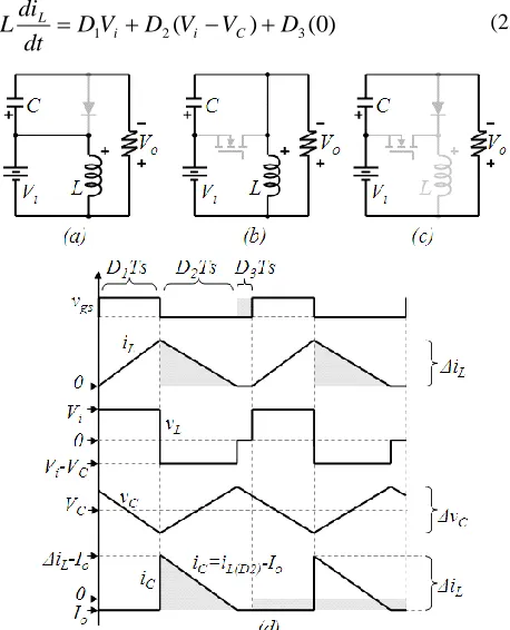
(24)Equation (24) express the relation between constant parameters and the duty cycle which may change during the operation, traditionally 2L/RTS is defined as K and the function of D as a KCRIT the converter would operate in continuous conduction mode CCM if K>KCRIT. Otherwise the converter operates in DCM. This condition is the same for the traditional buck-boost converter. For calculating the boost-factor during the DCM equations for the volts-per-second for the inductor and amps-per-second in the capacitor should be analyzed, since the output capacitor should be calculated to maintain a constant voltage, the small ripple approach can be considered for the capacitor voltage but not for the inductor current which would seems such as shown in Fig. 5. In the DCM there are three switching states, instead of two, an extra switching state is when both diode and transistors are open, remember the diode is closed by inductor current when the switch is off, and then when the inductor current reaches zero, the diode opens, before the switch closes, the equivalent circuits and important waveforms are shown in Fig. 5, instead of dividing the switching period in two time-periods this would be divided into three time periods, D1TS, D2TS and D3TS, see Fig. 5, the inductor voltage can be expressed as:
)
0
(
)
(
32
1
V
D
V
V
D
D
dt
di
L
i i CL
(25)Fig. 5. Equivalent circuits for the switching states in CCM when (a) the switch is on and the diode is off (b) the switch is off and the diode is on (c) both diode and switch are off (d) important waveforms.
In steady state this voltage along with the capacitor current should be zero and then:
2(
)
3(
0
)
0
1
V
D
V
V
D
D
i i Ci C
i
V
V
V
D
D
12 (26)
From Fig. 5 the capacitor is discharge by the load current while is charged with the inductor current during D2, see gray areas in the capacitors current in Fig. 5, in steady state, the sum of both should be zero, the amps-per-second that charges the capacitor can be calculated as the area of iL during D2 shown in gray color in Fig. 5, and this should be equal to the load current which discharges the capacitor all the time:
R
V
V
i
D
C iL
2
2
1
(27)The current ripple is still expressed as (9) and then:
R
V
V
T
D
V
L
D
C iS
i 1
2
1
2
1
i C
i
D
D
V
V
V
K
1 2
1
(28) Where K=2L/RTS, by substituting (26) in (28):
C ii C
i
i
V
V
V
V
V
D
D
V
K
1 11
1
11
1
K
D
V
V
D
V
K
V
C i i i (29)And then, the output voltage can be derived as (30):
C i i i io
V
D
V
V
K
V
V
V
1
1K
D
V
V
i
o
1 (30)This is the same gain as the traditional buck-boost converter in DCM. And By substituting (29) in (26) the time-period D2 can be expressed as:
1 1
1 1
2
1
1
D
V
K
V
D
V
V
D
V
K
V
D
D
i i
i i i
i
K
V
D
V
D
K
D
i
i
1 1
2 (31)
V. EXPERIMENTAL RESULTS
[image:5.612.59.288.381.664.2]VI. CONCLUSION
This paper discusses an outstanding buck-boost dc-dc converter topology with the advantage of providing a continuous input current and a simple structure; it has the basic components of the traditional buck-boost converter.
The CSC converter may be used for voltage regulation in portable devices where the battery is discharging and the voltage regulator need to work with a wide voltage range. Another possible application are voltage-regulated rectifiers with unity power factor PFC and uninterruptible power supply UPS where one of the source, or load, is a widely varying voltage while the other is a constant dc battery or bus. And finally an emerging application for converter with buck-boost capability is the measuring the I-V curve of PV panels where the continuous input current along with the capability of bucking and boosting the input voltage is required. More information will be published in future work for space reasons.
[image:6.612.48.282.299.562.2]A detailed analysis along with simulation and experimental results are provided.
Fig. 6. Experimental prototype.
Fig. 7. Experimental results of the input current and the output voltage.
REFERENCES
[1] Ping-Ching Huang; Wei-Quan Wu; Hsin-Hsin Ho; Ke-Horng Chen; , "Hybrid Buck–Boost Feedforward and Reduced Average Inductor Current Techniques in Fast Line Transient and High-Efficiency Buck– Boost Converter," Power Electronics, IEEE Transactions on , vol.25, no.3, pp.719-730, March 2010.
[2] Wan-Rone Liou; Mei-Ling Yeh; Yueh Lung Kuo; , "A High Efficiency Dual-Mode Buck Converter IC For Portable Applications," Power Electronics, IEEE Transactions on , vol.23, no.2, pp.667-677, March 2008.
[3] Datasheet for LTC3440, Micropower Synchronous Buck-Boost DC/DC Converter. [Online]: Available. www.linear.com.
[4] Midya, P.; Haddad, K.; Miller, M.; , "Buck or boost tracking power converter," Power Electronics Letters, IEEE , vol.2, no.4, pp. 131- 134, Dec. 2004.
[5] Sahu, B.; Rincon-Mora, G.A.; , "A low voltage, dynamic, noninverting, synchronous buck-boost converter for portable applications," Power Electronics, IEEE Transactions on , vol.19, no.2, pp. 443- 452, March 2004.
[6] Erickson R., Maksimovic D., Fundamentals of Power Electronics. Second Edition, USA: Kluwer Academic Publishers, 2001.
[7] M. A. Al-Saffar, E. H. Ismail, A. J. Sabzali, and A. A. Fardoun, “An improved topology of SEPIC converter with reduced output voltage ripple,” IEEE Trans. Power Electron., vol. 23, no. 5, pp. 2377–2386, Sep. 2008.
[8] Cuk, Slobodan; Middlebrook, R. D.; , "Advances in Switched-Mode Power Conversion Part I," Industrial Electronics, IEEE Transactions on , vol.IE-30, no.1, pp.10-19, Feb. 1983.
[9] Cuk, Slobodan; Middlebrook, R. D.; , "Advances in Switched-Mode Power Conversion Part II," Industrial Electronics, IEEE Transactions on , vol.IE-30, no.1, pp.19-29, Feb. 1983.
[10] Pires, V.F.; Silva, J.F.A.; , "Single-stage three-phase buck-boost type AC-DC converter with high power factor," Power Electronics, IEEE Transactions on , vol.16, no.6, pp.784-793, Nov 2001.
[11] Vitor Fernao Pires; Silva, J.F.; , "Three-phase single-stage four-switch PFC buck-boost-type rectifier," Industrial Electronics, IEEE Transactions on , vol.52, no.2, pp. 444- 453, April 2005.
[12] Andersen, G.K.; Blaabjerg, F.; , "Current programmed control of a single-phase two-switch buck-boost power factor correction circuit," Industrial Electronics, IEEE Transactions on , vol.53, no.1, pp. 263- 271, Feb. 2006.
[13] Ismail, E.H.; Sabzali, A.J.; Al-Saffar, M.A.; , "Buck–Boost-Type Unity Power Factor Rectifier With Extended Voltage Conversion Ratio," Industrial Electronics, IEEE Transactions on , vol.55, no.3, pp.1123-1132, March 2008.
[14] Jingquan Chen; Maksimovic, D.; Erickson, R.W.; , "Analysis and design of a low-stress buck-boost converter in universal-input PFC applications," Power Electronics, IEEE Transactions on , vol.21, no.2, pp. 320- 329, March 2006.
[15] Kamnarn, U.; Chunkag, V.; , "Analysis and Design of a Modular Three-Phase AC-to-DC Converter Using CUK Rectifier Module With Nearly Unity Power Factor and Fast Dynamic Response," Power Electronics, IEEE Transactions on , vol.24, no.8, pp.2000-2012, Aug. 2009.
[16]Aranda, E.D.; Galan, J.A.G.; de Cardona, M.S.; Marquez, J.M.A.; , "Measuring the I-V curve of PV generators," Industrial Electronics Magazine, IEEE , vol.3, no.3, pp.4-14, Sept. 2009.
[17] D. W. Hart, Introduction to Power Electronics. Englewood Cliffs, NJ: Prentice-Hall, 1994.
[18] Williams, B.W.; "Basic DC-to-DC Converters," Power Electronics, IEEE Transactions on, vol.23, no.1, pp.387-401, Jan. 2008.
[19] Makowski, M.S.; , "On topological assumptions on PWM converters-A reexamination," Power Electronics Specialists Conference, 1993. PESC '93 Record., 24th Annual IEEE , vol., no., pp.141-147, 20-24 Jun 1993. [20] Hopkins, D.C.; Root, D.W., Jr.; , "Synthesis of a new class of converters
that utilize energy recirculation," Power Electronics Specialists Conference, PESC '94 Record., 25th Annual IEEE , vol., no., pp.1167-1172 vol.2, 20-25 Jun 1994.
[21] Peng, F.Z.; Tolbert, L.M.; Khan, F.; , "Power electronics' circuit topology - the basic switching cells," Power Electronics Education, 2005. IEEE Workshop , vol., no., pp. 52- 57, June 16-17, 2005
[22] Khan, F.H.; Tolbert, L.M.; Peng, F.Z.; , "Deriving New Topologies of DC-DC Converters Featuring Basic Switching Cells," Computers in Power Electronics, 2006. COMPEL '06. IEEE Workshops on , vol., no., pp.328-332, 16-19 July 2006.
[23] Ke Zou; Scott, M.J.; Jin Wang; , "The analysis of DC-DC converter topologies based on stackable voltage elements," Energy Conversion Congress and Exposition (ECCE), 2010 IEEE , vol., no., pp.4428-4433, 12-16 Sept. 2010.
[24] Tymerski, R.; Vorperian, V.; , "Generation and classification of PWM DC-to-DC converters," Aerospace and Electronic Systems, IEEE Transactions on , vol.24, no.6, pp.743-754, Nov 1988.
[25] Hua, G.-C.; Huang, S.-P.; , "New PWM switched-mode converter topologies," Power Electronics Specialists Conference, 1988. PESC '88 Record., 19th Annual IEEE , vol., no., pp.150-156 vol.1, 11-14 April 1988.