quantum well structures
John P. Doran Fred P. Logue T. Miyajima* Ross P. Stanleyt John F. Donegan John Hegarty Trinity College Department of Physics Dublin 2, Ireland
E-mail: [email protected]
Abstract. The excitonic transition in Il-VI quantum well materials has recently been used as the basis for optical modulators and also as the lasing transition at low temperatures. The central aspect in the use of the exciton resonance in optical devices is the understanding of the ex-citon linewidth. We present a detailed study of the interactions that affect the linewidth in Il-VI semiconductor quantum well materials. The broad-ening of the resonance with increasing temperature can be controlled by altering the material parameters of the Il-VI structures. In so doing the exciton binding energy can exceed the LO-phonon energy and thereby reduce the homogeneous contribution to the measured linewidth. Efforts to reduce well-width fluctuations in the growth of the Il-VI quantum well structures, which are responsible for the inhomogeneous linewidth, must also be made to a limit where the room temperature Iinewidth is narrow and homogeneously broadened.
Subject terms: II- VI semiconductors; quantum wells; excitons; photoluminescence; linewidth.
Optical Engineering 33(12), 3921—3925 (December 1994).
1 Introduction
Forseveral decades, excitons have been studied in bulk semi-conductor materials. These studies were concerned primarily with the elucidation of exciton dynamics in semiconductors at low temperatures.' The parallel development of electronic semiconductor devices operating at room temperature was little influenced by this study of exciton dynamics. This is due to the fact that the exciton, which is a weakly bound electron-hole pair, is ionized at room temperature and there-fore does not contribute to the electronic properties at room temperature. The advent of molecular beam epitaxy and other thin-film growth techniques means that we can now produce a layer of one semiconducting material with a small bandgap between two layers with high bandgap. Because the layers we can produce are of the size of the exciton Bohr radius, we expect and find in experiments that we have produced real quantum well systems familiar from elementary quantum mechanics. Excitons are observed in these systems at room temperature, and optoelectronic devices based on exciton dynamics have been developed. For the present generation of devices, we have the potential to control exciton dynamics through changes in material composition. A detailed
under-*Cunent address: Sony Corporation Research Center, 174 Fujitsuka-cho, Hodogaya-ku, Yokohama 240, Japan.
tCurrent address: IMO, Department de Physique, Ecole Polytechnique Federale, CH-1015 Lausanne, Switzerland.
Paper 01-022 received June 20, 1994; accepted for publication Aug. 22, 1994. 1994 Society of Photo-Optical Instrumentation Engineers. 009 l-3286/94/$6.00.
standing of exciton dynamics in quantum-confined systems is therefore essential so we can provide an engineering-type approach for future device applications. In this paper we look in detail at one aspect of exciton dynamics, the exciton line-width, and at the interactions that alter the linewidth and our ability to control the linewidth for excitonic applications.
2 Excitons and Quantum Confining Systems Anexciton is an electron-hole pair bound through their mu-tual Coulomb interaction. In analogy with the hydrogen atom the exciton binding energy in a bulk material is given by:
2m e4
Eb=h2(8r)2
, (1)where m,. 5 the reduced mass of the exciton and is the dielectric constant. The exciton binding energy is dependent on the semiconductor material. If we perform an absorption experiment on a semiconductor material, we expect to find the threshold for absorption at the bandgap energy Eg.Infact,
we find for high-quality material such as GaAs, a hydrogenic series of levels below the bandgap corresponding to the ex-citon series.2 The iS exex-citon state occurs at energy Eg Eb.
These lines are sharp as opposed to the broad absorption bands observed above Eg.
or 2-D binding energy is four times greater than the bulk or 3-Dcase.3In forming real quantum well materials, we wish to choose structures such that the binding energy is substan-tially enhanced over the bulk case so that we can use them in optoelectronic devices at room temperature.
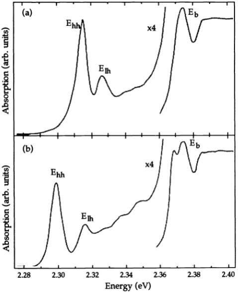
By extension of the bulk case, the absorption spectrum of a quantum confined structure will consist of a fundamental bandgap energy Egabovewhich band absorption occurs and below which we find the hydrogenic exciton series. As a result of the greater exciton binding energy in the confined system, the exciton peak will be shifted by a greater extent from the bandgap than in the bulk material. We show the low-temperature absorption of CdZnTe/ZnTe quantum well materials in Fig. 1 as an illustration. The lowest exciton fea-ture is split into two due to the different masses associated with the light and heavy holes in the valence band.
At 10 K the excitonic features in Fig. 1 have a linewidth of about 5 meV, which broadens with temperature. To op-timize these devices, we need to know the mechanisms behind the broadening of the exciton feature and from there to sug-gest ways to control the broadening.
3
A Simple Electro-Optic DeviceIf
we apply an electric field to a semiconductor sample, we effectively reduce its bandgap and therefore the exciton res-onance moves to lower energy.4 If light of energy Ekcor-Fig. 1 Absorption spectrum for CdZnTe/ZnTe multiple quantum well
samples with well widths of 50 and iooA. The main absorption
peaks at low energy are due to heavy-hole and light-hole exciton
transitions, and Eb corresponds to the energy gap of the ZnTe buffer
layer in the sample.
responding to the peak of the exciton resonance is shone onto a sample, the light is strongly absorbed. To make an effective modulator, we need to have as large an on/off ratio for the device as possible. In our case this corresponds to a large change in the absorption oflight in the quantum well sample. We can achieve this by applying an electric field to the sample shifting the exciton peak to lower energy. This phenomenon is known as the quantum-confined-Stark effect.5 Light of energy EPk 5 no longer strongly absorbed by the sample. Ideally, we could change from a large absorption feature to zero absorption, giving a large modulation depth for the device.
For real quantum well samples, we find that the exciton resonance broadens as well as shifts when we apply an electric field. The application of an electric field has the effect of polarizing the exciton. The barrier walls prevent the disso-ciation of the exciton and thereby allow us to observe ex-citonic features to much higher electric field strengths in quantum well compared with bulk systems. The exciton fea-ture is broadened due to the well-width fluctuations that occur during the growth process and that alter the ''local'
'
potentialwell ofthe exciton. Our goal therefore is to produce an exciton feature with a very small linewidth so that the application of an electric field shifts the resonance sufficiently to make a good modulator but does not appreciably broaden the exciton resonance. We therefore need to know the factors that govern the linewidth of the exciton resonance in quantum well systems.
4
The Exciton LinewidthAswith all experimentally measured optical linewidths, the measured exciton linewidth Fm is composed of an inhomo-geneous F and a homoinhomo-geneous part h' which when con-voluted together give the measured linewidth We con-sider the two parts separately.
4.1 Inhomogeneous Broadening
Theinhomogeneous broadening of the exciton linewidth oc-curs due to variations in the sample parameters. For quantum well materials this is normally due to well-width fluctuations between the well and barrier materials. The exciton res-onance is sensitive to the ''local'' wellwidth and therefore the exciton acquires a width LE due to these fluctuations. Well-width fluctuations arise during the growth process and tremendous efforts have been made to reduce the inhomo-geneous broadening in quantum well systems. For presently available high-quality Ill-V GaAs-based quantum well sys-tems, linewidths of the order of 0.5 meV at low temperatures are now commonly available.6 We are now approaching the
linewidth of exciton features observed in bulk
semi-conductors, which is probably a realistic limit for future quan-tum well materials. For materials with an alloy well material, there is an additional broadening of the exciton due to po-tential fluctuations occurring due to the random ordering of atoms in the lattice.
4.2 Homogeneous Broadening
Thetwo contributions to the homogeneous linewidth are (1) broadening due to the finite lifetime of the excitons and (2) broadening due to scattering events in the semiconductor material. In the limit of low exciton densities the main scat-2.34
[image:2.618.62.302.383.677.2]tering events are due to the exciton-phonon interaction, known as the FrOhlich interaction. Because the population of phonons is temperature dependent, we expect that the homogeneous contribution to the broadening is also tem-perature dependent. Acoustic and optic phonons both partic-ipate in these interactions. The interaction with the high-energy LO phonons is by far the strongest scattering event for excitons. This is due to the distortion of the unit cell, which produces an electric field with which the exciton can interact. The homogeneous exciton-linewidth is given by7:
F,, FPh/[exp(hv/kT) —
1
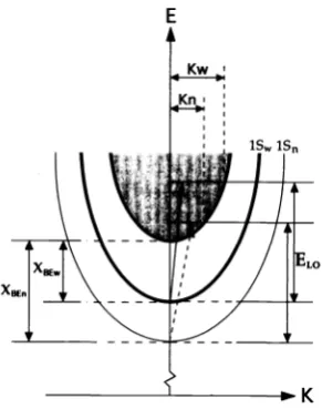
, (2)where hv is the LO-phonon energy and ph 5 the phonon interaction parameter and describes the strength of the exciton-phonon interaction. Our aim is to reduce 'Ph by en-gineering the quantum well structure; 'Ph is determined by the Fröhlich interaction and the number of final states into which the exciton can be scattered. The Fröhlich interaction is basically determined by the material, be it GaAs or ZnSe, but not by quantum confinement in these materials. On the other hand, the number of final states for scattering can be altered by adjusting the quantum well material. This is most easily achieved by varying the well width in the structure. In Fig. 2 we show the exciton dispersion curve for a narrow (n) and a wide (w) well. Also indicated are the corresponding
exciton binding energies XBEfl and XBEW and the LO-phonon
energy ELO. When the exciton binding energy XBE is smaller than ELO, the zone center excitons can be scattered into the continuum states as well as exciton bound states away from the zone center. As the exciton binding increases, the range of wave vector states available decreases (range of K less than range of K in Fig. 2). If XBE exceeds ELO, scattering to continuum states is no longer possible. This process should lead to a strong reduction in broadening with temperature and therefore to a smaller observed linewidth at room tem-perature.
For Ill-V materials such as GaAs, XBE is about 8 meV and ELO 5 about 36 meV. On the other hand, IT-VT materials have a much greater XBE; for ZnSe, XBE is 20 meV, whereas for ELO it is 30 meV. Quantum confining excitons in Il-VT structures should allow us to fulfill the condition XBE>ELO and thereby reduce Ph Evidence to support this framework has been found for the CdZnSe/ZnSe and CdZnTe/ZnTe
sys-tems.8'9
To provide a method to control the exciton linewidth, we need to do the following:
1 . Measurethe linewidth as a function of temperature for a series of samples with varying well widths.
2. Determine the inhomogeneous contribution F1 to the linewidth.
3. Deconvolute the inhomogeneous contribution. 4. Fit the resulting homogeneous contribution Fhto Eq. (1)
in order to determine FPh.
5. Define the material parameters for which and F1 are simultaneously minimized.
5
The Measured Exciton LinewidthThe inhomogeneous contribution to the measured exciton linewidth is due to the material fluctuations that have a
100 150 200 250
Temperature(K)
Fig.3 Filled circles are the measured linewidth Fm for the 70-A CnZnTe/ZnTe quantum well; open circles are the values of the ho-mogeneous linewidth h obtained by numerical deconvolution of the inhomogeneous linewidth F1. The solid line is a fit to Eq. (2) with
Ph 17.0 meV. The dashed line gives "ph 9 meV. The inset shows the dependence of ph on the well width.
Gaussian-shapeddistribution. The exciton scattering and re-combination events are responsible for the homogeneous con-tribution to the measured linewidth and have a Lorentzian-shaped distribution. The measured linewidth will contain both homogeneous and inhomogeneous contributions and the measured linewidth will be a convolution of a Lorentzian and a Gaussian distribution, known as a Voigt distribution. In Fig. 3 we show the results of our studies of the exciton linewidth in a 70-A CdZnTe/ZnTe single quantum well sam-ple. We note the following results:
[image:3.615.360.506.55.240.2]1. The low-temperature lineshape is a Gaussian and the measured low-temperature linewidth is taken to be the inhomogeneous linewidth F,. At low temperatures (10
Fig. 2 Schematic diagram showing the effect of increased exciton binding energy XBE in a narrow well. The range of continuum wave vector states available in the narrow well, K,,, is smaller than in the
wide well, K.
10
8
Eo
4
0 0
[image:3.615.319.563.325.480.2]K) the phonon population is negligible and so only the lifetime contributes to the homogeneous linewidth. For CdZnTe/ZnTe quantum wells,'° the lifetime is about 100 ps at 10K corresponding to a linewidth of45 kieV. The measured 10—K linewidth is about 3 to 4 meV for these materials and so we are dominated by the in-homogeneous linewidth at low temperature.
2. As the temperature is raised the exciton linewidth in-creases and concomitantly the lineshape gradually changes from a Gaussian to a Voigt. The inhomoge-neous linewidth F1 is independent of temperature, whereas the homogeneous contribution depends on the phonon population and is strongly temperature dependent.
3. To determine the homogeneous linewidth F,,, we must deconvolve the inhomogeneous contribution I's. To ob-tam the true 'h' we must numerically deconvolve F, from the measured Fm.
In the literature we find that the inhomogeneous lineshape is approximated as a Lorentzian, then because the homoge-neous contribution is also a Lorentzian, the deconvolution is achieved simply by subtracting the two linewidths. This has been used extensively in the literature on GaAs materials.' In Fig. 3 we show the results of our numerical deconvolution
and that produced using the approximation oftwo Lorentzian lines for the 70-A CdZnTe sample. We see immediately that
FPh much smaller using the approximation method. To
compare different materials where the inhomogeneous and homogeneous contributions can be widely different, the nu-merical procedure described earlier must be used. A detailed analysis of the deconvolution procedure will be published elsewhere.'2 For our present purposes, we wish to point out the need for proper deconvolution so that meaningful com-parisons between materials can be made.
The inset in Fig. 3 shows the variation of FPh for three CdZnTe/ZnTe wells. We see that FPh is smallest for the 40-A well in accordance with the model given earlier. For this well the exciton binding energy is approximately equal to the LO-phonon energy with the result that the scattering is strongly reduced.9 This characteristic is unique to Il-VI semi-conductors and has also been observed in the CdZnSe/ZnSe systems.8 For 111-V materials the opposite trend is observed, i.e., the broadening is strongest in the narrower wells. This is due to the much greater LO-phonon energy in these ma-terials with the result that the inequality XBE>ELO cannot be achieved.
6
Materials Engineering of the Exciton LinewidthToachieve our goal of minimum exciton linewidth at low temperature, we need to reduce simultaneously the inhom-ogeneous and hominhom-ogeneous contributions to the observed linewidth. For Il-VI materials, with which we are chiefly concerned here, we need to use nanow quantum well samples to achieve as small a broadening factor FPh as possible. How-ever, as the wells are narrowed the inhomogeneous contri-bution increases. This is due to the stronger interaction with the well-width fluctuations, which are an inevitable part of the growth procedure. Therefore, there is a trade-off between
what we can achieve with decreasing FPh and therefore Fh and increasing F due to the well-width fluctuations. Our approach must then be as follows:
1. We must define the material parameters for which XBE>ELO for each Il-VI system studied. The value of
XBEdependsprincipally on well width and confinement
energy and so a range for both these quantities needs to be specified. Note also that, for very narrow wells, the exciton wave function penetrates strongly into the barrier with a concomitant reduction in the exciton binding energy. A recent study'3 of the newly devel-oped ZnSe/ZnMgSSe wide-bandgap system suggests that a confinement energy greater than 600 meV com-bined with a well width in the range of 20 to 40A should induce the relationship XBE>ELO. The ZnSe/ ZnMgSSe material has produced the first room-temperature diode laser operating in the blue
2. Continuing efforts will be necessary to ensure that the inhomogeneous linewidth F can be further reduced. Of course, there is a limit to what can be achieved in reducing well-width fluctuations in thin-film growth techniques such as MBE. Also because our devices are intended for room-temperature use if the homogeneous width Fh dominates at room temperature, further efforts to reduce F, will not produce a measurable reduction in the measured linewidth Fm.
7
ConclusionsTheexciton resonance in quantum well structures has been used as the basis for an optical modulator. The contrast ratio ofthe modulator depends strongly on the width of the exciton resonance. We have looked at the contributions to the exciton linewidth observed in quantum well systems in an effort to find ways to engineer the linewidth for excitonic device ap-plications. For Il-VI materials, we have the unique possibility to reduce the broadening of the exciton resonance with tem-perature when the exciton binding energy exceeds the LO-phonon energy. For each Il-VI system, a range of material parameters can be specified to reduce the temperature broad-ening of the exciton. For Il-VI materials, efforts to reduce well-width fluctuation in thin-film growth techniques such as MBE should also continue to a limit where the room-temperature linewidth is homogeneously broadened. Re-cently, evidence for an excitonic contribution to lasing in the CdZnSe/ZnSe system has been obtained. Use of the engi-neering approach in designing further Il-VI structures should help to produce reliable data on excitonic effects in semi-conductor diode laser structures.'5
References
1.E. I. Rashba and M. D. Sturge, in Excitons, North Holland, Amsterdam (1982).
2. M. D. Sturge, ''Advancesin semiconductor spectroscopy,' ' in
Spec-troscopy of Solid State Laser-Type Materials, B. DiBartolo, Ed.,
Plenum, New York (1987).
3. G.Bastard, E. E. Mendez, L. L. Chang, andL. Esaki, Phys.Rev.B26,
1974(1982).
4. G. Bastard, in Wave Mechanics Applied to Semiconductor Hetero-structures, pp. 304—308, Les Editions de Physique, Les Ulis, France
(1990).
5. G. Bastard, in Wave Mechanics Applied to Semiconductor
Hetero-structures, pp. 308—3 17, Les Editions de Physique, Les Ulis, France
6. D. J.Lovering, R. T. Phillips, G. J. Denton, and 0. W. Smith, "Res-onant generation of biexcitons in GaAs quantum wells,' ' Phys.Rev. Lett.68, 1880—1883 (1992).
7.H.B. Bebbs and E. H. Williams, in Semiconductors and Semimetals
8, R. K. Williardson and A. C. Beer, Eds., p. 256, Academic Press, New
York (1972).
8. N. T.Pelekanos,J. Ding, M. Hagerott, A. V. Nurmikko, H. Luo, N.
Samarth, and J. K. Furdyna, ''Quasi-two-dimensionalexcitons in
(Zn,Cd)SeIZnSe quantum wells: reduced exciton-LO-phonon coupling
due to confinement effects," Phys. Rev. B45, 6037—6042(1992).
9. J. P. Doran, J. F. Donegan, J. Hegarty, R. D. Feldman, and R. F. Austin,'
'Quantumwell width dependence of the exciton phonon interaction in
Cd33Zn67Te/ZnTe single quantum wells,' 'SolidState Commun. 81,
801—809(1992).
10.J. P. Doran, R. P. Stanley, J. F. Donegan, J. Hegarty, R. Fisher, E. 0.
Gobel, R. D. Feldman, and R. F. Austin, "Exciton dynamics in
Cd33Zn67Te/ZnTe single quantum wells," Physica B 185, 566-570
(1993).
11. D. S. Chemla, D. A. B. Miller, P. W. Smith, A. C. Gossard, and W. Wiegmann, "Room temperature excitonic nonlinear absorption and refraction in GaAs/AlGaAs quantum well structures," IEEE J. Quant.
Electron. QE-20, 265—275 (1984).
12. F. P. Logue, J. P. Doran, J. F. Donegan, and J. Hegarty (unpublished). 13. T. Miyajima, F. P. Logue, J. F. Donegan, J. Hegarty, H. Okuyama, A.
Ishibashi, and Y. Mon (unpublished).
14. 5. Ito, H. Okuyama, S. Matsumoto, N. Nakayama, T. Ohata, T. Mi-yajima, A. Ishibashi, and K. Akomoto, Electron. Lett. 29,766—768
(1993).
15. J. Ding, M. Hagerott, T. Ishihara, H. Jeon, and A. V. Nurmikko, "Gain and dynamics in ZnSe-based quantum wells," Phys. Rev. B47, 10528 (1993).
John P. Doran received his PhD from Trinity College, Dublin, in 1994. He is currently employed as a researcher at Trinity College
working on optical nonlinearities in semiconductor quantum well
ma-terials.
Fred P. Logue is a research student in the Physics Department at Trinity College, Dublin. His research project centers on the investi-gation of excitonic effects in Il-VI quantum well materials.
T. Miyajima is a researcher with Sony Corporation, Japan. He spent a year as a researcher at Trinity College looking at excitonic effects in wide bandgap II-Vl materials.
Ross P. Stanley obtained his PhD from Trinity College, Dublin, in
1 992. He is currently a researcher at Ecole Polytechnique Federale
in Lausanne, where he is investigating optical effects in semicon-ductor microcavities.
John F. Donegan is a lecturer in physics at Trinity College, Dublin. His research interests include linear and nonlinear optical studies of excitons in ll-Vl quantum well materials and the spectroscopy of doped semiconductor materials.