EOS Protection Circuit for USB2 Transceiver
Suhas Vishwasrao Shinde
Abstract—This paper presents CMOS integrated electrical over stress (EOS) protection circuit for USB2 transceiver. A unique full speed SE0 state in USB2 standard protocol produces overshoot and undershoots in presence of on board choke. The purpose of choke is to minimize EMI for USB2 differential signalling. This works fine as long as data signalling is differential. In the presence of SE0 state, single transition occurs on either Dp or Dn pad causing high inductive kick back from choke resulting in to excessive overshoot and undershoots. The electrical over stress on cascode devices leads to device degradation resulting in to violation of USB2 output driver impedance spec of 45 +/-5%. This in turn increases defects per million count over time. To mitigate this reliability issue EOS protection circuit is proposed. This circuit is designed in Intel-22nm process and evaluated by computer simulations across all PVT conditions. Proposed EOS protection circuit reduces respective overshoot and undershoot of 4.2V and -0.6V to 3.7V and -0.34V. For the growing EOS concern of deep submicron devices in 14nm, 10nm and onward technologies, this invention becomes an ideal choice.
Keywords— CMOS integrated circuits, EOS protection, SE0 state, EOP, USB2 standard, Overshoot, Undershoot.
I. INTRODUCTION
An USB2 standard was developed ~20 years back without much consideration about future manufacturing processes. The USB2 low/full speed signalling is 3.3V hence 3.3V supply is commonly used for transceiver circuits implementing low/full speed as well as high speed signalling modes. The advanced manufacturing processes like 22nm, 14nm and 10nm uses devices with reduced threshold voltages and electrical stress limits. Circuit implementation in these technologies with 3.3V supply is almost impossible unless process offers a flavour of high voltage devices like 1.8V with higher electrical stress limit. However this is against the trend of advanced process technology where devices are shrinking down. Their threshold voltages and stress limits are reducing. This necessitates some innovations in process as well as in design to mitigate EOS issue. Intel 22nm process does not support 3.3V devices so output driver is always designed with stacked 1.8V devices to minimize electrical over stress. However large overshoot/undershoot may violate stress limits of these devices hence alternative approach in circuit design was an urgency to deal with this EOS issue. This motivates this work on developing novel EOS protection circuit for USB2 transceiver in Intel 22nm process [1].
Manuscript received December 17, 2013; revised January 28, 2014. Suhas V. Shinde is Sr. Mixed Signal IC Design Engineer with Intel Mobile Communications GmbH, Neubiberg 85579, Germany. (phone: +498999885321131; e-mail: [email protected]).
This is based on charge injection and drain from pad subjected to undershoot and overshoot respectively. This helps neutralizing the pad partially to reduce overshoot and undershoot. It uses scheme of detection of SE0 condition and single transition on either Dp or Dn pad and accordingly inject or drain charge from pad to reduce overshoot and undershoot. Although this paper discusses EOS issue in reference to USB2, it can be used for USB3 and other standards where such OS/US scenario occurs.
This paper is divided in to 7 sections. Section II describes SE0 signalling protocol in USB2 standard. Section III explains EOS issue specifically to USB2 application. Section IV explains principle of suppressing overshoot & undershoots. Section V discusses detailed circuit implementation. Section VI gives simulation results validating proposed EOS protection circuit. Finally, the work in this paper is summarized in section VII.
II. USB2-SE0PROTOCOL
III. AN EOSISSUE
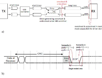
One of the techniques to deal with EMI issue in serial interfaces is using mutually coupled inductor choke. Choke placement is closer to the output of transmitter following USB2 connector as shown in fig. 1 a). The differential signalling through choke is adjusted for 50% cross-over minimizing common mode noise. This in turn reduces common mode noise induced electromagnetic interference. However when single ended transition occurs on differential lines as shown in fig. 1 b), the same choke generates overshoot and undershoots due to inductive kick back. The effect is severe for high slew rates. In USB2 standard communication protocol single edge transition occurs in SE0 state as shown in fig. 1 b). The SE0 state in high speed does not generate overshoot and undershoot to stress the devices because its small swing signalling, 400mV. However full speed is 3.3V signalling with highest possible slew rate of 4ns hence generates excessive overshoot and undershoots. The low speed is also 3.3V signalling but fastest slew rate is 20ns hence overshoot and undershoots are not generated. The generated overshoot and undershoots propagate down the line to receiver. At receiving end, transmitter is tri-stated and sees these overshoot and undershoots. The bulk, drain-source and drain-gate junction of 1.8V cascode transistor experience electrical over stress as depicted in fig. 2. As activity factor increases, the transistor devices see OS/US very often and degrade quite rapidly. This leads to change in device parameters like threshold voltage, transconductance
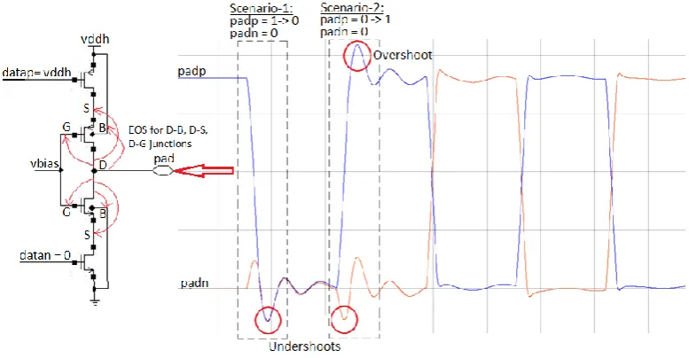
and thereby finally affects the transmitter output impedance. USB2 defines transmitter output impedance specification to be 45 +/- 5%. This specification may get violated over time leading to increased defects per million (DPM) number. To mitigate this reliability issue, EOS protection circuit is designed in Intel 22nm process. This EOS issue is divided in to two scenarios as shown in fig. 2. Scenario-1 is defined as padp making transition from high to low when padn is at logic low level. This scenario corresponds to undershoot on both padp and padn. Scenario-2 is defined as padp making transition from logic low level to logic high level and padn is still at logic low level. This scenario corresponds to overshoot on padp and undershoot on padn. These two scenarios occur due to tightly coupled two inductors of 200nH present in choke. Observed overshoot may go as high as 4.2V and undershoot as low as -0.6V. These voltage levels are high enough to violate the EOS limits of cascode devices of transmitter. Although not shown in fig. 3, there could be other structures connected to pads like receiver circuit, ESD protection circuit. These other devices/components connected to pad also undergo electrical stress and may degrade over time. This requires reliability simulations like “Aging” to determine amount of degradation over time and caused defects per million. Removing on board choke solves this EOS issue but results in to increased EMI. Alternative solutions to suppress EMI are not applicable USB2 application. For example Spread spectrum clocking for data bit stream may solve both EMI and EOS issue but violates the 500ppm requirement of USB2.
a)
b)
[image:2.595.120.476.71.344.2]
IV. PRINCIPLE OF OS/USSUPPRESSION
This invention detects overshoot & undershoot scenarios ahead of time and injects the charge in to pad when undershoot occurs and drains the charge from pad when overshoot occurs. The basic idea of charge injection and drain is illustrated in this section. Here we will be considering two different scenarios to address the issue. Scenario-1 is when padp makes transition from logic high to logic low and padn is at logic low level during EOP window. Scenario-2 is when padp makes transition from logic low level to logic high level and padn is at logic low level during EOP window.
a)
b)
Fig. 3. (a) Scenario-1 solution and (b) scenario-2 solution waveforms.
Scenario-1:(padp = 10, padn =0)
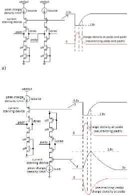
[image:3.595.107.496.59.261.2]this function is the total amount of charge injected as shown in fig. 3 a). The toal amount of charge injected can be controlled by peak current limiter and charge injection window length. The exact nature of charge density is controlled by controlling rise and fall slew at input of current starved devices. This input is exponential in nature and derived from output of RC circuit.
The charge injection mechanism is as illustrated in fig. 4 a). The constant current sources limits the peak charge density for controlled power consumption. The input to devices is slew controlled for rising edge to generate the required charge density profile. This rising slew is exponential in nature and generated by RC circuit. Thus injected charge in to pads lowers the undershoot.
a)
b)
Fig. 4. Implementation of (a) scenario-1 and (b) scenario-2 circuit.
Scenario-2:(padp = 01, padn =0)
As shown in fig. 3 b) the FSM part of this invention detects the SE0 condition of USB2 protocol where single edge transition occurs at the beginning of packet. Upon SE0 state detection it asserts start signal high. This start signal enables charge injection & drain circuit. The charge injection & drain circuit detects rising edge on padp and asserts end signal high.
The controlled amount of charge is drained from padp and injected in padn lowering the overshoot and undrshoot respectively. Once charge injection and drain action is over it asserts end signal low. This in turn causes start signal to go low disabling the charge injection & drain circuit. The total amount of charge injected/drained can be found by integrating charge density function. This can also be given as charge distribution function with respect to time. The final steady state value of this function is the total amount of charge injected/drained as shown in fig. 3 b). The toal amount of charge injected/drained can be controlled by peak current limiter and charge injection window length. The exact nature of charge density is controlled by controlling rise and fall slew at input of current starved devices. This input is exponential in nature and derived from output of RC circuit.
The charge injection & drain mechanism is as illustrated in fig. 4 b) where Isource and Isink are the constant current source and sink respectively. These sources limits the peak charge density for controlled power consumption. The input signals slew for current starving devices are exponential in nature and are adjusted by RC charging and discharging circuits. The slew timing is designed such a way that required charge injection & drain profile can be generated to partially neutralize the pad.
Under both scenarios the charge density and distribution function can be given by,
The total amount of charge injected/drained can be computed as
Since controlled amount of charge is injected/drained it results in controlled power consumption. This invention addresses issue exactly where it is needed (i.e. circuit not active on every edge) hence it provides optimum power solution.
V. EOSPROTECTION CIRCUIT
[image:4.595.43.300.255.645.2]schematic is as shown in fig. 9. The circuit operation is as explained below in reference to two different scenarios.
a)
b)
c)
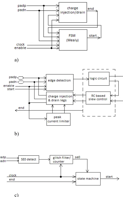
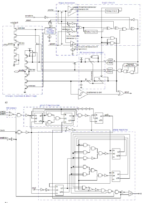
Fig. 5. (a) Top level block diagram of EOS protection circuit, (b) block diagram of charge injection/drain circuit , and (c) SE0 detect and finite state machine block diagram.
Scenario-1: (padp = 10, padn =0)
[image:5.595.55.291.96.473.2]In this scenario padn signal is low and padp signal transitioning from high to low is detected by low threshold detectors. The low threshold detectors are basic inverters tuned to threshold values which are very low. The detector on padp
Fig. 6. State diagram of Mealy type finite state machine.
has threshold of Vt1 and detector on padn has threshold value of Vt2. Here Vt2 is designed to be less than Vt1. The low threshold is achieved by making PMOS device weaker than NMOS device. Vt2 < Vt1 is ensured by making PMOS of detector-2 much weaker than PMOS of detector-1 and NMOS of 2 much stronger than NMOS of detector-1. Output of these detectors go low when signal goes above these threshold values. padp’ and padn’ are the inverted output of these signals as shown in fig. 3 a). The OR logic of these signals padp’ and padn’ goes low when padn is low and padp also goes low (crosses Vt1). XNOR logic of this signal with its delayed version gives output low. This is the window where charge injection & drain circuit is enabled and charge injection in to padp and padn is done to partially neutralize the pads. This in turn lowers undershoot. Here very precise detection of threshold values (~400mV) is not required and hence low power inverter based detectors are used.
Scenario-2:(padp = 01, padn =0)
[image:5.595.53.292.612.771.2]due to large range of rise time specification in Full speed (FS) mode of USB2 protocol. The rise time can be from 4ns to 20 ns in FS mode of USB2. These threshold circuits help to create window for charge injection & drain. Inverter based delay line is used to stretch this window further by some margin since overshoot lasts for ~5ns on padp after upper threshold detection. The charge injection & drain mechanism is as illustrated in fig. 4 where Isource and Isink are the constant current source and sink respectively. These sources limits the peak charge density. The input signal slew for current starving devices is adjusted by RC based charging and discharging circuits. The slew timing is designed such a way that required charge injection & drain profile can be generated to partially neutralize the pad. The capacitors in RC circuit are implemented as MOS caps and resistors by poly. The poly resistor variation is minimized by six bit calibration code. This improves precision of charging and discharging time bases generated by RC circuits. The peak injected & drained charge density becomes very high under fast corner and damps the overshoot to very low value. This unnecessarily increases power consumption and results in overdesign. This invention limits the peak current optimizing design for power consumption.The peak current limit circuit is basic current mirror circuit which takes in constant current and mirrors to charge injection & drain legs so that peak current never exceeds certain value under fast process corner. The charge injection & drain circuit uses level shifter to shift input signalling levels from 0V ->1.8V to 1.8V -> 3.3V for PMOS devices comprising charge injection leg. This level shifting is necessary because the devices used are 1.8V devices in 3.3V domain.
Power advantage:
USB2.0 specification [5] defines FS frame interval to be 1ms and USB2.0 FS speed = 12Mbps [UI=83.33ns] => 1ms/83.33ns = 12000 bits/frame
USB2.0 spec, max transfers/frame = 150
Hence 150 EOP events in 1ms frame (OS/US happens only during EOP).
[image:6.595.304.550.443.762.2]
Fig. 7. USB2.0 FS data packet format.
i.e. 150 EOP events for 12000 bits => 1-EOP/80bit
Total active power consumption of this EOS protection circuit is 4.6mW under worst case PVT. The comparator is the only static power consuming block which consumes 0.2mW of power. Remaining 4.4mW of switching/dynamic power is consumed by state m/c and other sub blocks.
Hence 1-EOP/80 bits => 4.6mW/80bits => 57.5uW/bit
Assume 1-EOP/1000bits => 4.6mW/1000bits => 4.6uW/bit
This unique combination of analog, digital components and intelligence (FSM) differentiates it from conventional architectures. The added intelligence (FSM) saves significant amount of power since it enables circuit only when required.
VI. SIMULATION RESULTS
A test set up shown in fig. 1 a) is prepared with appropriate SPICE models for different components [6] and simulations are run. The test set up is comprised of
1. TX modelled as ideal pulse generator and 45 impedance with +/-5% tolerance.
2. Short traces modelled by transmission line model
3. USB connector model
4. Choke model
5. Long, 14-inch trace modelled by transmission line model
6. RX modelled by 10pF in parallel with 15K-Ohm
7. EOS Protection Circuit in Intel 22nm process
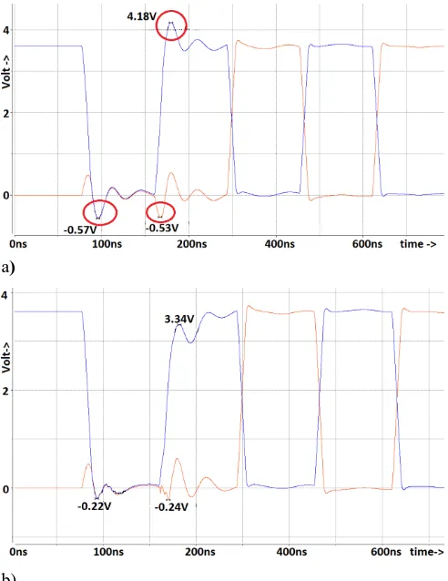
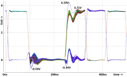
Fig. 8 a) shows overshoot and undershoot caused by on board choke during SE0 EOP window in full speed mode. The observed overshoot is 4.2V and undershoot is -0.6V. Fig. 8 b) shows reduced overshoot and undershoot by proposed EOS protection circuit. In typical conditions overshoot and undershoot is reduced to 3.3V and -0.24V respectively. Fig. 10 shows worst case, across all PVT conditions overshoot and undershoot reduced as low as 3.7V and -0.34V respectively.
a)
b)
[image:6.595.46.298.549.652.2]a)
b)
[image:7.595.74.531.62.712.2]Fig. 10. PVT simulation result with EOS protection circuit.
PVT conditions consider all 15 corners, 10% variation on 1.8V & 3.3V supply, and Temperature variation from -40oC to 125oC.
VII. CONCLUSION
This paper demonstrates design solution to address emerging issues with advanced sub-micron process technology. It uses some intelligence to detect the EOS issue and addresses exactly where and when it’s needed. This makes it very low power design. This EOS protection circuit can be used for future submicron technologies like 14nm, 10nm and onwards.
ACKNOWLEDGMENT
The author wishes to thank Intel Microelectronics, HIP USB2 circuit team, Malaysia for providing necessary access to tools and Intel 22nm process technology. Author also would like to thank IMC WPRD ETS DSI IPR PHY group, Germany for their encouragement and support on this work.
REFERENCES
[1] Inventor: Suhas Vishwasrao. Shinde, Patent application filed, PCT/US2011/059229.
[2] M. Morris Mano, “Digital Design”, Prentice Hall, 2002.
[3] Behzad Razavi, “Design of Analog CMOS Integrated Circuits”, McGraw-Hill, (2001).
[4] P.E. Allen, D.R. Holberg, CMOS Analog Circuit Design, Holt, Reinhart, and Winston, Inc., 1987.
[5] Universal Serial Bus Revision 2.0 specification, USB.org