TOPICAL COLLECTION: INTERNATIONAL CONFERENCE ON THERMOELECTRICS 2018
Doping Optimization for the Power Factor of Bipolar
Thermoelectric Materials
SAMUEL FOSTER 1,2and NEOPHYTOS NEOPHYTOU1
1.—School of Engineering, University of Warwick, Coventry CV4 7AL, UK. 2.—e-mail: [email protected]
Bipolar carrier transport is often a limiting factor in the thermoelectric effi-ciency of narrow bandgap materials at high temperatures due to the reduction in the Seebeck coefficient and the introduction of an additional term to the thermal conductivity. Using the Boltzmann transport formalism and a two-band model, we simulate transport through bipolar systems and calculate their thermoelectric transport properties: the electrical conductivity, the Seebeck coefficient and the thermoelectric power factor. We present an investigation into the doping optimisation of such materials, showing the detrimental impact that rising temperatures have if the doping (and the Fermi level) is not optimised for each operating temperature. We also show that the doping levels for optimized power factors at a given operating temperature differ in bipolar systems compared to unipolar ones. We show finally that at 600 K, in a bipolar material with bandgap approximately that of Bi2Te3, the
optimal doping required can reside between 10% and 30% larger than that required for an optimal unipolar material depending on the electronic scat-tering details of the material.
Key words: Thermoelectrics, thermoelectric power factor, bipolar transport effects, Seebeck coefficient, optimized doping, Boltzmann transport theory
INTRODUCTION
The efficiency of thermoelectric (TE) materials (which convert between heat and electricity) is quantified by the figure of meritZT=rS2T/(jl+je)
where r is the electrical conductivity, S is the Seebeck coefficient, T is temperature, jl is the
lattice thermal conductivity andjeis the electronic
thermal conductivity. The quantity rS2 is termed the power factor (PF).
Many of the most important TE materials are narrow bandgap semiconductors.1 These narrow bandgaps (e.g., PbTe0.3 eV,2Bi2Te30.2 eV,3 SnSe0.39
eV)4mean the materials suffer from bipolar effects at high operating temperatures. The bipolar effect occurs when both electrons and holes contribute to charge
transport. When this happens: (1)jeincreases due to
contributions from both electrons and holes, (2) an additional thermal conductivity term, the bipolar ther-mal conductivity,jbi, is introduced (a result of electron–
hole recombination at the contacts),5which also intro-duces large increases in the Lorenz number,6(3) the Seebeck coefficient drops as both electrons and holes contribute to it with opposite signs, and (4) the Fermi level moves towards the midgap in order to conserve carrier concentration, (although it does not fall as quickly as in the unipolar case). The thermal conduc-tivity from (1) and (2) degrades thermoelectric perfor-mance through the denominator of ZT, whereas (3) degrades performance through the numerator.
The optimal thermoelectric performance (for both the peak PFand peak ZT) depends heavily on the carrier concentration,7and this optimal is known to be temperature dependent, i.e., the performance peaks at different doping concentrations for differ-ent temperatures.8 However, although it is known
(Received August 23, 2018; accepted December 4, 2018)
that for unipolar materials the optimized doping increases as T3=2,9
the optimization of the carrier concentration for bipolar systems is not yet clarified. While various strategies have been suggested to reduce the bipolar effect in order to regain high performance, such as using heterostructure designs,10,11 band engineering to widen the band-gap,12,13 and grain boundaries with barriers for minority carriers,14 in this work we show that considering proper doping optimization by taking into account the bipolar effects could also allow for performance improvements.
For this, in this work we use Boltzmann transport theory and a two-band model (conduction and valence band) to examine the impact of the bipolar effect on the thermoelectric transport coefficients (r,S, and thePF), as well as its effect on the optimal carrier concentra-tion and doping. We show that the typical models and trends employed in the literature for optimal doping concentrations for maximizing the power factor and ZT for a unipolar material are no longer valid in bipolar materials. We show that optimising the carrier concentration for the operating (higher) temperatures can provide significant increases in the power factor andZTcompared to maintaining a low temperature optimised carrier concentration.
APPROACH
To calculate the thermoelectric coefficients we use the linearized Boltzmann transport formalism. In this method the electrical conductivity (r), the Seebeck coefficient (S) and the electronic thermal conductivity (je) are given by
15,16
r¼q20 Z1
1
dE @f
@E
Nð ÞE ; ð1Þ
S¼q0kB
r
Z1
1
dE @f
@E
Nð ÞE EEF kBT
; ð2Þ
je ¼k2BT Z1
1
dE @f
@E
NðEÞ EEF kBT
2
rS2T;
ð3Þ
whereq0is the elementary charge,Eis energy,fis
the Fermi–Dirac distribution, kB is the Boltzmann
constant, and EF is the Fermi level. The quantity N(E) is called the transport distribution function and is defined as
Nð Þ ¼E v2ð ÞEsð Þg EE ð Þ; ð4Þ
where v is the bandstructure velocity, s is the relaxation time and gis the density of states. Here we use the 3-D density of states under an isotropic parabolic band approximation:
g Eð Þ ¼m
3=2
p2h3
ffiffiffiffiffiffiffiffiffiffiffiffiffiffiffiffiffiffiffiffiffiffiffiffiffiffiffi 2 EEC=V
q
; ð5Þ
where m* is the effective mass, h is the reduced Planck’s constant, and EC/V is the
conduction/va-lence band edge.
Acoustic phonon scattering (ADP) is considered under a relaxation time approximation, according to
1
s¼ pD2
AkBT
hcl
gðEÞ; ð6Þ
where we useDA= 5 eV for the acoustic deformation
potential as in typical semiconductors, andcl= 1.908
91011kgm1 s2is the elastic constant.17
Ionised impurity scattering (IIS) is included according to the Brooks-Herring model:
s¼16 ffiffiffiffiffiffiffiffiffi 2m
p
pe2 re20 NIq4
lnð1þc2Þ c 2
1þc2
1
E3=2; ð7Þ
where er is the relative permittivity, e0 is the
permittivity of free space, NI is the density of
impurities andc28mEL2 D
.
h2;where
LD¼
ffiffiffiffiffiffiffiffiffiffiffiffiffiffiffiffiffi
ere0kBT q2
0NI s
ð8Þ
is the Debye screening length.17
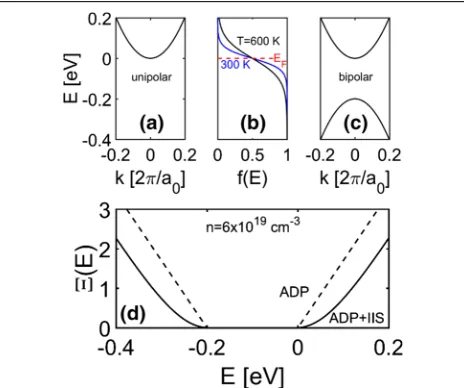
We consider two bandstructures as show in Fig.1: (1) a single parabolic conduction band with effective
Fig. 1. (a) The unipolar case: a single parabolic conduction band with effective massmC=m0and conduction band edgeEC= 0 eV,
(b) the Fermi distribution at T= 300 K (blue line) and T= 600 K (black line) with EF= 0 eV (red-dashed line), and (c) the bipolar
case: a single parabolic conduction band with effective mass
mC=m0andEC= 0 eV and a single parabolic valence band with
effective mass mV=m0 and EV=0.2 eV. In (d) we show the
transport distribution function versus energy for the bipolar material for two different scattering regimes: acoustic phonon scattering (dashed line), and acoustic phonon scattering and ionised impurity scattering for an impurity density ofn= 691019cm3(solid line)
[image:2.594.305.537.427.621.2]mass mC=m0 where m0 is the electron rest mass,
and conduction band edgeEC= 0 eV (unipolar case,
Fig.1a); and (2) a bipolar system with a single parabolic conduction band with effective massmC=
m0 and EC= 0 eV and a single parabolic valence
band with effective mass mV=m0 and EV=0.2
eV (bipolar case, Fig.1c). The bandgap of the bipolar system (Eg= 0.2 eV) is similar to that of
Bi2Te3, for example.
RESULTS
Most thermoelectric materials have complex band-structures and even more complex scattering mech-anisms, however, in this study we only employ the single band effective mass approximation, which can give us simple first order guidance towards doping optimization in bipolar materials, putting aside complexities that arise from multi-band features.
We begin by ‘scanning’ the Fermi level,EF, across
the unipolar and the bipolar bandstructure materi-als in order to identify the optimal values of the power factors andZTand the optimal positioning of the Fermi level (meaning that we compute the thermoelectric coefficients for a series ofEF values,
eachEF corresponding to a specific doping
concen-tration). We first consider the case in which trans-port is limited by acoustic phonon scattering (ADP) and then include ionised impurity scattering in addition (ADP + IIS). As we will show, the obser-vations are different in the two cases.
In Fig.2a and b we show thePFversusEFfor (a)
the unipolar case, and (b) the bipolar case under ADP limited scattering at four different
temperatures: T= 300 K (blue lines), T= 400 K (green lines), T= 500 K (red lines), T = 600 K (black lines). In the unipolar case it can be seen that thePFpeaks are just above the band edge (at approximately EC= 0 eV) as previously suggested
in earlier studies.18–20 The Fermi level value at which this occurs increases linearly with tempera-ture (a small shift only is evident here since the transition happens around 0 eV), but the peak PF remains constant. This behaviour will be discussed in more detail later. In the bipolar case (Fig.2b) the PFpeak for both bands moves even further into the band with increasing temperature. A small decrease is also unavoidable as the increasing contribution of holes from the valence band reducesS. Importantly, however, thePFpeaks in both cases are spread over increasingly wider EF values with increasing
tem-perature (the black lines are broader compared to the blue lines), meaning that the power factor is somewhat more resilient to changes in carrier concentration at higher temperatures. In Fig.2c we show ZT versus EF for the bipolar case only
(considering only je, with jl= 0 for brevity, but
which allows us to observe the peaks limiting case at very low jl versus the limit of large jl, which
follows the power factor trend). We do not show the unipolar case since, because je/r in the non-degenerate limit, the quantity ZT¼rS2
je diverges at
[image:3.594.55.550.457.664.2]low carrier concentrations, following the rise in S. In the bipolar case, the peak occurs closer to the midgap than when the PF only is considered, although it also then rises more quickly with temperature as discussed later.
Fig. 2. The power factor versus Fermi level at four different temperatures: 300 K (blue lines), 400 K (green lines), 500 K (red lines), 600 K (black lines) for (a) a single parabolic conduction band withEC= 0 eV andmC=m0, under acoustic phonon scattering conditions (ADP), (b) a bipolar
system with one parabolic conduction band withEC= 0 eV andmC=m0, and one parabolic valence band withEV=0.2 eV andmV=m0under
acoustic phonon scattering conditions, (d) a single parabolic conduction band withEC= 0 eV andmC=m0, under acoustic phonon and ionised
impurity scattering conditions (ADP + IIS), and (e) a bipolar system with one parabolic conduction band withEC= 0 eV andmC=m0, and one
parabolic valence band withEV=0.2 eV andmV=m0under acoustic phonon and ionised impurity scattering conditions. In (c) and (f) we show
Although we considered ADP scattering alone, the high carrier concentration in TE materials is achieved by impurity doping, which introduces a strong, possibly dominant scattering mechanism in common semiconductors. Therefore, in Fig. 2d, e and f we further show the same three Fermi ‘scans’ in the presence of both acoustic phonon scattering and ionised impurity scattering (indicated as ADP + IIS). The introduction of an additional scattering mechanism reduces the power factor. However, as the temperature rises, in the ADP + IIS case the peak power factor value now increases with tem-perature in both the unipolar and bipolar cases. In the case of optimising ZT, the peaks again occur closer to the midgap (as in the ADP limited results); however, the peak values are now higher in value. This is because, as seen in the transport distribution function shown in Fig.1d, the introduction of the IIS affects low energy electrons more heavily than higher energy electrons. Since the Seebeck coeffi-cient is proportional to the average energy of the current flow as S/h i E EF this results in an increase in the Seebeck coefficient (comparing at a fixedEF). In addition, this also results in a widening
of the ‘effective transport bandgap’ (although these states are available they contribute significantly less to transport). This then results in a decrease in the bipolar effect giving an additional increase toS as well as a reduction inje. Hence, the values ofZT
increase with the addition of IIS.
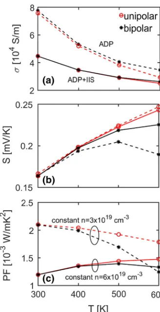
To show the behaviour of the power factor as the temperature rises, we next take the bandstructures we consider with carrier concentration optimised at T = 300 K and examine how the thermoelectric coefficients change when that carrier concentration is kept fixed at theT= 300 K optimal value. This is in order to replicate the constant doping concentra-tions found in experimental set-ups. Figure 3shows
r, SandPFversusTfor the unipolar (red lines) and bipolar (black lines) bandstructures for the cases of acoustic phonon scattering only (ADP, dashed lines) and acoustic phonon plus ionised impurity scatter-ing (ADP + IIS, solid lines). Note that the optimal carrier concentration is different in the case of ADP and ADP + IIS situations, n= 391019 cm3 and n = 691019cm3, respectively. As the tempera-ture increases and the Fermi distribution broadens, EF drops in order to satisfy charge neutrality. The
EFdecrease is limited in the bipolar case due to the
increasing contribution of holes to the total carrier concentration, which counteract the downshift of the EF. The electrical conductivity decreases with
temperature for two reasons: (1) the acoustic phonon scattering strength is proportional to T (see Eq.6), (2) EF moves towards the midgap
meaning lower velocity states are participating to transport. In the unipolar case (red lines), the Seebeck coefficient shows an increase with T since it is proportional to the difference between the average energy of the current and the Fermi level, S/h i E EF. The quantity h i E EF increases in
the unipolar case due to the significant drop inEF
with T. In the bipolar case, however, the Seebeck coefficient increases to a lesser extent compared to the unipolar case (and even eventually begins decreasing) due to the increase in holes which contribute to Swith opposite sign to the electrons. The resultant effect on the power factor from these behaviours is: (1) in the unipolar ADP case (red dashed line), a decrease of 15% from 300 K to 600 K is observed, (2) in the bipolar ADP case (black dashed line), despite the smaller reduction in r at 600 K from the extra contribution to current that the valence band provides, there is an overall degradation in the power factor by40% which is much more significant than in the unipolar case.
[image:4.594.337.501.63.382.2]With the introduction of IIS for both unipolar and bipolar channels,rnaturally drops due to the extra scattering rate. However, as expected, at higher temperatures this drop is not as substantial as in the ADP case as the IIS scattering typically weak-ens with temperature. This is due to the broadening of the Fermi distribution (see Fig.1b) and the occupation of higher energy states with larger
Fig. 3. The (a) electrical conductivity, (b) Seebeck coefficient, and (c) power factor versus temperature at constant carrier concentration for two bandstructures: a single parabolic conduction band of mass
mc=m0, (red lines), and a bipolar system with one conduction and
one valence band with massesmc=m0,mv=m0(black lines), and
bandgap Eg= 0.2 eV. Results are shown for acoustic phonon
wavevectors which are less impacted by IIS. This can again be seen from the IIS stronger impact on the transport distribution function at lower energies in Fig.1d. The improvement in r from the valence band contribution in the ADP case in the bipolar channel (comparing red-dashed to black-dashed lines in Fig.3a) is now also missing in the ADP + IIS lines due to the widening of the ‘effective transport bandgap’ that IIS causes as explained earlier, and effectively makes the material ‘look’ more unipolar (Fig.1d).
When it comes to the Seebeck coefficient in Fig.3b and the introduction of IIS, bipolar trans-port no longer has such a strong effect on S with increasing temperatures, due to this widening of the ‘effective transport bandgap’ due to IIS, unlike in the ADP-limited case (solid versus black-dashed line in Fig.3b). The result of these effects on thePF, therefore, is a significant reduction at low temperatures compared to the ADP-limited case, but an increase with temperature (Fig.3c). The increase is a consequence of the smaller relative reduction inr and the continuous rising ofS.
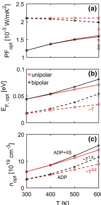
Figure3shows and explains why the power factor drops (in the ADP case) or increases less that its optimal value if the carrier concentration (con-trolled by doping) remains at theT= 300 K optimal levels. We now show that the power factor can be improved by a careful optimisation of the carrier concentration at higher temperature operations. In Fig.4a we show the optimalPFof the unipolar (red lines) and bipolar (black lines) bandstructures for the cases of ADP scattering only (dashed lines) and ADP + IIS (solid lines), i.e., the peaks of the Fermi scans seen in Fig.2.
For ADP scattering only, whereas the unipolar system previously saw a reduction of 15%, by optimising the doping with temperature the power factor now remains constant (Fig.4a—red-dashed line). In the bipolar case the dramatic fall in the power factor due to the Seebeck reduction (as seen previously in Fig.3b, black-dashed line) is miti-gated by increasing the Fermi level. Consequently the power factor, although still slightly decreasing with temperature, is now 60% higher at 600 K than in the un-optimised case from Fig.3c (un-optimised values from Fig.3c shown by the square markers at 600 K in red (unipolar) and black (bipolar).
The Fermi level required to produce these optimal values rises linearly with temperature in the unipo-lar system (red-dashed line in Fig.4b). This beha-viour was earlier identified by Ioffe in Ref.9where it was shown that the optimal reduced Fermi level
gF,opt= (EFEC)/kBT=r, where r is an exponent
that depends on the electron scattering mechanism. Sinceris a constant, this givesEF/T. In our case of acoustic phonon scattering r= 0, so we would expect the power factor to peak at the band edge. However, Ioffe’s derivation assumes Boltzmann statistics for the carrier distribution and, indeed,
running our calculations under that assumption reproduces such a result (not shown). However, using the more accurate (for degenerate doping conditions) Fermi–Dirac distribution, we find that in the case of acoustic phonon scatteringgF,opt2/3.
In the bipolar system the linear behaviour seen in the unipolar case no longer holds, and the optimum Fermi level rises quicker than linearly (black-dashed line in Fig.3b). This is in order to avoid the detrimental impact of the bipolar effect that the valence band introduces.
In Fig. 4c we also show the optimal carrier concentration required to set EF at the optimal
position. As has been previously identified in the literature,9,21the optimal carrier concentration in a unipolar system increases as nopt/T3=2 (red-dashed line). Again, however, in the bipolar system (black-dashed line) the unipolar behaviour no longer holds, and the required carrier concentration rises more quickly in order to produce the higher Fermi levels seen in Fig.4b, following an
Fig. 4. The optimal values of (a) the power factor, (b) Fermi level, and (c) carrier concentration versus temperature for two bandstructures: a single parabolic conduction band of massmc=m0, (red lines), and a
bipolar system with one conduction and one valence band with masses
mc=m0,mv=m0(black lines), and bandgapEg= 0.2 eV. Results are
[image:5.594.353.516.65.394.2]approximate T1:8 trend. Indeed, at T = 600 K the optimal bipolar carrier concentration is 30% higher than the optimal unipolar carrier concentration.
When IIS is included, the power factor values are lower as explained previously, but increase with increasing temperature due to the occupation of higher energy states which scatter less under IIS. Benefits compared to the un-optimised values (dia-mond markers in Fig. 4a) are not as great as in the ADP only case, but still significant—10% for the unipolar bandstructure and 20% for the bipolar bandstructure (solid lines in Fig.4a). The Fermi level and carrier concentration values needed to achieve these power factor values are higher than in the ADP only case. For practical purposes, there-fore, to achieve an optimized power factor in the bipolar case at T = 600 K in the material we consider of bandgap Eg = 0.2 eV, the doping
con-centration needs to be by 160% higher compared to the value that provides optimizedPFatT= 300 K. That value is by 10% higher compared to the one that achieves the optimal T= 600 K PF in the unipolar case. Note that in the case of the ADP + IIS transport conditions, the optimal doping den-sity is higher, due again to the widening of the ‘effective transport bandgap’ seen in Fig.1d. Also note that these values are to be altered in the case of a different bandgap, i.e., the relevance of these values are shifted to lower/higher temperatures as the bandgap decreases/increases.
Finally, due to the influence of the thermal conductivity in the denominator of ZT, which has its own temperature dependence, ZTdoes not peak
at the same EF or carrier concentration as thePF.
Therefore, in Fig.5we compare the optimal carrier concentration and Fermi levels when optimising for the power factor (same black lines as in Fig.4b and c) and optimising forZT(green lines). This compar-ison here is shown only for the bipolar material since the unipolar material does not show a peak as explained previously. For the calculation of ZT we consider only the electronic properties (i.e., we take
jl= 0, as the behaviour ofjl is material dependent
and more complex). Sinceje/rthrough the Lorenz number,jeis reduced with fallingEFand, therefore,
the peaks inZToccur at significantly lower density andEFthan when just optimising for thePF. As the
temperature is increased, however, the optimal values (in both ADP and ADP + IIS cases) rise at a quicker pace than when optimising forPF. This is because as the temperature increases the impact of the bipolar effect kicks in and jbi increasingly
pushes the peak away from the midgap. The intro-duction of IIS, however, when optimising forZThas much less influence than in when optimising for the PF. This is again due tojebeing proportional tor. As
can be seen in Fig.3, the introduction of IIS primarily affectsr. When optimising forZT, this impact is then cancelled out by the same impact onje.
Of course in a real materialjl 6¼0 and the optimal ZT values will lie somewhere between the PF-optimised and our jl= 0 ZT-optimised values. In
particular, it is interesting to note that the smaller the value ofjlin the material with respect to theje,
the closer it is to thejl= 0ZT-optimised case, and,
therefore, the less it needs to be doped to reach its optimal ZT, which can prove helpful for TE mate-rials, as doping at extremely high values can prove difficult in many cases.
Finally, we would like to state that in this work we employed a simple two-band parabolic model to obtain first order optimization strategies for doping in bipolar TE materials. In reality, material band-structures are typically more complex than the simple two-band parabolic model we assume here. Real material bandstructures can have a variety of band gaps, effective masses, band degeneracies, band non-parabolicity, and multiple valence and/or conduction bands. Many of these bandstructure features can also vary with temperature, and detailed studies on each material are essential for proper optimization. In this study, however, it was our aim to demonstrate to first order the important, yet overlooked, impact of the bipolar effect on the doping optimisation.
CONCLUSIONS
[image:6.594.39.270.438.677.2]Using the Boltzmann transport formalism we have calculated the thermoelectric transport coeffi-cients for unipolar and bipolar systems and pre-sented a study on the optimal doping conditions for the power factor and ZT figure of merit. We have shown that, if the carrier concentration is not
properly optimised at the temperature of operation, but room temperature optimal doping is consid-ered, the power factor can underperform by 15% in the unipolar systems, and 40% in the bipolar system under ADP scattering, and 10% in the unipolar systems, and 20% in the bipolar system under ADP + IIS scattering. Consequently, signifi-cant enhancements in the PF (40%) can be achieved through doping optimisation. Furthermore we have identified that in a bipolar system the optimal carrier concentration indicates an approxi-matelyT1:8trend, larger compared to theT3=2trend in unipolar materials, a result of the additional degradation due to bipolar transport. In our simula-tions, the optimal carrier concentration atT= 600 K in a material with bandgapEg= 0.2 eV (e.g.,
approx-imately that of Bi2Te3) then becomes 30% larger than
expected from the unipolar calculation. We believe that our findings will be useful in the optimal design of bipolar thermoelectric materials.
ACKNOWLEDGMENTS
This work has received funding from the Euro-pean Research Council (ERC) under the EuroEuro-pean Union’s Horizon 2020 Research and Innovation Programme (Grant Agreement No. 678763).
OPEN ACCESS
This article is distributed under the terms of the Creative Commons Attribution 4.0 International License (http://creativecommons.org/licenses/by/4.0/), which permits unrestricted use, distribution, and reproduction in any medium, provided you give appropriate credit to the original author(s) and the source, provide a link to the Creative Commons license, and indicate if changes were made.
REFERENCES
1. G. Prashun, S. Vladan, and E.S. Toberer,Nat. Rev. Mater.2, 17053 (2017).
2. L.-D. Zhao, H.J. Wu, S.Q. Hao, C.I. Wu, X.Y. Zhou, K. Bis-was, J.Q. He, T.P. Hogan, C. Uher, C. Wolverton, V.P. Dravid, and M.G. Kanatzidis,Energy Environ. Sci.6, 3346 (2013).
3. H. Goldsmid,Materials7, 2577 (2014).
4. L.-D. Zhao, V.P. Dravid, and M.G. Kanatzidis, Energy Environ. Sci.7, 251 (2014).
5. M. Lundstrom,Notes on Bipolar Thermal Conductivity(2017).
https://nanohub.org/groups/ece656_f17/File:Notes_on_Bipola r_Thermal_Conductivity.pdf. Accessed 11 June 2018. 6. M. Thesberg, H. Kosina, and N. Neophytou,Phys. Rev. B95,
125206 (2017).
7. G. Snyder and E. Toberer,Nat. Mater.7, 105 (2008). 8. Q. Zhang, Q. Song, X. Wang, J. Sun, Q. Zhu, K. Dahal, X.
Lin, F. Cao, J. Zhou, S. Chen, G. Chen, J. Mao, and Z. Ren, Energy Environ. Sci.11, 933 (2018).
9. A.F. Ioffe, Semiconductor Thermoelements, and Thermo-electric Cooling(London: Infosearch Ltd., 1957).
10. P.G. Burke, B.M. Curtin, J.E. Bowers, and A.C. Gossard, Nano Energy12, 735 (2015).
11. J.-H. Bahk and A. Shakouri,Phy. Rev. B93, 165209 (2016). 12. H.-S. Kim, K.H. Lee, J. Yoo, W.H. Shin, J.W. Roh, J.-Y. Hwang, S.W. Kim, and S.I. Kim,J. Alloys Compd741, 869 (2018).
13. L. Zhang, P. Xiao, L. Shi, G. Henkelman, J.B. Goodenough, and J. Zhou,J. Appl. Phys.117, 155103 (2015).
14. B. Poudel, Q. Hao, Y. Ma, Y. Lan, A. Minnich, B. Yu, X. Yan, D. Wang, A. Muto, D. Vashaee, X. Chen, J. Liu, M.S. Dresselhaus, G. Chen, and Z. Ren,Science320, 634 (2008). 15. G. Mahan and J.O. Sofo,Proc. Natl. Acad. Sci. USA93, 7436
(1996).
16. T.J. Scheidemantel, C.A. Draxl, T. Thonhauser, J.V. Bad-ding, and J.O. Sofo,Phys. Rev. B68, 125210 (2003). 17. M. Lundstrom,Fundamentals of Carrier Transport
(Cam-bridge: Cambridge University Press, 2000).
18. S. Foster, M. Thesberg, and N. Neophytou,Phys. Rev. B96, 195425 (2017).
19. N. Neophytou and M. Thesberg,J. Comput. Electron.15, 16 (2016).
20. C. Jeong, R. Kim, and M. Lundstrom,J. Appl. Phys.111, 113707 (2012).