warwick.ac.uk/lib-publications
Original citation:Sanchez, Ana M., Gott, James A., Fonseka, H. Aruni, Zhang, Yunyan, Liu, Huiyun and Beanland, Richard (2018) Stable defects in semiconductor nanowires. Nano Letters, 18 (5). pp. 3081-3087. doi:10.1021/acs.nanolett.8b00620.
Permanent WRAP URL:
http://wrap.warwick.ac.uk/101003
Copyright and reuse:
The Warwick Research Archive Portal (WRAP) makes this work by researchers of the University of Warwick available open access under the following conditions. Copyright © and all moral rights to the version of the paper presented here belong to the individual author(s) and/or other copyright owners. To the extent reasonable and practicable the material made available in WRAP has been checked for eligibility before being made available.
Copies of full items can be used for personal research or study, educational, or not-for profit purposes without prior permission or charge. Provided that the authors, title and full bibliographic details are credited, a hyperlink and/or URL is given for the original metadata page and the content is not changed in any way.
Publisher’s statement:
This document is the Accepted Manuscript version of a Published Work that appeared in final form in ACS Sustainable Chemistry & Engineering, copyright © American Chemical Society after peer review and technical editing by the publisher.
To access the final edited and published work see link to Published Work, see: https://doi.org/10.1021/acs.nanolett.8b00620.
A note on versions:
The version presented here may differ from the published version or, version of record, if you wish to cite this item you are advised to consult the publisher’s version. Please see the ‘permanent WRAP URL’ above for details on accessing the published version and note that access may require a subscription.
2
Stable Defects in Semiconductor Nanowires
A. M. Sanchez§, J. A. Gott§, H. A. Fonseka§, Y. Zhang†, H. Liu† and R. Beanland§
§ Department of Physics, University of Warwick, Coventry CV4 7AL, United Kingdom
†Department of Electronic and Electrical Engineering, University College London, Torrington Place,
London WC1E 7JE, United Kingdom
Abstract:
Semiconductor nanowires are commonly described as being defect-free due to their ability to
expel mobile defects with long-range strain fields. Here, we
describe previously undiscoveredtopologically-protected line defects with null Burgers vector that, unlike dislocations, are stable in
nanoscale crystals. We
analyse the defects present in semiconductor nanowires in regions of
imperfect crystal growth, i.e. at the nanowire tip formed during consumption of the droplet in
self-catalysed vapour-liquid-solid growth and subsequent vapour-solid shell growth. We use
a form of the Burgers circuit method that can be applied to multiply-twinned material without
difficulty. Our observations show that nanowire microstructure is very different from bulk
material, with line defects either a) trapped by locks or other defects, b) arranged as dipoles or
groups with zero total Burgers vector or c) having zero Burgers vector. We find two new line
defects with null Burgers vector, formed from the combination of partial dislocations in
twinned material. The most common defect is the three-monolayer high twin facet with zero
Burgers vector. Studies of individual nanowires using cathodoluminescence shows that optical
emission is quenched in defective regions, showing that they act as strong non-radiative
recombination centres.
3 Continuous innovation and growth have given semiconductor materials and devices a fundamental role in the modern world. Despite this success, one of the key problems that remains to be convincingly solved is the inability to combine different materials, due to fundamental problems such as lattice mismatch and differences in thermal expansion coefficients. These produce defects including dislocations and cracks that prevent devices from operating or make them unreliable. Recently, the one-dimensional nanowire (NW) geometry has gained increasing attention in comparison with its two-dimensional thin film counterpart, with more and more devices being successfully demonstrated using nanowire based architectures.1-5 One of the main reasons for the
interest in nanowires is their inherent ability, in principle, to grow as perfect crystals. The influence of the substrate on a NW is minimal, since it is attached by only a small area at its base. The inherent crystal perfection of nanowires comes as a result of their small volume and relatively large surface area, which produces strong image forces on any defects with a long-range strain field.6. Hence,
mobile defects should be expelled from the interior of the nanowire. The commonly seen layer-by-layer growth of the nanowire in vapour-liquid-solid (VLS) produces highly perfect material.7
Growth strategies are improving and device structures are being explored for semiconductor nanowires, but one of the remaining difficulties is how to remove or convert the catalyst droplet into a different form after growth. Consumption of a Ga catalyst particle in self-catalysed nanowires to produce GaAs appears to be an elegant solution8 and allows subsequent production of core-shell
structures. This may result in other growth modes have been observed, e.g. multiple facet wetting, multiple nucleation sites at the catalyst droplet/nanowire interface, three-dimensional nucleation, and non-planar/truncated growth interfaces.9, 10, 11 An obvious question is whether the small size of
4 performance and reliability. For this reason, it is important to understand the stable defects that may originate from imperfect nanowire growth.
Here, we present an extensive survey of defects in zinc blende III-V NWs. Different types of defects, seen in the tips of GaAsP-GaAsP self-catalysed core-shell nanowires whose Ga catalyst droplets have been consumed in the growth process, are analysed in terms of their Burgers vectors, interaction with each other and relative frequency of occurrence. The microstructure is quite distinct from that of bulk material and unconventional types of defect are found. The analysis provides an explanation of the stable existence of line defects within the small volume of the nanowires.
GaAsP core NWs were grown with a Ga beam equivalent pressure, V-to-III flux ratio, P/(As +
P) flux ratio, substrate temperature, and growth duration of 8.41 × 10⁻⁸ Torr, 40, 12%, ∼640 °C and
1h, respectively. After the NW growth, the droplets were consumed for 30mins by closing the Ga flux
and increasing the group-V flux to ~8× 10⁻⁶ Torr. After that the temperature was reduced to ∼400 °C
and the GaAsP shell was grown with a Ga beam equivalent pressure, V-to-III flux ratio, P/(As + P) flux
ratio, and growth duration of 8.41 × 10⁻⁸ Torr, 50, 30%, , and 60 min, respectively.
A simple scraping of the NWs onto a lacy carbon support was used to prepare transmission electron microscopy (TEM) specimens. STEM analysis was performed on a doubly corrected ARM200F microscope operating at 200 kV. ADF-STEM images were obtained using a JEOL annular field detector using a fine-imaging probe, at a probe current of approximately 23 pA with a convergence semiangle of ∼25 mrad. Optical properties were investigated using cathodoluminescence spectroscopy at ~-100°C using a Gatan MonoCL4 spectrometer attached to a Zeiss Supra 55VP SEM operating at 5kV (using a spectral resolution of 2nm).
BURGERS VECTORS
5 growth. Each atom column is clearly resolved, allowing the structure to be seen in full detail. While it is clear in Fig. 1a that there are multiple twins and different interfaces and structures, it is not immediately apparent if any of them have a long-range strain field (i.e. have a Burgers vector component that could be detected, in the plane of the image). Thus, before considering the different defect types observed, we set out a general framework for their analysis.
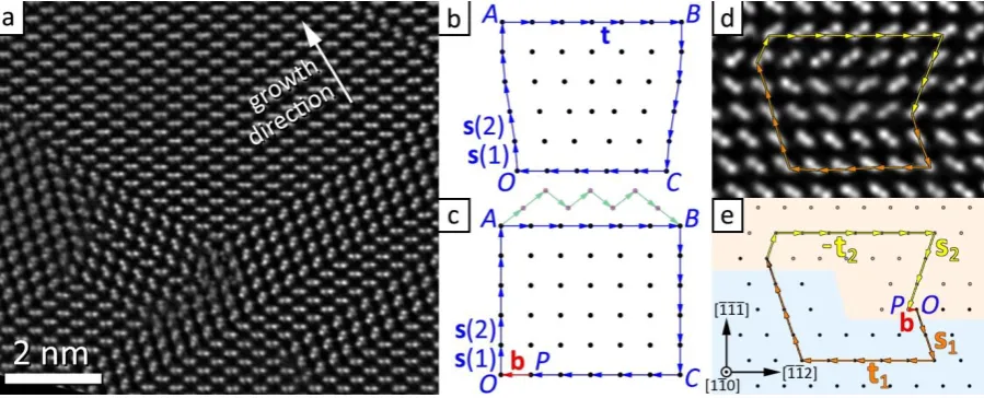
Figure 1. a) Atomic resolution ADF image of a multiply-twinned region close to the end of a GaAsP NW after droplet consumption. The Burgers vector content of such images is not readily apparent. b) Formation of a Burgers circuit OABCO using a series of vectors around a dislocation with line direction into the page. c) mapping of the Burgers circuit onto a perfect reference lattice giving OABCP and the Burgers vector b. d) and e) the procedure applied for a defect in a {111} twin boundary (here an extrinsic twinning dislocation with a step 2 ML in height). Orange vectors correspond to lattice (1) and yellow vectors to lattice (2).
Our approach to determine the Burgers vector of a dislocation is shown schematically in Figs. 1(b) and (c). On the high resolution micrograph a closed Burgers circuit is drawn,[13] (Fig. 1b) beginning
6 number of steps chosen and the choice of start point O. For example, it is perfectly acceptable to replace a section of the circuit AB with a different set of vectors that correspond to a different lattice, as long as their vector sum AB is identical (Fig. 1c). Burgers vector components perpendicular to the plane of the high-resolution image cannot be detected.
From Fig. 1(c) it is clear that, for dislocation line direction into the image, the Burgers vector b is given by the negative of the sum of the vectors that make up the circuit, i.e. for Fig. 1(b) and (c)
−𝐛 = 5𝐬 + 6𝐭 − 5𝐬 + 5𝐭 = 𝐭 (1)
Now, since this result is independent of the choice of origin O, we do not have to explicitly perform the mapping operation to determine the Burgers vector. We can simply take the vector sum of the individual vectors that make up the closed circuit in the high-resolution image, as given in Eq. (1). This is preferable by far to the alternative procedure of forming a circuit with a fixed number of vectors that is placed on the experimental (i.e. deformed) image [14], since the latter procedure cannot
easily be applied in multiply-twinned crystals or grain boundaries.
7 obtain b, all vectors must of course be written in the same reference frame. This means that vectors in one reference frame must be expressed in another, where they may not be lattice translation vectors (see Appendix section A1). When a dislocation lies in an interface, there will be two equivalent ways to describe the same dislocation, depending upon which reference frame is chosen.
These rules are applied throughout this article and are illustrated in Figs. 1(d) and (e), for a step with a height of two monolayers (2ML) in a twin boundary. Here, we have two lattices, defined by basis vectors 𝒔1and 𝐭1 and 𝒔2 and 𝐭2 respectively. The line direction is into the image, i.e. [1̅10], and the Burgers circuit may be written, starting at O,
−𝐛 = 2𝐬1+ 5𝐭1− 4𝐬1− 𝐬2− 6𝐭2+ 3𝐬2= −2𝐬1+ 2𝐬2− 𝐭2 (2)
where the first sum describes the complete circuit, and the second the components remaining once positive and negative vectors are allowed to cancel. We will use the latter, shorter form in subsequent equations. We use
𝐬1 = 1
2[101] or 1
2[011], 𝐭1= 𝐭2= 1
2[101̅] or 1
2[011̅], 𝐬2= 1
6[411] or 1
6[141]. (3)
Here, there are two possible options for 𝐬1, 𝐬2 and 𝐭1, since we cannot say whether they have a component into or out of the image. (See Appendix section A2 for more detail.) Using our principle that we should choose the sum with the smallest possible out-of-image component we obtain
−𝐛 =1
6[12̅1] or 1
6[2̅11], (4)
with a Burgers vector at 30° to the line direction and a component out of, or into, the image respectively. This Burgers vector is correct for an extrinsic twinning dislocation in a face-centred cubic (fcc) lattice. Although the dislocation can only be one of these two possibilities, it is not possible to distinguish between them from the high-resolution image since the Burgers vector component parallel to the beam cannot be determined. The dislocation core is in agreement with previous observations of 30 extrinsic partial dislocations, in e.g. CdTe and diamond. 15, 16
OBSERVED DEFECTS IN NANOWIRES
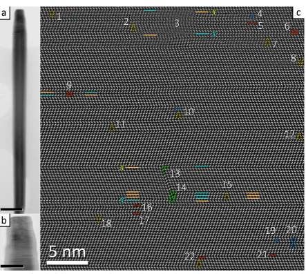
Figure 2a shows a GaAs1-xPx nanowire grown by Ga-droplet vapour-liquid-solid (VLS) growth. At the
8 temperature under As and (low) P flow. This is followed by GaAsP shell growth by vapour-solid mechanism. The end of the NW clearly contains many defects (Figs 2(b) and (c)). Can it be true that none of these defects have long-range strain fields? And if not, what kind of defects can be found in NWs?
Figure 2. a) Bright field STEM image of a Ga-droplet catalysed NW, where the droplet has been converted into GaAsP at the end of the growth. Scale bar 200nm. (b) Bright field STEM image of the top of the NW, showing highly defective material. Scale bar 100 nm. C) Atomic reslution ADF STEM image (band pass filtered) of a defective region. Different structures are highlighted with heights of 1ML (red), 2ML (blue) 3ML (orange) or multiple twinning (green). There is also a perfect dislocation at the top centre of the image. Yellow/cyan bars highlight some of the changes in dumbbell orientation of (111) planes.
9 dislocation character, (if they do not lie in a twin boundary, they are considered to be partial dislocations bounding intrinsic and extrinsic stacking faults respectively13) while those 3ML in height
[image:10.595.73.527.256.370.2]do not. There are indeed many defects with dislocation character present; of the 22 defects visible in Fig. 2(c), 11 have Burgers vectors and 11 do not. However, as will be shown below, all defects with Burgers vectors are trapped by their interaction with other defects, and are often in configurations close to those with b = 0. It is also the case that many of the defect structures seen in Fig. 2(c) would be unusual in bulk material,16 and are worth examining in more detail.
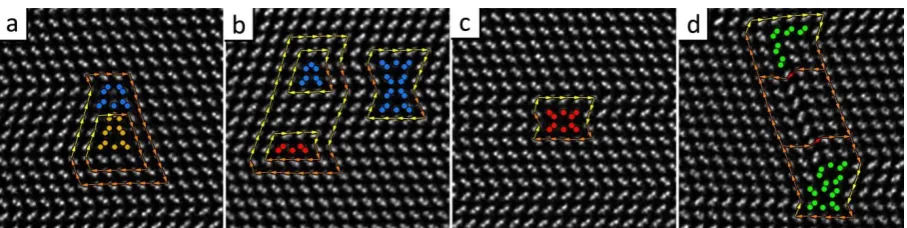
Figure 3. Burgers circuits around some of the defects in Fig. 2(c). Each image is roughly 5nm in width. a) Defect #10, the termination of a twin a 5ML in height at a (211) facet. (b) Defects #19, #20 and #21, 1ML and 2ML defects. c) Defect #9. d) Defects #13 and #14. Colour scheme for the Burgers circuit is the same as Fig. 1, with the addition of red vectors for reference frame 3.
Figure 3(a) shows defect #10, where a twin five monolayers in height terminates at a (211) facet. Two Burgers circuits are shown, one around the 3ML lower part of the structure, and a second around the complete defect. These give the respective Burgers vectors
−𝐛 = 3𝐬1− 3𝐬2+ 2𝐭1 (5a)
and
−𝐛 = 5𝐬1− 5𝐬2+ 3𝐭1. (5b)
Substituting the crystal vectors from Eq. (3) into Eq. (5a) for the 3ML lower part of the structure gives
𝐛 = 𝟎, (6a)
10 𝐛 =1
6[2̅11] or 1
6[12̅1]. (6b)
i.e. the 2ML defect is an extrinsic 30° partial dislocation (in fact, with the same core structure as Fig. 1d). Presumably, it reduces its energy slightly by being adjacent to the 3ML defect. However, the 3ML defect will act as a drag on the partial dislocation and slow its movement, acting to stabilize it inside the NW. A similar argument can be made for the 3ML +1ML defect #22.
Interestingly, the core structure of this 30° extrinsic partial in Fig. 3(a) is the same as the lower two layers of the 3ML defect, but other 30° extrinsic partial core structures can be found, as shown in Fig. 3(b). On the left in this image there is a 1ML intrinsic 30° partial dislocation (with core highlighted in red) and above it a 2ML extrinsic partial dislocation (blue). Here, the 1ML defect has the same structure as the lower layer of the 3ML defect, while the 2ML defect has the same structure as the upper two layers of the 3ML defect. Burgers circuits are shown in Fig. 3(b) for the 1ML defect #21:
−𝐛 =1
6[21̅1̅] or 1
6[1̅21̅], (7a)
which shows that it is a 30° intrinsic partial dislocation. For the 2ML defect #19: −𝐛 =16[12̅1] or 1
6[2̅11]. (7b)
i.e. a 30° extrinsic partial dislocation. The larger circuit around both gives:
−𝐛 = 𝟎 (7c)
That is, if both defects are considered together they have zero Burgers vector; they therefore form a dislocation dipole and their long-range strain fields will cancel at a sufficiently large distance. There is an attractive force between the defects that holds them in place. Defects #4 and #5 in Fig. 2(c) form a similar, even more closely spaced pair.
11 using 1ML intrinsic partial dislocations, as shown in Fig. 3(c), where an intrinsic stacking fault changes its position by one monolayer. The change in orientation of the dumbbells in the (111) planes on either side of defect #9 is highlighted by yellow and cyan bars in Fig. 2(c). Again, the Burgers circuit can be seen to sum to zero simply by inspection. Defects #9, #11 and #20 form a set of three distinct line defects, all of which have topological character similar to dislocations, but with zero Burgers vector.
The defects shown in Fig. 3(d) have an additional feature that is not present in the other defects, i.e. a stacking fault on the (111̅) plane, which is not perpendicular to the NW axis. We therefore need a third pair of vectors for this orientation:
𝐬3= 𝐬1= 1
2[101], 𝐭3= 1
6[141̅] or 1
6[411̅]. (8)
Three Burgers circuits are shown in Fig. 2(d), one around the upper defect, one around the lower defect, and joined together to form a single circuit around both. For the upper circuit
−𝐛 =1 3[110],
(9a)
Its structure shows that it is a Lomer-Cottrell lock (LCL), a result of the intersection of two intrinsic stacking faults on different {111} planes.13, 16 However, the Burgers vector is incorrect; a LCL has b =
1/6<110>. The observed Burgers vector presumably results from the reaction of a b = 1/6[110] LCL with a perfect b = 1/2[1̅1̅0] dislocation. The lower circuit gives:
−𝐛 =16[110]. (9b)
which is again a LCL, although it is unrecognisable as such due to the twins intersecting the dislocation core. The larger circuit around both gives:
−𝐛 =1
2[110] (9c)
12 driving them out of the NW. The example of Fig. 3(d) shows the utility of the Burgers circuit construction used here, since there is no single reference frame that can be used to construct a Burgers circuit, making other approaches impossible to apply. While the upper defect is recognisable as a LCL simply from its appearance, the lower defect is more complicated. Here, a 3ML twin is combined with the LCL, as highlighted by the cyan and yellow bars on Fig. 2(c). This results in a core structure that has some similarity to defect #9, combined with a 3ML (211) twin facet that has a twinned edge. Furthermore, examining (111) planes on either side of defects #13 and #14, it is seen that two (111) planes change dumbbell orientation overall, marked by cyan and yellow bars 𝑥 in Fig. 2(c).
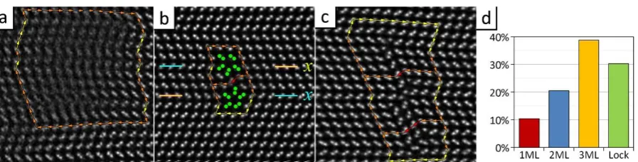
Figure 4. a) Defect #3 in Fig. 2(c), a locked crystal dislocation. (b) A pair (dipole) of Hirth locks. c) a ½[110] dislocation that has dissociated into three 1/6[110] dislocation locks. Each image is roughly 5nm in width. d) the distribution of observed defect types.
The Burgers circuit method can also be applied around a region where atom columns are imperfectly resolved, such as defect #3 at the top of Fig. 2(c). Figure 4(a) shows a circuit around the defect:
−𝐛 = −𝐬1= 1
2[101] or 1
2[011], (10)
i.e. a perfect crystal dislocation. However, the defect is not so simple; examination of the dumbbells on either side of the defect reveals changes of orientation in two (111) planes in a similar fashion to defects #13 and #14, also marked 𝑥 in Fig. 2(c). Therefore, while there is a dislocation with a non-zero Burgers vector, other defects are also present with zero net Burgers vector that are likely to lock it in place.
Other types of lock were also observed, such as that shown in Fig. 4(b). This a Hirth lock13, 16, again
13 −𝐛 =1
3[001̅], (11a)
while the lower circuit gives
−𝐛 =1
3[001], (11b)
i.e. with equal and opposite Burgers vector. This is yet another example of a defect with no net Burgers vector that changes the dumbbell orientation in a pair of planes (marked by bars 𝑥 in Fig. 4(b)). Finally, Fig. 4(c) shows a complicated set of three defects that each have different core structures and interact with stacking faults on the (111̅) plane. Burgers vector analysis shows that each of the defects has Burgers vector
−𝐛 =1
6[1̅1̅0], (12a)
which sum to
−𝐛 =1
2[1̅1̅0], (12b)
as is also found by considering the complete outer circuit. Fig. 4(c) therefore shows a crystal dislocation that is dissociated and locked in place.
14 CATHODOLUMINESCENCE
To ascertain the impact of these defects on properties, we performed cathodoluminescence (CL) imaging and spectroscopy on individual NWs (Figure 5). CL has proven to be a powerful tool to study correlations between defect structures and optical properties in e.g. GaN nanowires.17, 18The
low-phosphorous shell aids carrier confinement in the core of the NW body and allows efficient radiative recombination. A broad emission peak from the body of the NW is present, with maximum at ~690nm. A smaller peak at 627nm is ascribed to instrumental background. Fig. 5b shows a comparison between the luminescence of the tip and the body, showing that there is no detectable emission from the tip. This is consistent with the band gap closing calculated for 3ML (211) twin facets12 and expected for
[image:15.595.166.426.380.520.2]the other defects we observe due to non-radiative recombination at under-or over-coordinated atoms at their cores. The defects are clearly deleterious to NW properties.
Figure 5. a) Composite SEM and panchromatic CL image of an individual NW, showing strong luminescence from the NW body and an absence of emission from the defective tip. Scale bar 1μm b) CL spectra taken from the NW shown in (a) showing a broad luminescence peak with maximum at 687nm from the NW body and an absence of signal from the tip.
DISCUSSION AND CONCLUSIONS
15 showed that the 3ML {211} twin step facet may be expected to act as a non-radiative recombination centre, even though it has no Burgers vector. Many of the defects we describe here have similar structural components, in particular the 1ML intrinsic and 2ML extrinsic partial dislocation cores are effectively sub-units of the 3ML structure. Other, more complex structures have also been observed, with Burgers vectors corresponding to those of Lomer-Cottrell locks 1
6〈110〉 and Hirth locks 1 3〈001〉, although often they are unrecognisable as such due to the presence of twins. The bonding in the cores of these structures does not follow the tetrahedral coordination of bulk material and it is clear from the CL data that these defects are problematic recombination centres.
This study shows that line defects can exist stably within nanowires despite the common belief that they are driven out of the interior of the nanowire by surface forces. . The nanowires studied here have diameters of the order of tens of nm and of course much smaller crystallites can be produced. It seems likely that at least some of the defects seen in our material would not be stable in smaller nanowires, which would have very strong surface forces. The crystallite size at which all line defects become unstable remains to be determined. The high density of defects observed here does not occur in the major part of NWs produced by the VLS process, which have been shown to have planar growth fronts and monolayer-by-monolayer growth.7, 19 However, it is now clear that line defects with zero
Burgers vector exist and can be found in NWs. It would be prudent to minimise their density in NWs, since they could reduce the reliability of devices through processes such as recombination-enhanced dislocation climb.20 They probably originate through the loss of monolayer-by-monolayer growth,
with crystallisation occurring at multiple sites resulting in mis-registry of the crystal planes once coalescence occurs. This effect may be minimised through the use of optimised droplet consumption protocols.8, 21-23
16 accounting for ~40% of all defects in our material. We have observed two new types of line defect with zero Burgers vector, which result from the combination of a pair of intrinsic or extrinsic partial dislocations respectively. Dislocations, with long-range strain fields, are either rendered immobile through the formation of locks or form dipoles with other dislocations, with the result that the long-range strain field of the combination of defects is zero. This microstructure is unique to NWs and quite different from that seen in bulk material. CL shows that they quench luminescence. Identification and understanding of these defects is essential if they are to be eliminated by growth optimisation, allowing nanowire devices to develop into a mature technology.
AUTHOR INFORMATION
Corresponding Authors*E-mail: [email protected] *E-mail: [email protected] ORCID
Ana M. Sanchez: 0000-0002-8230-6059
Author Contributions
A.M.S. and J.A.G performed aberration corrected STEM with samples prepared by prepared by Y.Z. and H.L. R.B. determined the Burgers vector of defects. J.A.G and H.A.F determined the optical properties using cathodoluminescence. R.B. and A.M.S. wrote the paper with input from all authors. A.M.S. supervised and coordinated this piece of research. Supporting data may be obtained from http://wrap.warwick.ac.uk/ 99384
COMPETING FINANCIAL INTERESTS
The authors declare no competing financial interests
ACKNOWLEDGEMENTS
18 1. Yunyan, Z.; Jiang, W.; Martin, A.; Huiyun, L. Journal of Physics D: Applied Physics 2015, 48, (46), 463001.
2. Hannah, J. J.; Jessica, L. B.; Christopher, L. D.; Sarwat, A. B.; Michael, B. J. Semiconductor Science and Technology 2016, 31, (10), 103003.
3. Yan, R.; Gargas, D.; Yang, P. Nature Photonics 2009, 3, 569.
4. Dasgupta, N. P.; Sun, J.; Liu, C.; Brittman, S.; Andrews, S. C.; Lim, J.; Gao, H.; Yan, R.; Yang, P. Advanced Materials 2014, 26, (14), 2137-2184.
5. LaPierre, R. R.; Robson, M.; Azizur-Rahman, K. M.; Kuyanov, P. J. Phys. D-Appl. Phys. 2017, 50, (12), 10.
6. Eshelby, J. D. Journal of Applied Physics 1953, 24, (2), 176-179.
7. Jacobsson, D.; Panciera, F.; Tersoff, J.; Reuter, M. C.; Lehmann, S.; Hofmann, S.; Dick, K. A.; Ross, F. M. Nature 2016, 531, (7594), 317-+.
8. Zhang, Y.; Fonseka, H. A.; Aagesen, M.; Gott, J. A.; Sanchez, A. M.; Wu, J.; Kim, D.; Jurczak, P.; Huo, S.; Liu, H. Nano Letters 2017, 17, (8), 4946-4950.
9. Dubrovskii, V. G.; Sibirev, N. V.; Cirlin, G. E.; Tchernycheva, M.; Harmand, J. C.; Ustinov, V. M. Physical Review E 2008, 77, (3), 031606.
10. Wang, H.; Zepeda-Ruiz, L. A.; Gilmer, G. H.; Upmanyu, M. Nature Communications 2013, 4, 1956.
11. Wen, C. Y.; Tersoff, J.; Hillerich, K.; Reuter, M. C.; Park, J. H.; Kodambaka, S.; Stach, E. A.; Ross, F. M. Physical Review Letters 2011, 107, (2), 025503.
12. Sanchez, A. M.; Zhang, Y.; Tait, E. W.; Hine, N. D. M.; Liu, H.; Beanland, R. Nano Letters 2017, 17, (4), 2454-2459.
13. Hirth, J. P.; Lothe, J., Theory of Dislocations. Krieger Publishing Company: 1982.
14. Arroyo Rojas Dasilva, Y.; Kozak, R.; Erni, R.; Rossell, M. D. Ultramicroscopy 2017, 176, 11-22. 15. Lu, P.; Smith, D. J. Philosophical Magazine B 1990, 62, (4), 435-450.
16. Nabarro, F. R. N.; Duesbery, M. S., Dislocations in Solids. Elsevier Science: 2002.
17. Liu, B.; Yuan, F.; Dierre, B.; Sekiguchi, T.; Zhang, S.; Xu, Y.; Jiang, X. ACS Applied Materials & Interfaces 2014, 6, (16), 14159-14166.
18. Nogues, G.; Auzelle, T.; Hertog, M. D.; Gayral, B.; Daudin, B. Appl. Phys. Lett. 2014, 104, (10), 102102.
19. Gamalski, A. D.; Tersoff, J.; Stach, E. A. Nano Letters 2016, 16, (4), 2283-2288. 20. Ueda, O. Microelectron. Reliab. 1999, 39, (12), 1839-1855.
21. Dubrovskii, V. G., Nucleation Theory and Growth of Nanostructures. 1 ed.; Springer-Verlag Berlin Heidelberg: 2014.
22. Dastjerdi, M. H. T.; Boulanger, J. P.; Kuyanov, P.; Aagesen, M.; LaPierre, R. R. Nanotechnology 2016, 27, (47), 7.