i
i
Novel structures for
lattice-mismatched
Infrared
photodetectors
A thesis submitted in part fulfilment for the degree of
Doctor of Philosophy at the University of Lancaster
A. P. Craig (2015, revised 2016)
Supervisor: A. R. J. Marshall
ii
ii
Acknowledgements
Firstly, I would like to thank my supervisor, Dr Andrew Marshall, for his tireless support, guidance and optimism throughout the last four years. I would further like to thank Prof. Antony Krier, my deputy supervisor, for his support, and for facilitating a collaboration with the group of Prof. Sanjay Krishna at Center For High Technology materials Albuquerque, USA.
I would also like to thank our colleagues at Amethyst Research – especially Manish Jain, with whom I have worked closely throughout my PhD. Amethyst have provided additional funding and given me the opportunity to take part in world-leading research.
Credit should also be given to the departmental and support staff here at Lancaster: to Steve Holden, for arranging countless purchase requests, to Stephen Holt, who provided all manner of support for all things electronic, and to Shonah Ion, who provided safety training and support.
iii
iii
Papers published
A. P. Craig, A. R. J. Marshall, Z.-B. Tian, S. Krishna and A. Krier, “Mid-infrared InAs0.79 Sb0.21-based nBn photodetectors with Al0.9Ga0.2As0.1Sb0.9 barrier layers, and comparisons with InAs0.87Sb0.13 p-i-n diodes, both grown on GaAs using interfacial misfit arrays”, Applied Physics Letters, 103 253502 (2013).
A. P. Craig, C. J. Reyner, A. R. J. Marshall and D. L. Huffaker, “Excess noise in GaAs and
AlGaAs avalanche photodiodes with GaSb absorption regions—composite structures grown using interfacial misfit arrays”, Applied Physics Letters, 104, 213502 (2014).
A. P. Craig, A. R. J. Marshall, Z.-B. Tian and S. Krishna, “Mid-infrared InAsSb-based nBn photodetectors with AlGaAsSb barrier layers – grown on GaAs, using an interfacial misfit array, and on native GaSb”, Infrared Physics and Technology, 67, p210 (2014).
A. P. Craig, M. Jain, G. Wicks, T. Golding, K. Hossain, K. McEwan, C. Howle, B. Percy and A. R. J. Marshall, “Short-wave infrared barriode detectors using InGaAsSb absorption material lattice matched to GaSb”, Applied Physics Letters, 106, 201103 (2015).
A. P. Craig, M. D. Thompson, Z.-B. Tian, S. Krishna, A. Krier and A. R. J. Marshall, “InAsSb-based nBn photodetectors: lattice mismatched growth on GaAs and low-frequency noise performance.” Semiconductor Science and Technology, 30, 105011 (2015).
Papers under review
A. P. Craig, P. J. Carrington, H. Liu and A. R. J. Marshall, “Heteroepitaxial techniques for the
growth of 6.1 Å III-V materials on GaAs and Si – a comparison of GaSb/GaAs epitaxy and GaSb/Si epitaxy.” Journal of Crystal Growth (2015).
Oral presentations at conferences
iv
iv
A. P. Craig, A. R. J. Marshall, Z.-B. Tian and S. Krishna, “Mid-infrared InAs0.91Sb0.09-based
nBn photodetectors with Al0.9Ga0.1As0.08Sb0.92 barrier layers – grown on GaAs, using an Interfacial Misfit Array, and on native GaSb”,
- Quantum Structured Infrared Photodetector (QSIP), Santa-Fe, N.M. USA (2014). - UK Semiconductors, Sheffield (2014).
- Mid-IR Optoelectronics: Materials and Devices (MIOMD), Montpellier, France (2014).
A. R. J. Marshall, A. P. Craig, C. J. Reyner and D. L. Huffaker, “GaAs and AlGaAs APDs with GaSb absorption regions in a separate absorption and multiplication structure using a hetero-lattice interface”,
- Quantum Structured Infrared Photodetector (QSIP), Santa-Fe, N. M. USA (2014). - UK Semiconductors, Sheffield (2014).
A. P. Craig and A. R. J. Marshall, “InAs0.91Sb0.09-based nBn photodetectors: the influence of absorption layer doping and 1/f noise performance”, UK Semiconductors, Sheffield (2015).
v
v
Table of contents
(1) Introduction... 1-6 (2) Theory…... 7-31
2.i Dark Current Mechanisms………..……….. 7
2.ii Capacitance-Voltage Measurements... 12
2.iii Avalanche Photodiodes (APDs) and Impact Ionisation……. 14
2.iv Noise... 15
2.v Limitations of the Local Model of Impact Ionisation……….. 17
2.vi Figures of merit………..………. 18
2.vii Bandstructure modelling………..………. 20
2.viii Device structures………..……… 24
2.ix Critical thickness modelling………..………...……….. 28
(3) Literature review……… 32-61 3.i Interfacial misfit (IMF) arrays for lattice mismatched growth……….... 32
3.ii nBn detectors for long wavelength detectors with low dark currents and noise……….. 43
3.iii Comparison with HgCdTe performance levels using Rule 07.……… 52
3.iv Avalanche photodiodes for high sensitivities in long wavelength applications………. 53
(4) Experimental methods and modelling……….. 62-85 4.i Molecular beam epitaxy…..………. 62
4.ii Hall effect measurement…………..……… 68
4.iii X-ray diffraction (XRD)…………..………..………… 70
4.iv Device processing………..……...………….. 72
4.v Characterisation techniques………..………... 77
4.vi Modelling…..………...…………... 80
(5) Results and Discussion I – IMF Arrays……… 86-102 5.i Growth of GaSb IMF p-i-n diodes…………..………. 86
5.ii XRD and transmission electron microscopy (TEM) characterisation of GaSb IMF p-i-n diodes……… 88
5.iii Electrical and optoelectronic characterisation of GaSb IMF p-i-n diodes……….. 94
5.iv Discussion………..………...….. 98
(6) Results and Discussion II – nBn detectors for Mid-Infrared applications………... 103-128 6.i Growth of nBn detector samples……..……… 103
6.ii Characterisation of nBn detector samples…………..……….. 107
6.iii The effects of absorption layer doping upon nBn detector performance………... 118
6.iv Longer-wavelength nBn detector sample……...…..……….. 120
vi
vi
6.vi Discussion………. 124
(7) Results and Discussion III – Extended wavelength APDs………. 129-145 7.i Growth of extended wavelength APDs………... 129
7.ii IV and CV characterisation of extended wavelength APDs.. 130
7.iii Determination of multiplication……….….……….. 133
7.iv Excess noise measurement……..……….. 137
7.v Excess noise results………..………. 139
7.vi Discussion………...………... 143
(8) Conclusions and further work……… 146
Appendix I – Constants for bandstructure modelling……… 151
vii
vii
List of common symbols
μ Absorption coefficient
A Area
Eg Bandgap
Δf Bandwidth
k Boltzmann Constant
C Capacitance
T0 Characteristic Temperature
hc Critical thickness
J Current density
IV Current voltage measurement
JV Current-density voltage measurement
w Depleted volume width
ϵr Dielectric constant (relative)
ξ Electric field
q Elementary charge
F Excess Noise factor
Ef Fermi Energy
M Gain
ni Intrinsic carrier concentration
α Ionisation coefficient for electrons
β Ionisation coefficient for holes
keff Ionisation coefficient ratio
Eth Ionisation threshold energy
a0 Lattice Constant
I2 Noise current
ϵ0 Permittivity of free space
h Planck Constant
I0 Primary photocurrent
η Quantum Efficiency
viii
viii
RdA Resistance-area product (dynamic)
R0A Resistance-area product (zero-bias)
D∗ Specific Detectivity
c Speed of light in a vacuum
Δ0 Spin orbit split-off energy
ϵ Strain
T Temperature (in Kelvin)
ix
ix
Abstract
Using the interfacial misfit (IMF) array growth mode, GaSb p-i-n diodes were grown on Si and GaAs lattice-mismatched substrates by molecular beam epitaxy (MBE) under optimised growth conditions. For the sample grown on Si, an AlSb nucleation layer was used to reduce the occurrence of twinning defects. In addition to the samples grown on mismatched substr-ates, an equivalent structure was further grown on a native GaSb substrate, for comparison. X-ray diffraction (XRD) was used to demonstrate that the layers were fully relaxed, and tran-smission electron microscopy (TEM) imaging showed arrays of 90° misfit dislocations with measured periodicities in agreement with atomistic modelling. However, after processing, device dark current densities of 0.9 𝐴𝑐𝑚−2 and 0.18 𝐴𝑐𝑚−2 were recorded for the sample grown on Si and the sample grown on GaAs, respectively, at -1.0 V and 300 K. These were compared to the sample grown on native GaSb, which had a dark current density of
0.01 𝐴𝑐𝑚−2 under the same conditions. Furthermore, TEM analysis revealed relatively high
threading dislocation densities (TDDs) of ~108 𝑐𝑚−2. It was proposed that not all the
interf-acial strain could be accommodated by the IMF arrays, since the array periods (9:8 for AlSb/Si and 13:14 for GaSb/GaAs) were not in exact agreement with ratio of the lattice con-stants (of AlSb to Si and GaSb to GaAs), i.e. a population of 60° misfit dislocations was still formed.
It was therefore decided to investigate the use of nBn detector structures as lattice mismat-ched photodetectors. Using a design based on an InAsSb bulk-material absorber, a compar-ison was again drawn between two samples, one grown on mismatched GaAs and a second grown on native GaSb. This time, device dark current densities were found to be relatively
similar when comparing the two samples (1.6 × 10⁻⁵ 𝐴𝑐𝑚−2 vs 3 × 10⁻⁶ 𝐴𝑐𝑚−2 at 200 K).
𝐷∗ performance figures were also found to be within one order of magnitude (1.5 ×
pe-x
x
rformance was exhibited at all temperatures tested, so that the effects of Shockley Read Hall (SRH) generation were established to be absent (or at least much less significant). It was also found that absorption layer doping of around ~4 × 10¹⁷𝑐𝑚−3 was necessary to ensure
diffu-sion limited performance for the sample grown on GaAs and that, with this modification, diff-usion limited performance was achieved even for a sample with a highly lattice-mismatched absorption layer (with higher Sb content and longer cut-off wavelength).
While nBn detector structures offer very low dark currents, it will sometimes be necessary to have a detector which is sensitive to very weak signals. In telecoms applications, avalanche photodiode (APD) structures are often used as receivers for long-haul fibre optic systems. However, relatively few avalanche photodiode designs exist for wavelengths beyond 1.55 μm. Two novel separate-absorption-and-multiplication (SAM) APD structures were therefore demonstrated based on the IMF growth mode. In particular, by transitioning the lattice from 5.65 Å to 6.09 Å, it was possible to combine GaSb absorption layers with GaAs and (for improved noise performance) Al0.8Ga0.2As multiplication layers. Multiplication profiles were
established using capacitance voltage modelling (together with ionisation coefficients from the literature) and excess noise measurements were then carried out. Through the presence of 1.55 μm photocurrent, it was confirmed that absorption took place in the GaSb regions, with transport to the p-n junction (in the multiplication region) taking place by diffusion. Through measurements showing 0.2 < 𝑘𝑒𝑓𝑓 < 0.4 and 0.1 < 𝑘𝑒𝑓𝑓 < 0.2 it was confirmed that
mul-tiplication of the photocurrent took place in the GaAs and Al0.8Ga0.2As layers. Extension of the
1. Introduction - 1
1
(1) Introduction
At present, commercially available sensors and focal plane arrays (FPAs) working in the
mid-wave infrared (MWIR) spectral range (3 – 5 μm) are predominantly based on HgCdTe alloy materials.1 InAs and InSb detectors are also available commercially, but the latter always require cooling to 77 K for operation. However, devices based on quantum structured III-V
designs, such as quantum well infrared photodetectors (QWIPs) and quantum dot infrared photodetectors (QDIPs) have been developed as alternatives.1 Table 1 compares the specific
detectivity (D∗), cut-off wavelength and operating temperature for commercial HgCdTe, InAs
and InSb detectors from Teledyne Judson and Vigo S.A., as well as for QWIP detectors from Jet Propulsion Laboratory (JPL). Ultimately, HgCdTe has remained the “market leader”, being
employed almost exclusively by military end-users,2 as well as commercial users. While thermoelectrically cooled HgCdTe sensors are widely available, HgCdTe inherently suffers from certain disadvantages, notably fragility due to the weak HgTe bond strength, poor
compo-sitional uniformity and the additional cost associated with these factors. There is therefore an identified need for alternative detector designs which can be operated under thermoelectric
cooling (200 – 240 K) and grown and processed more cheaply than HgCdTe. As commented earlier, novel structures based on III-V materials are promising candidates for these purposes. The primary application for infrared sensors is thermal imaging, e.g. famously for “hotspot” in
test match cricket – where small changes in temperature are mapped to show contact between bat and ball – or for target acquisition in defence applications.2 Further applications include the sensing of toxic or pollutant gasses.3 Such gasses often have absorption lines in the MWIR,
e.g. methane (3.3 μm), CO2 (4.2 μm), and CO (4.6 μm), permitting gas detection systems based on spectral “fingerprints”. New detectors are required to complement recently-developed
1. Introduction - 2
2 Technology Operating
temperature
Cut-off wavelength
D∗ Reference
InSb 77 K 5.5 μm 9 × 10¹⁰cmHz1/2 W−1 [5] InAs 233 K 3.5 μm 3 × 10¹⁰cmHz1/2 W−1 [6] HgCdTe 230 K 3.5 μm 6 × 10¹⁰cmHz1/2 W−1 [7] QWIP 95 K 5.5 μm 5 × 10¹¹cmHz1/2 W−1 [8]
QWIP 77 K 9 μm 9 × 10¹⁰cmHz1/2 W−1 [8]
Table 1: Examples of some mid-wave infrared detector products available commercially.
gas sensing, i.e. subtle differences in the incident photon flux must be resolved.
At the same time, designs for heterostructures based on III-V materials are usually constrained through the requirement for lattice matching to a “native” substrate. The manufacture of GaAs
and InP substrates has matured so that larger areas (>3” diameter) and semi-insulating varieties are available.9 However, Sb-bearing compounds, e.g. InAsSb, are typically required for
sensi-tivity in the MWIR spectral range – that is to say their bandgap is small enough that photons with wavelengths between 3 - 5 μm can be absorbed by bulk material. Bulk InAsSb material is typically grown lattice matched to GaSb – lattice constant 6.1 Å – and cannot be grown lattice
matched to GaAs – lattice constant 5.65 Å. (While QWIPs or QDIPs detectors operating in the MWIR can be grown on GaAs, devices based on bulk materials are simpler to grow and
typ-ically offer higher responsivities). However, GaSb substrates have a cost around six times greater9 than GaAs substrates and are not available in the largest areas or in semi-insulating varieties. Clearly therefore, it would be beneficial to grow MWIR bulk materials on GaAs
substrates. However, the lattice mismatch between GaSb and GaAs is large (7.78%) and the result of this is the inevitable occurrence of threading dislocations which propagate into the
electrically active overlayers. These tend to impact device performance significantly. In recent years, workers at the Department of Electrical Engineering at UCLA have claimed progress in the direct growth of GaSb on GaAs.10 Through the interfacial misfit (IMF) array growth
supp-1. Introduction - 3
3
orting high quality device layers with low (<106 cm-2) threading dislocation densities (TDDs)
have been reprted.11
In this work, IMF arrays were used to grow 6.1 Å-lattice-constant materials on GaAs substr-ates without the need for a thick metamorphic buffer (250 – 500 nm buffer thickness). The first key objective of this work was to verify the quality of the material grown, in terms of the TDD, and in terms of the effects of this TDD on device performance.
In order to investigate the material quality achievable under IMF growth, simple p-i-n diodes were grown in Section (5). These were based both on GaSb/GaAs and GaSb/AlSb/Si mis-matched epitaxy. A lattice mis-matched structure (on GaSb) was also grown for comparison.
Cross-sectional transmission electron microscopy (TEM) was used to characterise the material quality in each case. Electrical characterisation of processed devices was also carried out. It was found
that defect density levels were significantly greater than those quoted by ref [11]. Electrical performance was also compromised, with 300 K dark current densities increasing (by compar-son with the sample on GaSb) by factors of ~15 and ~80, for the GaSb/GaAs case and for the
GaSb/Si case, respectively. Nevertheless, arrays of pure-edge dislocations (i.e. IMF arrays) were clearly visible in TEM imaging. In accordance with the literature, the array periodicities
were further noted to be in good agreement with the ratio of the lattice constants of the epilayer and substrate materials. Full relaxation of the GaSb overlayers was also confirmed through XRD Bragg scans.
1. Introduction - 4
4
nBn detector structures aim to exploit the absorption properties of a narrow-bandgap material, but at the same time achieve the dark current behaviour associated with diffusion currents, rather than Shockley Read Hall (SRH) or surface currents. nBn detectors were grown on both GaAs substrates (via an IMF array) and on native GaSb substrates in Section (6). It was
theref-ore possible to assess the impact of the choice of a mismatched substrate on the final detector performance, and in particular to determine whether SRH and surface currents – which were
found to be troublesome for the case of GaSb p-i-n devices – could be suppressed. As will be seen in the following chapters, a synergy was found to exist between the IMF growth mode and the nBn detector design, so that only moderate changes in the dark currents (around a factor
of 5 at 200 K) occurred as a result of the choice of a mismatched substrate. Furthermore, surface leakage and SRH currents were found to be almost entirely absent (for device diameters
between 50 – 800 μm). The potential for FPAs operating with thermoelectric cooling based on these structures was highlighted through specific detectivity calculations and noise
measure-ments. Specific detectivity was found to be greater than 1010 cmHz1/2W−1 at 200 K for
dev-ices grown on both GaAs and GaSb, with cut-off wavelengths of ~3.5 μm measured at the same temperature.
In the final part of this work, IMF arrays were exploited to create separate-absorption-and-multiplication avalanche photodiodes (SAM-APDs). These were based upon previously-impo-ssible GaSb/GaAs and GaSb/GaAs/AlGaAs heterostructures. The key objective of this section was to determine whether such structures still exhibited the excess noise characteristics of the wide bandgap regions, whilst at the same time being photosensitive at 1.55 μm.
While nBn detectors were investigated to determine their suitability for 2D arrays, sometimes
there will be a need for a detector with higher sensitivity, i.e. for applications where very low photon fluxes need to be measured. In Section (7), SAM-APD structures based on IMF
1. Introduction - 5
5
results from a proprietary random path length model with full field dependence. It was found
that the excess noise behaviours exhibited were consistent with multiplication occurring in the wide bandgap material, i.e. that effects due to multiplication in the absorption layers or at the IMF interface were absent, whilst the devices were also photosensitive at 1.55 μm. Gains in
excess of 103 were established for the sample with an AlGaAs multiplication region. These designs could be extended to incorporate absorption layers consisting of other materials lattice
matched to GaSb (e.g. InAsSb or InGaAsSb), allowing operation beyond 1.7 μm. Single-pho-ton devices would also be possible, by using a GaAs multiplication region.
1. Introduction - 6
6
References
[1] A. Rogalski, J. Antoszewski and L. Faraone, J. Appl. Phys. 105, 091101 (2009)
[2] I. M. Baker, S. S. Duncan and J. W. Copley, in Proc. SPIE 5406, 133 (2004).
[3] A. Krier, M. Yin, V. Smirnov, P. Batty, P. J. Carrington, V. Solovev, and V. Sherstnev,
Phys. Stat. Sol. (a) 205, 1, 129–143 (2008).
[4] G. R. Nash, S. J. B. Przeslak, S. J. Smith, G. de Valicourt, A. D. Andreev, P. J.
Carrington, M. Yin, A. Krier, S. D. Coomber, L. Buckle, M. T. Emeny, and T. Ashley, Appl.
Phys. Lett. 94 091111 (2009).
[5] “Indium Antimonide detectors”, Teledyne Judson Technologies (March 2003).
[6] “Indium Arsenide detectors”, Teledyne Judson Technologies (March 2003).
[7] “PV-2TE Series 2 – 12 µm IR Photovoltaic Detectors Thermoelectrically Cooled”, VIGO
System S.A. (2015).
[8] S. D. Gunapala, S. V. Bandara, J. K. Liu, C. J. Hill, S. B. Rafol, J. M. Mumolo, J. T. Trinh, M. Z. Tidrow and P. D. LeVan, Semicond. Sci. Technol. 20, 473 (2005).
[9] web page http://www.wafertech.co.uk/products
[10] S. H. Huang, G. Balakrishnan, A. Khoshakhlagh, A. Jallipalli, L. R. Dawson, and D. L. Huffaker, Appl. Phys. Lett. 88, 131911 (2006).
2. Background Theory - 7
7
(2) Background Theory
Essential concepts in the design and characterisation of infrared photodetectors are covered in this section to provide a basis for understanding the results presented in sections 5-7. These include carrier generation/dark current mechanisms, electrostatic behaviour in p-n junctions and the impact ionisation process (as occurring in avalanche photodiodes). Figu-res-of-merit and bandstructure and critical thickness modelling are also treated.
i) Dark current Mechanisms
Dark currents are defined as currents that flow in a photodiode without illumination. These usually depend on the applied bias. All photodiodes suffer from dark currents to some extent, and their reduction is the focus of much effort – whether through choice of materials,
heteros-tructure design, passivation techniques, or other avenues. By minimising the dark currents of a detector for a given signal level, the signal to noise ratio is maximised. Dark currents can occur via various mechanisms.
CHCC (Conduction-Hole-Conduction-Conduction) Auger generation occurs via the collision of a highly energetic conduction band electron with a second electron residing in the valence
band. The collision results in the excitation of the valence band electron into the conduction band, with a mobile hole left behind. The process is illustrated in Figure 2.1. The CHCC Auger
process is analogous to the impact ionisation process (which will be treated later in this section) but occurs even in the absence of electric field (at a lower rate). The CHCC process is known to dominate (over the other Auger processes) in direct-bandgap n-type semiconductors.1 Carriers generated in the neutral regions of a photodetector via the CHCC Auger process (or the CHLH or CHSH processes for holes) diffuse into the electric field, where they undergo
2. Background Theory - 8
8
Figure 2.1: CHCC Auger process illustrated in an E-k diagram. C.B., H.H., L.H. and S.O. indicate the conduction band, heavy hole band, light hole band and the spin orbit split-off band, respectively.
dependent, via a dependence on the square of the intrinsic carrier concentration, ni2, itself
depending exponentially on the ratio of the full bandgap to kT,2
Jdiff,p= q√Dτp
p
ni2 Nd= q√
Dp
τp 1
NdNcNvexp (− Eg
kT) (2.1)
where q is the elementary charge, Dp is the hole diffusion coefficient, τp is the minority
carr-ier lifetime, Nd is the donor concentration on the n-type side of the junction, Nc and Nv are the
density of states for the conduction and valence bands, respectively, T is temperature, k is the
Boltzmann Constant, and Egis the bandgap. The above expression refers to the diffusion
current due to minority carrier holes diffusing into the electric field from the n-type neutral region. An equivalent expression for electrons diffusing from an p-type neutral region, i.e.
[image:18.595.72.343.102.323.2]2. Background Theory - 9
9
and the acceptor level in the p-type region. One term or the other will dominate for p-n
junct-ions with asymmetric doping. For p-i-n diodes with an n-type intrinsic region, e.g. unintentio-nally doped InAs(Sb), diffusion currents result from holes diffusing from the (low n-type) intrinsic region into the field region or electrons diffusing from the p-type neutral region. In order to obtain to determine whether the diffusion mechanism is the dominant source of dark current in a particular device, it is common to plot the dark current density as a function of
inverse temperature, and then to use a fitting to the following formula to determine the
activation energy, Ea
Jdiff ∝ ni2 ∝ T3exp (−Ea
kT) (2.2)
which is a reduced form of Equation 2.1, in which the temperature dependence of NcNv is
assumed to be proportional to T3. If this energy is equal to the full, low temperature bandgap of the neutral-region semiconductor, diffusion currents are expected to be dominant.
Trap states occur due native defects or threading dislocations in the crystal lattice. These can result in generation-recombination (G-R) currents.3 Trap states contain either an electron (when
occupied) or a hole (when vacant). Shockley Read Hall (SRH) currents occur when electrons move via a trap state located within the bandgap from the valence band to the conduction band. The efficiency of the SRH process is energetically favoured for trap states lying close to the
middle of the bandgap. For this reason, the SRH process is also maximised when the Fermi level lies close to the middle of the bandgap, i.e. for intrinsic layers. On the other hand, extrinsic
doping pins the Fermi level close to the band edge, so that SRH genera-tion is suppressed in the neutral regions. The process can be encouraged by the presence of electric field, though it may still occur for zero field. SRH currents dominate below a certain temperature, referred to
as T0, which is a function of the material type and quality, among other factors. The rate at
2. Background Theory - 10
10
U = − [ σpσnvthNt
σnexp(Et−EikT )+σpexp(Ei−EtkT )
] ni = − ni
τeff (2.3)
where σp and σn are the hole and electron capture cross-sections, respectively, Nt is the
den-sity of traps, vth = √3kT/m∗ is the average thermal velocity for carriers where m∗ is
effect-tive mass, Et the trap energy level and Ei is the intrinsic Fermi level. τeff is thus defined as the
effective lifetime. The increased efficiency of the SRH process for traps with energies close to
the Fermi level can be shown by varying Ei− Et in Equation 2.3. The resulting cur-rent density due to SRH generation is then given by2
JSRH= ∫ q|U|
W
0 dx = q|U|W =
qniW
τeff (2.4)
where w is the width of the electric field region. Under the SRH dark current limited regime,
the magnitude of the dark current density is therefore directly proportional to the intrinsic
carrier concentration, so that Equation 2.4 can be rewritten as
JSRH=
qW
τeff√NcNvexp (−
Eg
2kT) (2.5)
where, once again, the temperature dependence of the density of states can again be
approx-imated to be proportional to T3 yielding the following expression for fitting.
JSRH ∝ ni ∝ T3/2 exp (
−Eg
2kT) (2.6)
Figure 2.2 shows the relative magnitude of the diffusion and SRH components of the dark current density as modelled for an InAs p-i-n diode (calculated using Equations 2.1 - 2.6). Approximate values Nc = 8.7 × 1016 cm−3 and N
v = 6.6 × 1018 cm−3, Dp= 13 cm2s−1, Dn = 1000 cm2s−1, τ
n = 3 × 10⁻⁸ s and τp = 3 × 10⁻⁶ s were taken from [4]. The
2. Background Theory - 11
11
Figure 2.2: Modelled temperature dependence of the diffusion and SRH dark current contr-ibutions for an InAs p-i-n diode.
the depletion region was assumed to be 1 μm (corresponding to -0.2 V applied bias). It can be
seen that T0 ≈ 225 K. For the case of an elevated trap density, as would be expected for
lattice-mismatched growth, JSRH, which is proportional to the trap density, would be incr-eased
further. In addition, surface leakage currents need to be considered.
Surface leakage currents are often a significant problem when designing infrared photodetec-tors. A surface inversion layer is a thin region at the surface of a semiconductor with the
opp-osite majority carrier type to the bulk. These can occur due to dangling bonds.5 Surface inversion layers can act as a shunt resistance bypassing the bulk junction. n-type surface inversion layers can occur in p-InAs(Sb) layers in particular, and these result in a conducting channel. Surface leakage currents are approximately temperature insensitive and generally result in Arrhenius plots exhibiting small activation energies. Passivation using dielectrics, e.g.
[image:21.595.77.414.73.337.2]2. Background Theory - 12
12
magnitude.5 Smaller devices are more susceptible to surface leakage effects, due to incre-ased
perimeter to area ratio. In order to determine whether processed devices are surface current limited (or bulk limited), it is useful to plot the current density for a series of mesa areas. Area scaling of the dark currents indicates that surface leakage currents are less significant, whereas
scaling with the device perimeter indicates that surface leakage currents are dominant.
ii) Capacitance-voltage measurements
When two semiconductor layers with opposite doping types meet, a p-n junction is formed. p-n junctions in semiconductor materials result in opposing drift and diffusion processes taking place. In a p-i-n diode, as illustrated in Figure 2.3, majority carriers from the p-type and n-type
neutral regions diffuse into the intrinsic layer (where the carrier population is low) and recombine with each other. This leads to an imbalance of charge due to the ionised dopant
atoms, which are immobile and remain in the neutral regions. The charge imbalance creates an electric field, resulting in a drift current which opposes the diffusion current. In the initial state, the diffusion process is stronger than the drift process and, as more carriers recombine, a space
charge region (SCR) forms, devoid of mobile carriers. The electric field remains after the two processes have reached equilibrium, forming a built-in potential. The SCR, together with the
p-type and n-type neutral regions are analogous to a parallel plate capacitor. The capacitance is given by C = ϵ0ϵrA/w, where ϵ0 and ϵr are the permittivity of free space and the relative
permittivity (of the semiconductor), respectively, A is the junction area and w the width of the
space charge region. In fact, the SCR does not begin and termi-nate abruptly, since the diffusion profile of carriers has a “rounded” profile, however it is common to use the “full-depletion approximation”.6 This effectively considers that the SCR has a definite width, given under the
2. Background Theory - 13
[image:23.595.78.412.75.319.2]13
Figure 2.3: Modelled carrier populations, as a function of position, in a GaSb p-i-n diode (with Te compensation doped intrinsic region) under -5.0 V bias.
quantum efficiency is generally dependent on the depletion width (i.e. the width of the SCR), since photogenerated carriers in the neutral regions must diffuse to the SCR for current to flow,
and since the electron-hole pairs generated within the SCR are separated with the greatest efficiency. Knowledge of the depletion behaviour, as a function of bias, is therefore essential when designing photodiodes, and becomes paramount when designing more comp-licated
heterostructures, e.g. SAM-APDs, where the electric field profile is of crucial import-ance. The SCR is more commonly known simply as “the depletion region” and will be refe-rred to as
such from here on.
Capacitance is typically measured using an LCR meter, e.g. the Agilent E4980A. The LCR meter measures the complex impedance of the device under test (DUT) for changing DC bias
voltage (using an AC test signal) before internally calculating the other impedance param-eters (resistance, reactance, conductance, susceptance, capacitance and inductance) via
2. Background Theory - 14
14
iii) Avalanche Photodiodes (APDs) and Impact Ionisation
Carriers moving within the depletion region of an avalanche photodiode (APD) can sometim-es gain sufficient energy from the electric field to generate additional carriers by impact
ion-isation. In the impact ionisation process, electrons in the valence band are promoted to the conduction band by energetic primary carriers, leaving behind mobile holes. In this way, add-itional electron-hole pairs are generated.8 Each additional carrier generated can be accelerated
by the field in the same way, and further electron hole pairs generated. In this way, carrier multiplication takes place. Figure 2.4 shows a current-voltage (IV) for an AlGaAs avalanche photodiode from Section (7). The steep rise in the current for bias conditions >10 V is due to
the impact ionisation process, with an avalanche breakdown (i.e. an infinite multiplication condition) occurring at -11.25 V (though in practice the total current is limited by the contact
resistance). The probability of ionisation is described by material-specific ionisation
coeffi-cients, which are functions of the electric field, ξ. Electrons and holes have separate
coeffic-ients, α(ξ) and β(ξ), respectively. These have dimensions of cm−1 and 1/α and 1/β are the
mean ionisation path lengths. The impact ionisation process can be exploited by APDs to amplify weak signals, i.e. to produce gain. The gain, or multiplication, is equal to the total photocurrent divided by the primary photocurrent (i.e. the photocurrent without
multipli-cation). It should be noted that the multiplication process amplifies not only the photogen-erated signal, but also the dark currents. There is also an additional noise contribution, the “excess noise”, resulting from the stochastic nature of the impact ionisation process, although
much effort goes into reducing this.9 However, if the overall signal to noise ratio is limited by noise in the external circuit (e.g. thermal noise in an external amplifier), the use of an APD
2. Background Theory - 15
15
Figure 2.4: IV characteristics of an APD device, with breakdown occurring at -11.25 V.
iv) Noise
Electronic noise presents itself as random fluctuations in an electrical signal, and can result from various mechanisms. In photodetectors, these include the absorption of background rad-iation, as well as processes intrinsic to the device, such as the thermal agitation of carriers and
the stochastic nature of the flow of individual electrons.
Thermal agitation of carriers results in thermal or “Johnson” noise.10 Thermal noise cannot be
eliminated (other than at absolute zero) but reduces with temperature. The mean square value for the associated noise current is given by,
Ithermal2 = 4kTΔf/R (2.7)
where R is the resistance of the device, T is temperature and ∆f is the measurement
[image:25.595.92.415.75.333.2]2. Background Theory - 16
16
Shot noise results from the discrete nature of electronic charge, which leads to the flow of current consisting of individual charges arriving at a given point in the circuit over time acco-rding to the Poisson Distribution.8 Shot noise is also approximately frequency independent. The mean squared shot noise current is generally taken to be
In2 = 2qI̅Δf (2.8)
where q is the elementary charge, I̅ is the mean DC current. However, the mean DC current
may differ from the total current flowing in the device, e.g. drift and diffusion currents still flow for zero bias, and so Shot noise is still present, despite zero total DC current flowing. Shot
noise is temperature independent, though the flow of dark currents will vary with temp-erature, affecting the total shot noise current.
1/f noise is, as its name suggests, a type of noise with a magnitude with inverse frequency dependence. 1/f noise can occur due to traps at surfaces or heterointerfaces. When these traps are occupied, the electron and hole mobilities are locally modulated by the trapped charge, so
that the trapping/detrapping process affect the total flow of current in the device.11 1/f noise is characterised by a “knee frequency” at which the spectral noise density of the 1/f component
is equal to that of that of the white noise (as measured at higher frequencies). Below the noise knee frequency the 1/f component dominates. The trapping/detrapping time constants are red-uced at lower temperatures, affecting the modulation and typically reducing the knee
frequ-ency.
Excess noise occurs due to the statistical nature of the impact ionisation process, as noted in the previous section. For the case that one of the ionisation coefficients (α or β) is zero,
exce-ss noise is eliminated, and gain simply increases exponentially with increasing electric field. In this case, no avalanche breakdown occurs and there is no limitation on bandwidth.8
2. Background Theory - 17
17
characteristic. This can greatly amplify any initial fluctuations in current flow and lead to
avalanche breakdown (i.e. infinite multiplication). Tager [1964] found that, for the condition
that α = β, the noise measured is greater than that for the condition where β = 0 by a factor
equal to the multiplication, M.8 McIntyre developed this relation idea to allow for arbitrary
values ratios of keff= β/α and found that, for low frequencies12
F = keffM + (1 − keff) (2 − 1
M) (2.9)
where F is the excess noise factor, so that the total noise current density, In2 is given by
In2 = 2qI
oMFΔf (2.10)
where q is the elementary charge, I0 is the primary photocurrent (i.e. the photocurrent for unity
gain) and Δf is the measurement bandwidth. McIntyre’s work is predicated on the “local model” of impact ionisation, which will be explored in the next section.
v) Limitations of the Local Model of impact ionisation
In practice, carriers accelerated by an electric field cannot initiate ionisation events until they
attain the ionisation threshold energy, Eth.13 In doing so they undergo a certain displacement,
referred to as the “dead space” which, in the ballistic approximation, is given by
d = Eth/qξ (2.11)
where ξ is the electric field. The effects of dead space are particularly pronounced at high
electric fields, where the mean ionisation path length (which is just the inverse of the partic-ular ionisation coefficient, 1/α or 1/β) is short. For high electric fields, the dead space can
become a significant fraction of the ionisation path length. The effect of the dead space can be
2. Background Theory - 18
18
fields and/or in thick devices. However, it is possible to model multiplication and excess noise
taking dead space into account. This is generally achieved using a random path length (RPL) model, or recurrence equations.14 In this work, the RPL approach will be used, with details to follow in the experimental section. The ballistic approximation considers that carriers are freely accelerated by the electric field and that no scattering occurs. As taken into account by analytical band Monte Carlo models, e.g. [15], scattering can have a significant effect on the
fitted ionisation threshold energy, in other words the threshold energy fitted in a hard-threshold model (e.g. an RPL model) is always larger than that fitted in analytical band Monte Carlo.
vi) Figures of Merit
Certain figures of merit are commonly used to provide an indication of the performance of a particular device with respect to those found elsewhere, e.g. in the literature. Those employed
most commonly in this work are outlined as follows.
Quantum efficiency is defined as the fraction of photogenerated electrons reaching the exter-nal circuit to the number of photons which arrive at the detector’s surface. The number of
ph-otons per second, or photon flux, arriving at the detector, ϕ, can be calculated, in units of s−1
using the Planck Relation
ϕ =Pλ
hc (2.12)
where P is the optical power, λ is the wavelength of the source, h is the Planck constant and c
is the speed of light. The quantum efficiency, η, is found by dividing the photocurrent, Iph, by
the product of the photon flux with the elementary charge, qϕ.
The responsivity, R, of a detector is defined as the current generated per unit optical power
incident on the detector surface, usually expressed in units of AW−1. The responsivity is closely
2. Background Theory - 19
19
R = ηqλ
hc (2.13)
It can be seen that the responsivity has an additional dependence on λ. This has implications
for the D∗ figure of merit, which can be calculated from R when the dark current density, temperature and dynamic resistance area product are known. The effect of this dependence is
that the value of D∗ measured increases as a function of the wavelength of the incident
radi-ation (due to an increased photon flux per unit power of applied radiradi-ation).
The dynamic resistance-area product, RdAd, describes the dark currents of a detector
norm-alised to the area of the device. Larger values indicate lower dark current densities. RdAd can
be calculated by differentiation of the dark current density, J, as a function of voltage, as
follows.
RdAd = ( dJ dV)
−1
=dV
dJ (2.14)
The Noise Equivalent Power (NEP) describes the sensitivity of a photodetector and is defined as the incident power which produces a signal equal in magnitude to the noise.
Specific detectivity, or D∗, is a measure of detector performance inversely proportional to the
NEP. It is normalised to the device area, A, and the measurement bandwidth, f.
D∗ = √AΔf/NEP (2.15)
D∗ can also be calculated, assuming that shot noise and Johnson noise are the dominant noise
sources, according to the following formula
D∗ = R/√2qJ + 4kT/RdAd (2.16)
where k is the Boltzmann constant (in JK-1) and T is the device temperature. Equation 2.16
2. Background Theory - 20
20
that 1/f noise, as discussed earlier, becomes the dominant noise source, so that D∗ fig-ures calculated using Equation 2.16 may only be valid only at higher frequencies.
vii) Bandstructure modelling
The design and modelling of nBn detector structures in particular requires accurate knowle-dge of band alignments in III-V heterostructures. In this work, the method of Krijn16 was followed in order to model band alignments accounting for strain. The model of Krijn closely follows the earlier model of Van de Walle.17 Both models are based on so called “Model Solid Theory”, i.e. band alignments are calculated with respect to the average electrostatic potential
in an infinite “model” solid. On the other hand, valence band reference levels can be taken
from [18], which are defined with respect to the valence band position of InSb.
Figure 2.5: Diagram of a tetragonal distortion in a compressively strained epilayer, showing the change in the epilayer lattice constant, in the xy-plane (a||) and in the z-direction (a⊥).
Strained III-V layers undergo a tetragonal distortion, so that the in-plane lattice constant of the strained layer, a||, deforms to match that of the substrate (or fully relaxed sub-layer), 𝑎0, i.e.
a|| = 𝑎0. In order to calculate the strain-induced shifts in the band edge energies, it is first
con-2. Background Theory - 21
21
stant of the epilayer under consideration. The energy accrued or expended transforming the
in-plane lattice constant is transferred to the perpendicular direction of the lattice, resulting in an expansion, as illustrated in Figure 2.5, (or, alternatively, a contraction) so that the perpendicular lattice constant is given by
a⊥ = a(1 − D(a0/a − 1)) (2.17)
where D = 2c12/c11, where c12 and c11 are the elastic constants of the epilayer. The
perpen-dicular strain is then given by ϵ⊥= a⊥/a – 1. The effect of the hydrostatic strain upon the
valence band energy ΔEv,av is then given by
ΔEv,avhy = av(2ϵ∥+ ϵ⊥) (2.18)
and, similarly, the effect on the conduction band energy is given by
ΔEchy = ac(2ϵ∥+ ϵ⊥) (2.19)
where av and ac are the hydrostatic deformation potentials (material-specific proportionality
constants which describe the effect of the change in the volume of the strained layer) for the valence band and for the conduction band, respectively. The effect of the hydrostatic strain can be explained in terms of the change in the overlap of the electron wave function in all three
directions in the crystal, leading to an equal shift being applied to the positions of the band edges for the heavy hole (hh), light hole (lh) and spin-orbit split off (so) bands, respect-tively.
The effect of the shear strain is to remove the degeneracy for the valence band, i.e. the hh and lh bands have different energies (at k=0) once strain is accounted for. The shear strain acts to change the wave function overlap in the z-direction, but also to change the wave func-tion
overlap in the x- and y-directions in an opposite manner. As a result, different energetic shifts in the band positions are applied for the hh and lh bands, and the degeneracy is remov-ed. These
2. Background Theory - 22
22
ΔEhhsh = −1 2δE
sh (2.20)
ΔElhsh = −1
2Δ0+
1
4δE
sh+1 2(Δ0
2 + Δ
0δEsh+ 9
4(δE
sh)2) 1/2
ΔEsosh = − 1
2Δ0+
1
4δE
sh−1 2(Δ0
2 + Δ
0δEsh+ 9
4(δE
sh)2) 1/2
where Δ0 is the spin orbit split off energy and δEsh is given by
δEsh = 2b(ϵ⊥− ϵ∥) (2.21)
where b is the shear deformation potential (similar to the hydrostatic deformation potential, but
for the shear strain) of the epilayer. Finally, Ev and Ec are found according to
Ev = Ev,av+ Δ0/3 + ΔEv,av hy
+ max (ΔEhhsh, ΔElhsh) (2.22)
Ec = Ev,av+ Δ0/3 + Eg+ ΔEchy
where max(…) indicates that the larger value of the two bracketed values should be chosen,
i.e. the uppermost of the lh and hh bands defines the band edge. Values for Ev,av in ternary or
quaternary alloys are sometimes simply interpolated from the respective binaries. However, it is also possible to use a bowing term, as suggested by [17],
Ev,av = xEv,av(A)+ (1 − x)Ev,av(B)+x(1−x)(av(A)−av(B))(a0(A)−a0(B))
a|| (2.23)
where av(A) and av(B) are the deformation potentials for material A (with mole fraction x) and
material B (with mole fraction 1 − x) and a0(A) and a0(B) are the unstrained lattice constants,
respectively. It is explained in the reference that, within a ternary alloy, one of the binary alloys is effectively compressed whilst the other is under tension so that, even in the absence of total
2. Background Theory - 23
23
The above calculations all assume (100) wafer orientation. Lattice constants for ternary and
quaternary alloys are found using Vegard’s law, i.e. linear interpolation. Values for Eg and Δ0
in ternary and quaternary alloys should be found using appropriate bowing parameters from
the literature using
Eg(ABC) = xEg(A)+ (1 − x)Eg(B)− γEgx(1 − x) (2.24)
and
Δ0(ABC) = xΔ0(A)+ (1 − x)Δ0(B)− γΔ0x(1 − x) (2.25)
where γEg and γΔ0 are the bowing parameters for the ternary AxB1−xC for the energy gap and
the spin orbit split off band, respectively.
The above equations are rather cumbersome, and while it can be instructive to confirm initial results by working through them using a spreadsheet, these calculations were handled
2. Background Theory - 24
24 viii) Device structures
p-i-n photodiodes convert incident photons into electrical current through excitation of valence band electrons into the conduction band. Absorption occurs with a profile given by Beer’s
Law,19 so that the intensity of the propagating light, I, is given by
I = Ioexp (−µx) (2.26)
where I0 is the intensity of the incident light, µ is the absorption coefficient of the material
(usually expressed in cm-1) and x is the depth of propagation. Since the absorption profile is exponentially decreasing, the majority of the incident radiation is, in general, absorbed in the
p-type region (for a diode with the p-type side facing the incident radiation) as shown in Figure 2.6 (for an absorption coefficient of 2 × 104 cm−1). Photogenerated minority carrier electrons
then travel by diffusion to the intrinsic (depleted) region where they are swept away by the
electric field. n-i-p configurations are also possible, though these are dependent on photocurrent from minority carrier holes, which usually have larger effective masses and
shorter lifetimes than minority carrier electrons in p-type material, reducing quantum efficie-ncy. However, n-type layers are less prone to surface inversion layers in InAs(Sb) (the surfa-ce inversion layer for InAsSb is itself type) and so surfasurfa-ce currents may be redusurfa-ced in the
n-i-p configuration.
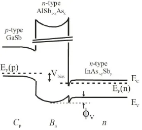
nBn photodetectors20 also convert incident light into an electrical current, but use a thin, wide bandgap barrier layer in place of the intrinsic region. The barrier layer, typically AlAsSb, is designed using bandgap engineering, yielding a large conduction band offset with respect to the absorption layer – typically InAs – but a small or negligible valence band offset. As a result,
2. Background Theory - 25
25
Figure 2.6: Intensity of propagating 1.55 μm radiation in an InAs diode, with 1 μm intrinsic region, according to Equation 2.26 (using an absorption coefficient from Ioffe4).
minority carriers flow freely, as illustrated in Figure 2.7. Generally, nBn detectors are tested under top-side illumination, i.e. radiation enters the detector from the right-hand-side of Figure
2.7, however reverse side illumination is also possible, and is preferred for focal plane arrays. Under a small applied operating bias, the electric field profile is concentrated across the barrier layer, rather than spreading into the narrow-bandgap absorption layer which is susceptible to
field. As a result, SRH generation and band-to-band tunnelling processes are virtually eliminated by the nBn design. n-type doping in the absorption and contact layers further pins
the Fermi level at the conduction band edge, away from mid-gap traps associated with SRH recombination. Finally, mesas are defined without etching through the barrier layer, creating a high shunt resistance for surface currents, which are also therefore almost eliminated by the
nBn design. Figure 2.8 shows the same data that was presented in Figure 2.2, but for the case of an nBn photodetector. In this case, the diffusion current depends only on the contribution
[image:35.595.73.411.72.327.2]2. Background Theory - 26
[image:36.595.79.413.343.608.2]26
Figure 2.7: nBn band diagram showing the generation of an electron-hole pair and the free
transport of holes (but not electrons) across the barrier layer.20
2. Background Theory - 27
27
increased compared with the previous figure, at 240 K. The absorber was modelled with an
n-type doping level of 1 × 1016 cm−3.
SAM-APD structures take advantage of the absorption properties of one material, i.e. a
narr-ow bandgap, and the multiplication properties of a second material, i.e. lnarr-ow excess noise behaviour, low dark currents, and/or high multiplication.21 The two are separated by a charge sheet (heavily doped, thin layer) which allows for the confinement of the peak field to the
multiplication layer, with only low field present in the absorber, as illustrated in Figure 2.9. Electron-hole pairs are generated in the absorption layer by excitation of electrons from the valence band into the conduction band, in the same way as for a p-i-n diode. Electrons (or holes
for the case of an n-type absorber) are then transported by the electric field into the multiplication region, where gain occurs.
Figure 2.9: Electric field profile for a simple SAM-APD structure under operating bias, as
2. Background Theory - 28
28 ix) Critical thickness modelling
Strain results from the growth of semiconductor epitaxial layers onto other layers with a diff-erent lattice constant. For small strains and thin layers, 2D planar growth proceeds, with the
strain being accommodated through a tetragonal distortion of the overlayer. However, as the overlayer mismatch and or thickness increase, a critical thickness occurs, beyond which it is no longer possible to accommodate the strain in this way. The strain is then accommodated
through faults in the crystal lattice known as dislocations. There are several models commo-nly used to calculate the critical thickness.22,23 According to Matthews and Blakeslee, the
critical thickness, hc, is given by22
hc =
b (1 −ν4)
4π(1 + ν)(ln ( hc
b) + 1) (2.27)
where ν is Poisson’s ratio for the epilayer, b is the Burger’s vector and is the natural misfit,
which is given according to
= |a − a0|
1
2(a + a0)
(2.28)
where a is the relaxed lattice constant of the epilayer, and a0 is the lattice constant of the
sub-strate. The model of Matthews and Blakeslee was derived using a force balance approach, considering the epitaxial strain to be the “driving force” counteracted by the tension due to
misfit dislocations. More recently, People and Bean derived a second model based on comp-aring the energies of the strained layer and the misfit dislocations, respectively. In principle,
the two approaches should give identical results (since both force balance and energy minimi-sation are fundamental concepts of Physics).24 However, it is suggested in [24] that People and Bean effectively considered a fixed dislocation density and a critical thickness at which all the
2. Background Theory - 29
29
the thickness at which the strain is first relieved through threading dislocations. According to
People and Bean, the critical thickness is given by23
hc =
b2(1 − 𝜈)
16π√22a(1 + ν)ln (
hc
b) (2.29)
where a is the epilayer lattice constant. The model of Matthews and Blakeslee provides a
conservative estimate, i.e. a layer grown at the critical thickness predicted by this model will never relax. It is suggested here that the epilayer thickness at which a significant portion of the
strain is relieved through misfit dislocations generally lies somewhere between values obtained from the two models. Equation 2.27 and Equation 2.29 are generally solved by tabulating the
2. Background Theory - 30
30
References
[1] A. Rogalski and Z. Orman, Infrared Phys 25, 3 (1985).
[2] S. M. Sze, Physics of Semiconductor Devices, 2ED (1981).
[3] P. Chakrabarti, A. Krier, and A. F. Morgan, IEEE Trans. Electron. Devices, Vol 50, No
10 (2003).
[4] NSM Archive - Physical Properties of Semiconductors, Ioffe Institute, http://www.ioffe.ru/SVA/NSM/Semicond/index.html
[5] H. S. Kim, E. Plis, A. Khoshakhlagh, S. Myers, N. Gautam, Y. D. Sharma, L. R. Dawson, S. Krishna, S. J. Lee, and S. K. Noh, Appl. Phys. Lett. 96, 033502 (2010).
[6] B. Van Zeghbroeck, Principles of Semiconductor Devices, Chapter 4: “p-n junctions” (2011).
[7] Agilent Impedance Measurement Handbook, 4ED. http://cp.literature.agilent.com/litweb/
pdf/5950-3000.pdf
[8] G. E. Stillman and C. M. Wolfe, “Avalanche Photodiodes,” in Infrared Detectors II, R. K.
Willardson and A. C. Beer, Eds., vol. 12 of Semiconductors and Semimetals, pp. 291-393. Academic Press, New York 1977.
[9] A. R. J. Marshall, C. H. Tan, M. J. Steer, and J. P. R. David, Appl. Phys. Lett. 93, 111107
(2008).
[10] R. K. Willardson, Semiconductors and Semimetals; Infrared Detectors, Academic Press
Inc. (1970).
[11] I. M. Baker, Selex UK (personal communication).
[12] R. J. McIntyre IEEE Trans. Electron Devices 13, 1, 164 (1966).
[13] D. S. Ong, K. F. Li, G. J. Rees, J. P. R. David, and P. N. Robson, J. Appl. Phys. 83, 6, 3426 (1998).
2. Background Theory - 31
31 Devices, 47, 3 (2000).
[15] S. L. Chan, Choo K. Y, in IEEE 2nd International Conference on Photonics, p1-5 (2011). [16] M. P. C. M. Krijn, Semicond. Sci. Technol. 6, 27 (1991).
[17] C. G. Van de Walle, Phys. Rev. B, 39, 3 (1989).
[18] I. Vurgaftman and J. R. Meyer, J. Appl. Phys, 89, 11 (2001).
[19] Matthew D. McCluskey, Eugene E. Haller, "Dopants and Defects in Semiconductors",
CRC Press (2012).
[20] S. Maimon and G. W. Wicks, Appl. Phys. Lett. 89, 151109 (2006).
[21] A. Krier (ed.), Mid-infrared Semiconductor Optoelectronics, Springer Series in Optical
Sciences, 118 (2006) p547-592 “High-speed Avalanche Photodiodes for the 2–5 µm Spectral Range”, M. P. Mikhailova and I. A. Andreev.
[22] J. W. Matthews and A. E. Blakeslee, J. Cryst. Growth, 27, 118 (1974). [23] R. People and J. C. Bean, Appl. Phys. Lett. 47, 322, (1985).
3. Literature Review - 32
32
(3) Literature review
This section first provides a summary of key literature relating to the lattice mismatched growth of both GaSb on GaAs and GaSb on Si. Previous reports of derivative devices (grown on GaAs substrates) are then examined. nBn detectors are treated next, via an exploration of papers by Maimon and Wicks at Rochester, NY, U.S.A, and Klipstein et. al. at SemiConductor Devices (SCD) in Israel. Further attention is given to nBn detectors based on strained-layer-superlattice (SLS) absorption regions, including to two-colour and complementary barrier designs. Finally, avalanche photodiodes (APDs) are explored, including those based on bina-ry InAs material, as well as more complicated separate absorption and multiplication (SAM) structures. These discussions are intended to provide a synopsis of previous works which made possible the research presented in sections 5-7, as well as providing a general overview of the literature.
i) Lattice mismatched growth and interfacial misfit arrays
Molecular beam epitaxial (MBE) growth of GaSb layers on GaAs substrates was reported in 1992 by Ivanov et. al.1 GaAs buffer layers of 200 nm thickness were deposited at 620 °C before
the growth of a GaSb buffer layer with a thickness of ~0.5 μm. Superlattice (SL) lay-ers (acting as threading dislocation filters) consisting of 10 repeats of 5 nm Al0.3Ga0.7Sb/5 nm GaSb or 5
nm AlSb/5nm GaSb were then grown at temperatures between 500 °C and 540 °C. This was followed in each case by a 1 μm-thick GaSb epilayer, grown at a rate of 0.6 MLs-1. Mirror-like epi-surfaces were reported for each sample after growth was complete. For the sample with an
AlSb/GaSb SL, the threading dislocation density (TDD) was found using tra-nsmission
electron microscopy (TEM). It was stated to be around 1010 cm−2 at the GaSb/ GaAs interface,
but this figure was reduced to 2 − 3 × 108 cm−2 within 200 – 400 nm GaSb film thickness. It
3. Literature Review - 33
33
first 0.5 μm of the GaSb overlayer was grown at 530 °C, but the remain-ing film thickness was
grown at 500 °C. This was evidenced via a reduction in full width at half maximum in x-ray diffraction (XRD) Bragg scans (154 arcsec for the two-temperature growth, compared with 160 – 215 arcsec for a single growth temperature of 530 °C). It was observed that the majority
of the population of misfit dislocations at the lattice-mismatched interface were of the pure-edge type, as arranged in a periodic network with a spacing of
~55 Å, illustrated in Figure 3.1. In addition, photoluminescence (PL) measurements for the mismatched samples were compared with similar measurements for the case of a similar film grown on native GaSb. However, it was found that the PL intensity recorded was lower by
three orders of magnitude for the growth on GaAs.
In 1997, Qian et. al. reported a reduction in the defect density for GaSb films grown on GaAs
[image:43.595.71.414.485.695.2]through the use of SL layers.2 These consisted of AlSb/GaSb and In0.11Ga0.89Sb/GaAs, resp-ectively. GaSb layers were grown at 550 °C and 0.8 MLs-1. An investigation of the relations-hip between the film thickness and the TDD was then carried out, both with no dislocation
3. Literature Review - 34
34
filter and with AlSb/GaSb and InGaSb/GaAs SL layers, respectively. Once again, TEM
im-ages showed arrays of misfit dislocations of the 90° type at the mismatched interface with a periodicity of ~55 Å. However, it was also reported that, by inspection of a larger volume of epilayer, there were still many threading dislocations. These were attributed to a minority
po-pulation of 60° misfits. Through measurements carried out for GaSb film thicknesses betw-een
0.5 – 14 μm, an empirical relationship between the TDD, ρ, and the film thickness, t, was
obtained
𝜌 = 109
𝑡5/3 (3.1)
where ρ has units of cm-2 and t has units of cm. The fitting used to determine the above
relati-onship is shown in Figure 3.2. Finally, a fully optimised growth using a 5-period GaSb/AlSb
SL was demonstrated, with a TDD of 5 × 107 cm−3 for a total film thickness of 2.2 μm.
Figure 3.2: Threading dislocation density, as a function of film thickness, for GaSb films
3. Literature Review - 35
35
In 2006, Huang and co-workers reported a realisation of low defect density GaSb layers
gro-wn on GaAs substrates.3 Strain relief was stated to occur exclusively via 90° (laterally propa-gating) dislocations, i.e. without the presence of 60° misfit dislocations. The occurrence of 60° misfit dislocations was thought to be associated with the coalescence of islands of GaSb in the
early stages of growth, and the choice of growth temperature, with growth at 510 °C resulting in an elimination of 60° misfits. The authors describe the growth of a GaAs buffer layer at 560
°C. A special desorption step was then described, where As adatoms were remo-ved from the growth surface by closing the As valve, leaving the growth surface Ga termi-nated. Sb2 flux was then applied followed by a reduction in temperature to 510 °C. GaSb gro-wth then
proceeded with a reflection high energy electron diffraction (RHEED) pattern of 1 × 3
reconstruction exhibited. The misfit array is illustrated using cross-sectional transm-ission
electron microscopy (TEM) in Figure 3.3. The dark spots were stated to correspond to misfit sites and an absence of visible threading dislocations cited. The misfit separation was measured (from Figure 3.3) to be 5.6 nm, corresponding to 13 lattice sites of GaSb and 14 lattice sites of
GaAs. One in every 14 Ga atoms thus forms a dangling bond. For samples gro-wn under optimised growth conditions, KOH etch pit defect density (EPDD) defect density figures 7 ×
105 cm−2 were reported (for an epilayer thickness of 3.1 μm). It was further sta-ted that
growths carried out at 480 °C and 540 °C had larger EPDD figures, but these were not quoted. No control sample (no comparison drawn with non-IMF growth) was reported.
In 2009, the same authors reported plan-view TEM studies of GaSb epilayers grown on GaAs susbtrates via the IMF array growth mode.4 The work introduces the term interfacial misfit (IMF) array and refers to this as a new growth mode. However, the network of 90° misfit dislocations reported is also itself referred to as “an IMF”. A 2 × 8 RHEED pattern was noted
to be observed following the application of Sb2 flux, believed to be associated with the
3. Literature Review - 36
36
Figure 3.3: Cross-sectional TEM image showing a highly periodic array of 90° misfit dislo-cations (an IMF array) at the interface between a GaSb epilayer and a GaAs buffer layer.3
figure was explained to be based on counting visible dislocations in plan-view TEM images of a sample with a 5 μm-thick GaSb epilayer. An example of such an image is reproduced in
Figure 3.4.
In 2011, workers at the University of Maryland reported details of the structural properties of
lattice mismatched films grown on GaAs substrates using IMF arrays.5 These films consisted of binary GaSb, InAs and InP, as well as ternary and quaternary alloys. It was reported that the
films achieved full relaxation within a few monolayers of the interface. X-ray diffraction (XRD) reciprocal space mapping was used to determine the degree of relaxation. For the GaSb film in particular, the article points out overgrowth was carried out without first soa-king the