Doping of Self-Catalyzed Nanowires under the Influence of
Droplets
Yunyan Zhang,†* Zhiyuan Sun,‡⊥ Ana M. Sanchez,#⊥
Manfred Ramsteiner,§⊥
Martin Aagesen,‖ Jiang Wu,† Dongyoung Kim,† Pamela Jurczak,† Suguo Huo,¶ Lincoln J. Lauhon,‡ and Huiyun Liu†
† Department of Electronic and Electrical Engineering, University College London, London WC1E 7JE,
United Kingdom;
‡ Department of Materials Science and Engineering, Northwestern University, 2220 Campus Drive,
Evanston, Illinois 60208-3108, United States
# Department of Physics, University of Warwick, Coventry CV4 7AL, United Kingdom § Paul-Drude-Institut für Festkörperelektronik, Hausvogteiplatz 5–7, 10117 Berlin, Germany
‖ Center for Quantum Devices, Niels Bohr Institute, University of Copenhagen, Universitetsparken 5,
2100 Copenhagen, Denmark
¶ London Centre for Nanotechnology, University College London, London WC1H 0AH, United Kingdom
Abstract: Controlled and reproducible doping is essential for nanowires (NWs) to
realize their functions. However, for the widely-used self-catalyzed vapor-liquid-solid
(VLS) growth mode, the doping mechanism is far from clear, as the participation of the
nanoscale liquid phase makes the doping environment highly complex and significantly
different from that of the thin film growth. Here, the doping mechanism of
self-catalyzed NWs and the influence of self-catalytic droplets on the doping process are
the first time to be incorporated into NWs predominantly through the Ga droplet that is
observed to be beneficial for setting up thermodynamic equilibrium at the growth front.
Be dopants are, thus substitutional on Ga sites and redundant Be atoms are accumulated
inside the Ga droplets when NWs are saturated, leading to the change of the Ga droplet
properties and causing the growth of phase-pure zincblende NWs. This study is an
essential step toward the design and fabrication of nanowire devices.
Key words:nanowire, Ga droplet, Be doping, incorporation path, phase pure
Nanowires (NWs) have attracted significant attention, due to their novel
mechanical, optical and electronic properties that are not present in the thin film
counterparts1−5 and diverse types of NW-based devices have been demonstrated across
a wide range of areas, such as electronics, photonics, biochemistry and
medicine 6 − 13 Continuing improvements in individual device performance, in combination with the ability to monolithically integrate NWs onto low-cost substrates,
e.g. silicon (Si), makes them very promising for future technologies. In order to realize
foundational device structures like p-i-n diodes and tunnel junctions, controlled and
reproducible impurity doping is essential. Moreover, NW devices have higher
requirements on doping than their bulk counter parts, such as the density and the spatial
distribution of dopants.14 Understanding NW doping mechanisms is therefore a necessary prerequisite to control the NW conductivity for device fabrication.
One of the most widely used approaches to fabricate III-V NWs is
nano-sized liquid droplet to transport growth material to the liquid solid growth
interface. All the materials incorporated into the core NWs need to go through them.
The liquid droplet strongly influences crystal structure,16 morphology,17 and dopant incorporation18 through its chemical and mechanical interactions at the vapor-liquid-solid and liquid-vapor-liquid-solid interfaces. Due to the participation of the liquid phase, the NW
growth mechanism is much more complex than those of traditional thin film structures
that use the vapor-solid growth mode. Although the droplet in VLS growth effectively
promotes growth along a particular direction, parasitic vapor solid (VS) growth may
also occur on the exposed sidewalls of the nanowire. VLS and VS dopant incorporation pathways may produce distinct active dopant concentrations; because both pathways are influenced by growth conditions, nanowires can exhibit complex and distinct active dopant profiles.19 The complexity in growth mode brings significant challenges in
understanding some fundamental principles of doping, e.g. the dominant doping path
of III-V NWs.20,21
Although there have been intensive studies focusing on the mechanisms,
limitations and influences of dopant incorporation on VLS-grown NW in the past few
years,22,25−32 most of the reported work was conducted using foreign-metal-catalyzed
growth (e.g. Au). More recently, the self-catalyzed growth mode has received
increasing attention because it can avoid the possible contamination by foreign metals
and has the advantage to consume the droplet for a subsequent VS shell growth.33 However, its growth condition is typically different from that of the Au-catalyzed
melting point of the material being grown, which is often far above the growth
temperature of Au-catalyzed mode.36,37 This temperature difference could influence the droplet performance and the material deposition. Thus, not all findings from
foreign-metal-catalyzed growth can be transferred directly to self-catalyzed nanowires.
The mechanism of doping self-catalyzed NWs is still far from clear and there still lack
of consistent conclusions regarding some fundamental questions, such as the influence
of the droplet in the doping process.
In this paper, the doping of self-catalyed NWs is investigated systematically using
GaAs NWs and Be dopants. Be dopants are found, for the first time, to incorporate
predominantly through the Ga droplet in our growth condition, which is different from
previous reports that Be atoms incorporate preferentially via the NW side facets.27 The
thermodynamic equilibrium maintained by the Ga droplet leads to substitutional doping
of Be at Ga sites while excess Be accumulates in the Ga droplet. We also show that the
formation of a Ga-Be alloy droplet alloy leads to the growth of pure zinc blende (ZB)
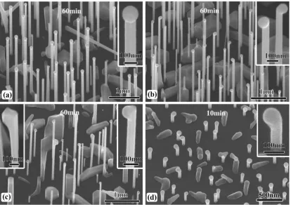
Figure 1. SEM image of GaAs NWs with nominal Be doping concentration of (a)
0, (b) 1.6×10¹⁸, and (c), (d) 1.28×10¹⁹/cm3. (a)~(c) have a growth duration of 1hour, while (d) has a growth duration of only 10 minutes.
Figure 1 examines the changes in Ga droplet and GaAs nanowire morphology
induced by a Be flux in a self-catalyzed growth process. During the cooling process
after NW growth, both Ga and As fluxes are switched off to keep the Ga droplets.
Nanowires grown without Be are uniform in diameter along the nanowire length
(Figure 1a), indicating negligible parasitic sidewall growth, and the round Ga droplet
centered at the top of each nanowire indicates a VLS growth mode. If a Be flux is
introduced at a nominal concentration of 1.6×10¹⁸/cm3, the nanowires remain uniform in diameter for a 60-minute growth, but the droplets are displaced from the nanowire
interface energies leading to droplet sidewall wetting. If instead growth is allowed to
continue from this point for another 20 minutes, but in the absence of Be flux, a centered
droplet is observed and no kinking results (Figure S1), confirming that Be induces the
droplet instability. Furthermore, if the Be flux is increased to a nominal doping
concentration to 1.28×10¹⁹/cm3 (Figure 1c), the droplet slides completely to the side wall (right inset) and some of the droplets solidify (left inset) which is similar to
changes in droplet morphology shown previously.29,38-42 We observe that the nanowires with intact droplets at the tip (right inset of Figure 1c, Figure 6l and Figure 6m) are
uniform in diameter along their lengths, which suggests that the droplet size does not
change substantially during growth. Hence, we rule out the possibility that sidewall
wetting occurs due a simple increase in droplet size. Instead, the droplet instability is
attributed to a surface energy imbalance caused by the increase in Be concentration
inside the droplets (without a significant change in volume); this modifies the surface
energies to the point that the maximum stable contact angle is exceeded.43
To test this hypothesis, nanowires were grown for a shorter duration of 10 mins
at the same Be flux. As can be seen in Figure 1d, the nanowires are uniform in diameter
along their lengths. Furthermore, the nanowires are terminated with a droplet at the top,
and none of the droplets are on the sidewalls, consistent with lower Be concentration
inside the droplets compared to the sample shown in Figure 1c. Indeed, the nanowires
in Figure 1d are a case intermediate to that of Figure 1b and c. Hence, we propose that
the Be concentration increases gradually during growth. At some critical concentration,
VLS growth termination.
Figure 2. Illustration of growth mechanism in the self-catalyzed NW growth with
Be doping. (a) Initial VLS NW growth. (b) Sidewall wetting of the droplet due to the
Be accumulation and hence change of surface energy. (c) Solidification of Ga droplet.
The VLS-growth failure induced by Be doping can thus be explained by the Be
accumulation model shown in Figure 2. At an early stage shown in Figure 2a, the NW
is growing normally similarly to undoped NWs with a droplet on top. Because the NW
sidewalls consist of {110} facets that with low surface energy, parasitic VS growth at
this high growth temperature is limited, and thus the NWs have a uniform diameter.
[44,45] Not all the Be can be incorporated into the NW crystal and instead accumulates
inside the Ga droplet. Thus, the Be concentration increases gradually during VLS
growth until the change in Ga droplet surface energy causes sidewall wetting and the
loss of the droplet from the top of the NW (Figure 2b). The droplet subsequently
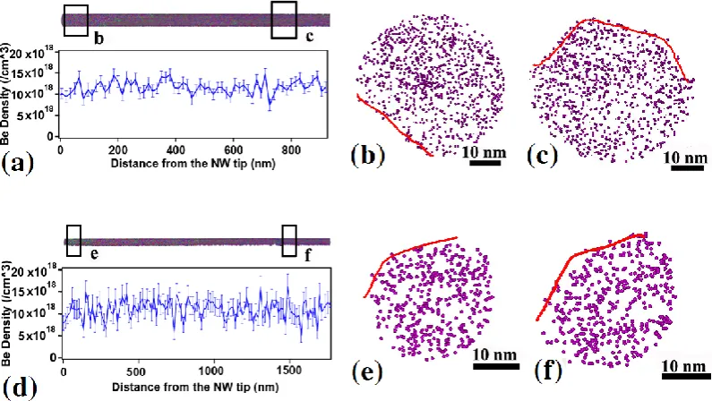
Figure 3. APT analysis of NWs with doping density of (a)~(c) 1.28×10¹⁹/cm3 and (d)~(f) 6.4×10¹⁸/cm3. (a) and (d) Be concentration profile along each NW length. Insets above are three-dimensional tomographic reconstructions of each NW. (b) (c) and (e)
(f) Radial Be atom distribution maps of the 100 nm segments marked in the square of
(a) and (d), respectively. Due to small measurement window, only part of NW surface
(marked with red lines) can be reconstructed.
The invariant diameter of the nanowires indicates that VLS growth dominates
sidewall (vapor-solid) growth, so a VLS dopant incorporation mechanism might also
be expected. However, the accumulation of Be in the droplet implies that the dopant
incorporation rate across the liquid-solid interface may not be simply proportional to
the Be flux. Furthermore, prior studies have made conflicting claims regarding the
dopant incorporation mechanisms, albeit using growth conditions that vary in the
mechanism for Ga-assisted VLS growth of GaAs nanowires, atom-probe tomography
(APT) measurements46−48 were performed to 60-min-grown NWs with nominal doping concentrations of 1.28×10¹⁹/cm3 (Sample A) and 6.4×10¹⁸/cm3 (Sample B). The NWs used in the measurement are all uniform in diameter along the length, showing minute
parasitic sidewall growth. Sample B has a length of ~3.6 μm. In contrast, Sample A has
a length of ~2 μm and its droplet is on the sidewall (Figure 5l and m), indicating that
the axial growth stopped earlier than that of Sample B and/or the dissolved Be reduced
the As flux at the liquid-solid interface.49 The APT measurement started from the nanowire tip and encompasses more than half of the total length. We find that nanowires
A and B are uniformly doped to ~1.1×10¹⁹/cm3 both along the length of the nanowires (Figure 3a,d), and radially across the diameter (Figure 3,b,c,e,f). This core doping
concentration is comparable to that found by Boulanger et al,50 who used secondary
ion mass spectroscopy to measure an averaged value of ~5×10¹⁸/cm3, which corresponded to the nominal doping level based on the Be flux.
The APT analysis also allows us to directly address the dopant incorporation
mechanism; tilting the nanowire with respect to the APT analysis direction, the oxidized
side facets (red lines in Figure 3b,c,e,f) can be brought into the field of view (see also
Figure S2).51 There is no evidence of Be accumulation at the nanowire surface or Be
segregation inside the nanowire crystal, suggesting that dopant incorporation occurs
predominantly through the Ga droplet. This is in contrast the conclusion of Casadei et
same growth temperature, but with slightly higher V/III ratio and dopant flux. If most
of the Be were diffusing in from the sidewalls of our nanowires, one would expect the
tip regions (Figure 3b,e) to be less doped than the middle regions (Figure 3c,f), which
is not the case.
We note that sample A was grown at twice the Be flux as sample B, yet both
samples have the same dopant concentration over the measured lengths, which indicates
that the steady-state rate of Be incorporation is limited by the solubility of Be in GaAs
for the growth conditions used (and further supports doping from the liquid-solid
interface). This is confirmed by the observation that the Be concentration in the Ga
droplet increases with increasing growth time. Furthermore, Be is rejected from the
growth interface of sample A at a higher rate than for sample B, which is confirmed by
the observations that the droplet is destabilized earlier in growth for sample A (Figure
1c,d) compared to sample B (Figure 1b). If one assumes that the growth interface is
near equilibrium, one expects the Be atoms to occupy primarily the configuration of
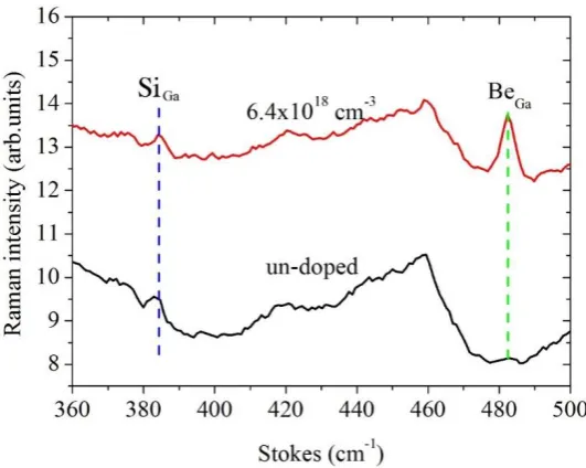
Figure 4. Raman spectra of NWs without and with doping concentration of
6.4×10¹⁸/cm3.
The configuration of Be atoms inside the Be-saturated NW crystals was studied by
Raman spectroscopy of local vibrational modes (LVM). 29 The Raman spectrum, shown in Figure 4, exhibits the LVM of substitutional Be on Ga site (BeGa) at 482 cm-1
superimposed on a background of second-order phonon scattering.53 Consistent with
our assignment, the relative LVM line intensity in the Raman spectrum of the Be doped
nanowires corresponds to a BeGa concentration on the order of 0.5 to 1.0 x 10¹⁹/cm3,53
which is comparable to the total concentration of incorporated Be measured by APT as
shown in Figure 2.
The weaker Raman peak at 384 cm-1 has been attributed both to the LVM of Si on
Ga site (SiGa)54 or to Be related defects29 that were tentatively assigned to complexes
including a Be atom on interstitial site (Bei) in GaAs NWs with extremely heavy Be
[image:12.595.170.436.92.304.2]of nominally undoped nanowires grown under the same conditions as the doped
samples is also shown in Figure 4 (black line). Since the line at 384 cm-1 is detected with comparable Raman intensity in both Be doped and nominally undoped NWs, we
attribute it to SiGa incorporated into the GaAs nanowire via the substrate, a small portion
of which is dissolved by the Ga droplets.55 Therefore, these doped NWs contain predominantly Be atoms on Ga sites, which is consistent with the claim that the near
equilibrium liquid-solid growth interface inhibits the formation of high configuration
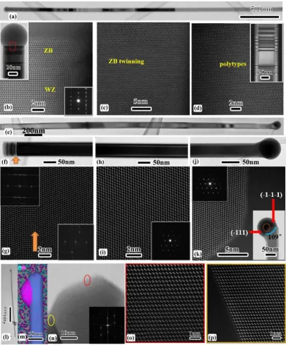
Figure 5. (a)~(d) GaAs NWs without doping. (a) Low magnification TEM image
of the whole NW and atomic resolution ADF-STEM image of (b) tip, (c) middle of
body, and (d) bottom of the NW shown in (a). The insets in (b) are the low magnification
TEM image and the selected area electron diffraction pattern of the tip portion. The
insets in (d) correspond to the low magnification TEM image of the bottom portion of
Low magnification TEM image shows the entire NW. Low magnification and atomic
resolution ADF-STEM images of (f) (g) bottom, (h) (i) middle of body, and (j) (k) top
of the NW. The orange arrows shown in (f) and (g) indicate similar positions. The upper
left and lower right insets show the electron diffraction patterns of the defect and
defect-free regions at left and right-hand side of the orange arrow, respectively. The insets in
(i) corresponds to the electron diffraction pattern of (h). The insets in (k) are the low
magnification TEM image and the electron diffraction pattern of the top part of the NW.
(l)~(p) GaAs NWs with a nominal doping concentration of 1.28×10¹⁹/cm3. (l) Low magnification TEM image. (m) EDX mapping of the top part of the NW shown in (l).
(n) Atomic resolution ADF-STEM image of the top. The inset in (n) is the electron
diffraction pattern of the top part. (o) and (p) atomic resolution ADF STEM image of
the are marked in (n) with a red and yellow circle respectively.
The accumulation of Be in the catalyst droplet has a beneficial effect on crystal
structure. A typical nanowire grown without intentional doping exhibits stacking faults
and polytypism as shown in TEM and Annular Dark Field (ADF)-STEM images in
Figure 5a-d. The tip of the nanowire is dominated by single twins and segments of WZ
and ZB (Figure 5b), the body of the nanowire contains many single twins (Figure 5c),
and the bottom of the nanowire is a mixture of ZB and WZ polytypes (Figure 5d). In
contrast, the nanowire grown with a Be flux has a greatly reduced defect density (Figure
the very bottom (Figure 5f,g). From the high-resolution images shown in Figures 4i and
k, it is clear that above the bottom segment, the nanowire has a defect-free ZB structure
up to the top-most bilayer. The suppression of WZ nucleation during growth is likely
due to the lowering of droplet supersaturation and/or surface energy due Be
accumulation to form a Be-Ga alloy droplet.56−58 It has been reported that doping can lower the droplet surface energy and increase the contact angle of the particle-NW
interface, leading to an increase of the barrier for WZ nucleation.56 Consistent with this assumption, the defective region at the bottom was formed at the earliest stage of the
growth, when the Be concentration inside the droplet is very low. With the increase in
growth time and accumulation of Be inside the droplet, ZB nucleation becomes favored.
Eventually, Be accumulation also leads to wetting of the sidewall and the development
of multiple (111) growth facets. Figure 5k shows that a new (-111) facet has formed
with an angle of 109° relative to the (-1-1-1) facet. This is in contrast to the undoped
nanowires that exhibit a single dominant (111) facet at the droplet/nanowire interface
(inset of Figure 5b). For nanowires grown with a higher nominal doping density of
1.28×10¹⁹/cm3, the droplet may move entirely to the sidewall, as seen in Figures 5l and m. The nanowire has a pure ZB crystal structure up to top most bilayer (Figure 5n-p),
as observed for the nanowire in Figure 4e, and the droplet/nanowire interface also has
a pure ZB crystal structure all the way to the growth front (Figure 5n,p).
In summary, Be atoms are found to incorporate into nanowires predominantly
through the Ga catalyst droplets during the Ga-assisted VLS growth of GaAs nanowires
significant amounts of Be are retained in the droplet. Raman analysis of local
vibrational modes suggest that most Be incorporates substitutionally for Ga. This is in
stark contrast to thin film vapor-solid growth at high dopant fluxes, which can result in
segregation and precipitation, leading to a deterioration in material quality. [59−63] The formation of a Be-Ga alloy droplet also has the beneficial effect of suppressing WZ
nucleation and enabling the growth of a pure ZB crystal up to the top-most bilayer.
These results not only guide the control and development of NW doping methods, but
also provide valuable information for understanding the basic physics of doping
nanoscale materials through a liquid phase.
Experimental Section
NW growth: The self-catalyzed GaAs NWs were grown directly on p-type Si(111)
substrates by means of solid-source III−V molecular beam epitaxy (MBE). [64,65] GaAs NWs were grown with a Ga beam equivalent pressure, V/III flux ratio, substrate
temperature, growth duration and nominal doping concentration (characterized in thin
film growth) of 8.41×10⁻⁸ Torr, 44, ~630°C, 1 hour and 0~1.28×10¹⁹/cm3, respectively. The substrate temperature was measured by pyrometer.
Focus ion beam/scanning electron microscope (FIB/SEM): The NW morphology
was measured with a Zeiss XB 1540 FIB/SEM system.
Transmission electron microscopy (TEM): Simple scraping of the NWs onto a
lacey carbon support was used to prepare TEM specimens. The TEM measurements
operating at 200 kV.
Atom-probe tomography measurements (APT): APT samples were prepared in a
Helios dual beam focused ion beam system with Kleindieck nanomanipulator.66 The NWs vertically grown on substrate were firstly welded to a sharp tungsten needle and
then transferred to a silicon micropost. APT was performed on a local-electrode
atom-probe tomography 4000 X Si at a base temperature of 30 K and base pressure of 2 x 10 -11 Torr. The evaporation of the atoms was controlled by 355 nm picosecond focused
laser beam at a pulse frequency of 500 kHz and at an evaporation rate of 1~2 atoms per
100 laser pulse. The NWs were tilted respect to the APT analysis direction intentionally
during the sample preparation to enhance the APT field of view and get the surface
doping information of the NW. APT data were reconstructed in the commercial
software IVAS 3.6.12 (Cameca, Madison, WI). The reconstruction parameters were
adjusted to reproduce the GaAs (111) interplanar distance near the 111 evaporation pole.
Raman spectroscopy: The Raman spectroscopic measurementswere performed at
low temperature (10 K) in backscattering geometry from the side facets of NWs
dispersed on a gold-coated Si substrate. For optical excitation, the 405-nm line of a
solid-state laser was focused by a microscope objective onto the NWs. The
backscattered light was collected by the same objective, spectrally dispersed by an
80-cm spectrograph (LabRam HR Evolution, Horiba/Jobin Yvon) and detected with a
liquid-nitrogen-cooled charge-coupled device. The concentration of Be on Ga sites has
been estimated by the procedure described in Ref. 53. In this article, it is shown that the
quantitative calibration, the LVM signal has been normalized to the strength of an
intrinsic second-order phonon feature in the Raman spectrum. This procedure
eliminates experimental difficulties in measuring absolute scattering intensities. In the
case of NWs, the not exactly defined Raman scattering geometry is possibly a
non-negligible source of uncertainty in the deduced Be concentrations. Consequently, we
mention in our manuscript only a relatively large concentration range. Nevertheless, the
comparison of the Be concentrations between different NW samples is much more
precise, due to the same deviation from the exactly defined scattering geometry.
ASSOCIATED CONTENT
Supporting Information
GaAs NWs produced by 60 mins Be-doped growth and 20 mins undoped growth.
Oxygen distribution map in the NW cross-section
Author Information
Corresponding Author: Y. Zhang
*E-mail: [email protected]
Author Contributions:
⊥ Z. Sun, A. M. Sanchez, M. Ramsteiner contributed equally to this work.
Notes:
Acknowledgements:
The authors acknowledge the support of Leverhulme Trust, National Science
Foundation (NSF, DMR-1611341) and Binational Science Foundation (BSF, 2012088)
References:
(1) Lieber, C. M.; Wang, Z. L. MRS Bull. 2007, 32, 99−108.
(2)Zhang, Y.; Wu, J.; Aagesen, M.; Liu, H. J. Phys. D: Appl. Phys. 2015, 48, 463001. (3) Yan, R.; Gargas, D.; Yang, P. Nat. Photonics2009, 3, 569−576.
(4) Dasgupta, N. P.; Sun, J.; Liu, C.; Brittman, S.; Andrews, S. C.; Lim, J.; Gao, H.; Yan, R.; Yang, P. Adv. Mater.2014, 26, 2137.
(5) Yang, P.; Yan, R.; Fardy, M. Nano Lett.2010, 10, 1529−1536.
(6)Zheng, G. F.; Patolsky, F.; Cui, Y.; Wang, W. U.; Lieber, C. M. Nat. Biotechnol. 2005, 23, 1294.
(7) Huang, Y.; Duan, X.; Cui, Y.; Lauhon, L. J.; Kim, K. H. & Lieber, C. M. Science 2001, 294, 1313.
(8) De Franceschi, S.; van Dam, J. A.; Bakkers, E. P. A. M.; Feiner, L. F.; Gurevich, L.; Kouwenhoven, L. P. Appl. Phys. Lett.2003, 83, 344.
(9) Doh, Y. J.; van Dam, J. A.; Roest, A. L.; Bakkers, E. P. A. M.; Kouwenhoven, L. P.; De Franceschi, S. Science2005, 309, 272.
(10) Gudiksen, M. S.; Lauhon, L. J.; Wang, J.; Smith, D. C.; Lieber, C. M. Nature2002, 415, 617.
(11) Holm, J. V.; Jørgensen, H. I.; Krogstrup, P.; Nygård, J.; Liu, H.; Aagesen, M. Nat. Commun.2013, 4, 1498.
P. Science2001, 292, 1897.
(13) Wu, J.; Ramsay, A.; Sanchez, A. M.; Zhang, Y.; Kim, D.; Brossard, F. S. F.; Salamo, G. G. Aagesen, M.; Wang, Z.; Liu, H. Nano Lett.2016, 16, 504.
(14) Wallentin, J.; Borgström, M. T. J. Mater. Res.2011, 26, 2142. (15) Wagner, R. S.; Ellis, W. C. Appl. Phys. Lett. 1964, 4, 89−90.
(16) Jacobsson, D.; Panciera, F.; Tersoff, J.; Reuter, M. C.; Lehmann, S.; Hofmann, S.; Dick, K. A.; Ross, F. M. Nature, 2016, 531, 317-322.
(17) Schwarz, K. W.; Tersoff, J.; Kodambaka, S.; & Ross, F. M. Physical review letters,2014. 113, 055501.
(18) Connell, J. G.; Yoon, K.; Perea, D. E.; Schwalbach, E. J.; Voorhees, P. W.; Lauhon, L. J.
Nano letters, 2012, 13, 199-206.
(19) Amit, I.; Givan, U.; Connell, J. G.; Paul, D. F.; Hammond, J. S.; Lauhon, L. J.; & Rosenwaks, Y. Nano letters, 2013, 13(6), 2598.
(20) Stichtenoth, D.; Wegener, K.; Gutsche, C.; Regolin, I.; Tegude, F. J.; Prost, W.; Seibt, M.; Ronning, C. Appl. Phys. Lett.2008, 92, 163107.
(21) Li, H. Y.; Wunnicke, O.; Borgström, M. T.; Immink, W. G. G.; Van Weert, M. H. M.; Verheijen, M. A.; Bakkers, E. P. A. M. Nano lett.2007, 7, 1144.
(22) Gutsche, C.; Regolin, I.; Blekker, K.; Lysov, A.; Prost, W.; Tegude, F. J. J. Appl. Phys.
2009, 105, 024305.
(23) Zhang, G.; Tateno, K.; Suzuki, S.; Gotoh, H.; Sogawa, T. J. Phys. Chem. C2011, 115, 2923.
174303.
(25) Borgström, M. T.; Norberg, E.; Wickert, P.; Nilsson, H. A.; Trägårdh, J.; Dick, K. A.; Statkute, G.; Ramvall, P.; Deppert, K.; Samuelson, L. Nanotechnology2008, 19, 445602. (26) Suomalainen, S.; Hakkarainen, T. V.; Salminen, T.; Koskinen, R.; Honkanen, M.; Luna,
E.; Guina, M. Appl. Phys. Lett.2015, 107, 012101.
(27) Casadei, A.; Krogstrup, P.; Heiss, M.; Röhr, J. A.; Colombo, C.; Ruelle, T.; Upadhyay, S.; Sørensen, C. B.; Nygård, J. & i Morral, A. F. Appl. Phys. Lett.2013, 102, 013117.
(28) Wolf, D.; Lichte, H.; Pozzi, G.; Prete, P.; & Lovergine, N. Applied Physics Letters, 2011, 98, 264103.
(29) Hilse, M.; Ramsteiner, M.; Breuer, S.; Geelhaar, L.; & Riechert, H. Applied Physics Letters,2010, 96, 193104.
(30) Chia, A. C. E.; Boulanger, J. P.; & LaPierre, R. R. Nanotechnology, 2013, 24, 045701. (31) Morkötter, S.; Jeon, N.; Rudolph, D.; Loitsch, B.; Spirkoska, D.; Hoffmann, E.;
Döblinger, M.; Matich, S.; Finley, J. J.; Lauhon, L. J.; Abstreiter, G.; Koblmüller, G. Nano letters, 2015,.15, 3295.
(32) Ketterer, B.; Mikheev, E.; Uccelli, E.; Fontcuberta i Morral, A. Appl. Phys. Lett.2010, 97, 223103.
(33) Dubrovskii, V. G.; Xu, T.; Álvarez, A. D.; Plissard, S. R.; Caroff, P.; Glas, F.; Grandidier, B. Nano letters, 2015, 15, 5580.
02L114.
(35) Dufouleur, J.; Colombo, C.; Garma, T.; Ketterer, B.; Uccelli, E.; Nicotra, M. & Fontcuberta i Morral, A. Nano lett.;2010, 10, 1734.
(36) Zhang, Y.; Aagesen, M.; Holm, J. V.; Jørgensen, H. I.; Wu, J.; Liu, H. Nano Lett. 2013, 13, 3897−3902.
(37) Joyce, H. J.; Gao, Q.; Tan, H. H.; Jagadish, C.; Kim, Y.; Zhang, X.; Guo, Y.; Zou, J. Nano lett.2007, 7, 921.
(38) Kelrich, A.; Sorias, O.; Calahorra, Y.; Kauffmann, Y.; Gladstone, R.; Cohen, S.; Ritter, D.
Nano letters, 2016, 16, 2837-2844.
(39) de la Mata, M.; Leturcq, R.; Plissard, S. R.; Rolland, C.; Magén, C.; Arbiol, J.; Caroff, P.
Nano letters, 2016, 16, 825-833.
(40)Hocevar, M.; Immink, G.; Verheijen, M.; Akopian, N.; Zwiller, V.; Kouwenhoven, L.;
Bakkers, E. arXiv preprint arXiv:1210.8350. 2012
(41) Yuan, X.; Caroff, P.; Wong‐Leung, J.; Fu, L.; Tan, H. H.; Jagadish, C. Advanced Materials, 2015, 27, 6096-6103.
(42) Wang, J.; Plissard, S. R.; Verheijen, M. A.; Feiner, L. F.; Cavalli, A.; Bakkers, E.
P. Nano letters, 2013, 13, 3802-3806.
(43) Nebol'Sin, V. A.; Shchetinin, A. A. Inorganic materials, 2003, 39, 899-903.
(44) Zhang, Y.; Sanchez, A. M.; Wu, J.; Aagesen, M.; Holm, J. V.; Beanland, R.; Ward, T.; Liu, H. Nano lett.2015, 15, 3128.
(45) Zheng, C.; Wong-Leung, J.; Gao, Q.; Tan, H. H.; Jagadish, C.; & Etheridge, J. Nano lett.;
(46) Jeon, N.; Loitsch, B.; Morkoetter, S.; Abstreiter, G.; Finley, J.; Krenner, H. J.; Koblmueller, G.; Lauhon, L. J. ACS nano2015, 9, 8335.
(47)Seidman, D. N.; Stiller, K. MRS bull.2009, 34, 717.
(48) Sun, Z.; Hazut, O.; Huang, B. C.; Chiu, Y. P.; Chang, C. S.; Yerushalmi, R.; Lauhon, L. J.; Seidman, D. N. Nano lett.2016, 16, 4490-4500.
(49) Nimmatoori, P., Zhang, Q., Dickey, E. C., & Redwing, J. M. Nanotechnology, 2008, 20,
025607.
(50) Boulanger, J. P.; Chia, A. C. E.; Wood, B.; Yazdi, S.; Kasama, T.; Aagesen, M.; LaPierre, R. R. IEEE Journal of Photovoltaics, 2016, 6, 661.
(51) Chen, W.; Pareige, P.; Castro, C.; Xu, T.; Grandidier, B.; Stiévenard, D.; Roca i Cabarrocas, P. J. Appl. Phys.2015, 118, 104301.
(52) Komsa, H. P.; Arola, E.; Pakarinen, J.; Peng, C. S.; Rantala, T. T. Phys. Rev. B2009, 79, 115208.
(53) Wagner, J.; Maier, M.; Murray, R.; Newman, R. C.; Beall, R. B.; Harris, J. J. J. Appl. Phys.1991, 69, 971.
(54) Murray, R.; Newman, R. C.; Sangster, M. J. L.; Beall, R. B.; Harris, J. J.; Wright, P. J.; Wagner, J.; Ramsteiner, M. J. Appl. Phys.1989, 66, 2589.
(55) Ihn, S. G.; Song, J. I.; Kim, Y. H.; Lee, J. Y.; Ahn, I. H. IEEE T. Nanotechnol.2007, 6, 384-389.
(56) Wallentin, J.; Ek, M.; Wallenberg, L. R.; Samuelson, L.; Deppert, K.; Borgstrogm, M. T.
Nano Lett.2010, 10, 4807.
Enckevort, W. J. P.; Vlieg, E.; Bakkers, E. P. A. M. Nature2008, 456, 369.
(58) Wallentin, J.; Mergenthaler, K.; Ek, M.; Wallenberg, L. R.; Samuelson, L.; Deppert, K.; Pistol, M. E. & Borgstrom, M. T. Nano lett.2011, 11, 2286.
(59) Bresse, J. F.; Papadopoulo, A. C. Appl. Phys. Lett.1987, 51, 183.
(60) Duhamel, N.; Henoc, P.; Alexandre, F.; Rao, E. V. K. Appl. Phys. Lett.1981, 39, 49. (61) Enquist, P.; Wicks, G. W.; Eastman, L. F.; Hitzman, C. J. Appl. Phys.1985, 58, 4130. (62) Ivanov, S. V.; Kop'ev, P. S.; Ledentsov, N. N. J. Cryst. growth1991, 108, 661.
(63) Morita, M.; Kobayashi, K.; Suzuki, T.; Okano, Y. Japanese J. Appl. Phys.1989, 28, 553. (64) Zhang, Y.; Sanchez, A. M.; Sun, Y.; Wu, J.; Aagesen, M.; Huo, S.; Liu, H. Nano lett.;
2016, 16, 1237.
(65) Zhang, Y.; Wu, J.; Aagesen, M.; Holm, J.; Hatch, S.; Tang, M.; Huo, S.; Liu, H. Nano lett.2014, 14, 4542.
(66) Sun, Z.; Tzaguy, A.; Hazut, O.; Lauhon, L. J.; Yerushalmi, R.; Seidman, D. N. Nano Lett.