warwick.ac.uk/lib-publications
A Thesis Submitted for the Degree of PhD at the University of Warwick
Permanent WRAP URL:
http://wrap.warwick.ac.uk/91299
Copyright and reuse:
This thesis is made available online and is protected by original copyright.
Please scroll down to view the document itself.
Please refer to the repository record for this item for information to help you to cite it.
Our policy information is available from the repository home page.
Germanium As a Platform For Semiconductor
Spintronics
by
Jamie Matthew Foronda
Thesis
Submitted to the University of Warwick
for the degree of
Doctor of Philosophy
Department of Physics
Contents
List of Tables v
List of Figures vi
Acknowledgments xvii
Declarations xviii
0.1 Publications . . . xix
0.1.1 Publications Cited in This Thesis . . . xix
0.1.2 Publications Not Cited In This Thesis . . . xx
0.2 Conference Participation . . . xx
Abstract xxiii Abbreviations xxiv Chapter 1 Introduction 1 1.1 Spintronics . . . 1
1.2 Semiconductor Spintronics: Introduction and Basic Concepts . . . . 4
1.2.1 Spin Injection into Non-Magnetic Materials . . . 5
1.2.2 Spin Modulation . . . 9
Chapter 2 Theoretical Discussion 13
2.1 Properties of Silicon and Germanium . . . 13
2.1.1 Band Structure of Ge and Si . . . 14
2.1.2 Strain Effects in Germanium . . . 16
2.2 Spin-Orbit Interaction . . . 20
2.2.1 Rashba and Dresselhaus Spin Orbit Interactions . . . 21
2.2.2 Subnikov de Haas Oscillations . . . 24
2.2.3 Weak Localisation . . . 27
2.3 Spin Relaxation . . . 32
Chapter 3 Experimental Techniques 34 3.1 Growth . . . 34
3.1.1 Chemical Vapour Deposition . . . 34
3.2 Material Characterisation . . . 36
3.2.1 X-Ray Diffraction . . . 36
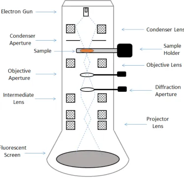
3.2.2 Transmission Electron Microscopy . . . 41
3.2.3 Imaging Modes . . . 45
3.2.4 Atomic Force Microscopy . . . 46
3.2.5 Secondary Ion Mass Spectroscopy . . . 47
3.2.6 X-Ray Photoelectron Spectroscopy . . . 48
3.3 Fabrication . . . 51
3.3.1 Optical Lithography . . . 52
3.3.2 Deposition Techniques . . . 52
3.4 Electrical Characterisation . . . 55
3.4.1 Cyromagnetic Systems . . . 56
3.4.2 Hall and Resistivity Measurements . . . 58
3.4.3 Sources of Error . . . 63
3.5 Electrical Spin Transport Measurements . . . 64
3.5.1 Hanle Measurements . . . 64
Chapter 4 Spin-Orbit Interaction in p-Type Quantum Wells 68 4.1 Introduction . . . 68
4.2 Ge/SiGe Heterostructure and Material Characterisation . . . 69
4.3 Magnetotransport Measurements . . . 77
4.3.1 Fabrication . . . 77
4.3.2 Transport Measurements and Parameters . . . 78
4.3.3 Parallel Conduction . . . 81
4.4 Evidence of Weak Anti-localisation in Low Field Magneto-Resistivity 83 4.5 Summary . . . 91
Chapter 5 Optimisation of Tunnel Barrier Fabrication on Ge 93 5.1 XPS Study of Annealed Ferromagnet/Oxide Films on Ge . . . 94
5.2 Electrical Properties of Ferromagnet/Oxide Tunnel Contacts . . . . 111
5.2.1 Fabrication of TLMs . . . 112
5.2.2 HR-X-TEM Analysis of Oxide Barriers . . . 113
5.2.3 Current-Voltage Characteristics and Contact Resistance . . . 116
5.3 Summary . . . 125
Chapter 6 Spin Lifetime Measurements in Ge 127 6.1 Material Characterisation . . . 127
6.2 Device Fabrication . . . 128
6.3 NiFe/Al2O3/Ge Contact Quality . . . 132
6.4 Electrical Hanle Measurements . . . 133
6.4.1 Experimental Setup and Methodology . . . 133
6.4.2 Electrical Measurements in Sample A and B . . . 134
6.4.4 Spin Signal/Accumulation . . . 144
6.5 Summary . . . 153
Chapter 7 Summary 155
List of Tables
1.1 A table of spin lifetimes and diffusion lengths obtained via electrical
measurements for different semiconductors at 300 K [9][10][11]. . . . 5
2.1 A table containing the basic material and transport properties of
common bulk semiconductors at 300 K [37][41]. . . 17
4.1 A summary table of SO-strengths and transport parameters in various
2DHG systems. * denotes values calculated using the parameters
given in the publication. . . 89
List of Figures
1.1 Density of states for non-magnetic (NM) transition metals (left) and
FM transition meals (right). . . 2
1.2 A FM/NM/FM junction (the magnetisation of FM1 and FM2 can be
parallel or antiparallel) as described by the a simple resistor model.
The size of the resistors indicate the degree of resistance. Adapted
from [23]. . . 6
1.3 Schematics for the operation of a spin-FET. In this case a zero gate
voltage corresponds to a low resistive ’on’ state. . . 10
2.1 A diagram of the diamond cubic unit cell, generated in the Crystal
Maker program. . . 14
2.2 Ge (left) and Si (right) band structure. . . 15
2.3 A diagram demonstrating compressive and tensile strain. . . 18
2.4 A qualitative schematic on the effect of compressive and tensile strain
on the band structure of Ge. . . 19
2.5 A diagram of the SO-effective magnetic field BSO on an electron
travelling at velocityν. The dotted red line traces the precession of
spin due toBSO. . . 20
2.6 The effective magnetic field direction for a given in plane wave vector
for the case of a pure linear Rashba system (left) and a pure cubic
2.7 A diagram showing the density of states in a magnetic field for ideal
d-like Landau levels (left) and Lorentzian like Landau levels due to
scattering (right), adapted from [55]. . . 25
2.8 An electron backscattering after undergoing a series of scattering
events forming a closed loop. The closed loop that results in back
scattering can be described by two separate partial electron waves
forming the loop in opposite directions. . . 27
2.9 Typical shapes of MR curves exhibiting WL (left) and WL/WAL
(right). The area of the right curve within the red dotted lines show
the positive MR when WAL is dominant in low fields. . . 29
2.10 The temperature dependence on the resistance for an Mg film
ex-hibiting WL (top) and Mg/Au film with WAL (bottom), taken from
reference [68]. . . 32
3.1 A simplified schematic of a CVD during growth. . . 35
3.2 A simplified diagram of a typical x-ray diffractometer set up. . . 37
3.3 A diagram revealing the accessible Bragg reflections for a (001) grown
crystal. The arrows indicate the scan movements for shifting values
ofω,2θand ω/2θ. Adapted from [73]. . . 39
3.4 An illustration of (004) and (224) RSMs of a Ge quantum well strained
to a graded SiGe buffer. The SiGe peaks with Ge concentrations such
that x>y are fully relaxed and thus positioned between the relaxed Si
and Ge peaks. The strained Ge quantum well peak is fully strained
to the Si1-yGey and thus shifts to matchax and whilst increasing az. 40 3.5 A simplified schemaic of a TEM column. . . 44
3.6 A simplified AFM set up. . . 46
3.8 A demonstration of a negative process typically used for metal contact
deposition and positive lithography process used for defining a mesa. 53
3.9 A simplified diagram of DC sputtering deposition. The insert shows
the ejection of a target atom after the impact of an ion. . . 55
3.10 A simplified diagram of a pulse tube refrigerator, the compressor is
replaced by a piston for explanation purposes. . . 56
3.11 A simplified diagram of the Heliox AC-V multi-stage CCC, adapted
from the Oxford Instruments operators manual. . . 57
3.12 A schematic diagram of the Hall effect. The perpendicular magnetic
field induces a Lorentz force which causes charge carriers to
accumu-late at the edges of the bar, thus producing a Hall voltage given here
asVxy. . . 59
3.13 A simple six arm Hall bar set-up for magnetoresistivity (top) and
Hall (bottom) measurements. . . 62
3.14 A VdP square magnetoresistivity (left) and Hall (right) measurement
set-up. . . 62
3.15 An illustration of a TLM device (left) and a typical resistance vs.
contact separation plot. . . 64
3.16 An example of a local (top) and non-local (bottom) Hanle set-up.
The grey contacts represent ohmic non-magnetic contacts where as
the yellow and red stacks are FM tunnel contacts. . . 66
4.1 An example band diagram for a modulation doped Ge/Si1−xGex
4.2 (a)A cross-sectional diagram of the sample. (b) The cross-section
of the sample as seen at 5kX magnification in the straight through
beam condition in TEM. (c) The full sample as seen in the (220) DF
condition emphasizing the dislocations in the buffer regions. (d) The
QW region in the (004) condition. . . 71
4.3 Top: SIMS depth profile for Si and Ge concentrations throughout the
heterostructure. Bottom: Si Ge concentrations in the top 300 nm of
the structure with B concentration (violet) on the right axis. . . 73
4.4 Symmetrical (004) and asymmetrical (224) RSM scans of the sample. 74
4.5 A 50mm×50mm AFM scan (left) of the sample displaying the crosshatch pattern and a line profile (right) taken through the centre (left to
right) of the scan. . . 76
4.6 Valence energy band diagram (blue) and hole carrier concentration
(red) as given by self-consistent Poisson-Schr¨odinger simulation at
4 K. EHH corresponds to the filled HH3 energy levels in the Ge QW,
at this temperature, the LH energy levels remain unoccupied. . . 76
4.7 The Hall bar type device fabricated and used in experiments. . . 77
4.8 Top: Temperature dependence of sheet resistivity (blue) and Hall
coefficient (red) for the sample. Bottom: Temperature dependence of
Hall sheet carrier density (blue) and Hall mobility (red). . . 80
4.9 A plot of sheet MR displaying SdH oscillations at high fields and
low fields (inset) for 0.388 K. Anomalous SdH peaks that suggest a
contribution from the presence of a parallel conduction layer are
in-dicated by red arrows and the blue arrows in the inset mark the first
4.10 Low-field magnetoresistivity in the temperature range of 0.44 K-13.2 K,
with curves offset for clarity. The positive magnetoresistivity at the
smallest fields indicates a presence of WAL, the inset shows the
pos-itive MR at 1.9 K at the lowest fields. . . 84
4.11 The low field MR at 2.9 K (left) and the quantum conductance
cor-rection, ∆σ = 1/ρxx(B) −1/ρxx(0) as a function of B/Btr(right).
Btr is much smaller than the width of the WAL feature as well as the
magnet’s minimum field. . . 87
4.12 A simulation of the normalised SdH correction in our sample using
equation 2.14 and calculated parameters. . . 91
5.1 A schematic of the type of structures used in the XPS annealing
studies for FM/Ge and FM/Oxide/Ge stacks. . . 95
5.2 The fitted XPS spectra (TOA 90◦) curves for the Ge 3d peaks for
annealed NiFe on Ge (left) and the calculated Ge concentration as
a function of annealing temperature (right). The inset shows the
various Ge and GeOx (spin-split) peaks used in the fitting at 400◦C. 96
5.3 Ni and Fe concentrations as a function of annealing temperature (left)
and the percentage of oxidised Ni and Ge, compared to their pure
elemental composition. . . 97
5.4 A plot of the measured XPS spectra annealed after an hour at 350◦C,
including the fitted components for Ge 3d (top), Ni 3p (centre) and
Fe 3p (bottom) peaks. . . 99
5.5 A plot of Ge, Ni and Fe concentrations against annealing time for the
5.6 The Ni/Ge XPS spectra at 30◦C, 200◦C and 350◦C, 1 hour into
an-nealing (offset for clarity). Inset: A plot of Ge and Ni (combined
ele-ment and oxide) concentrations against annealing time for the Ni/Ge
stack at 350◦C. . . 101
5.7 The Ni/MgO/Ge XPS spectra at 30◦C, 200◦C and 350◦C, 1 hour
into annealing (offset for clarity). Inset: A plot of Ge, Ni (combined
element and oxide) and MgO concentrations against annealing time
for the Ni/MgO/Ge stack at 350◦C. . . 102
5.8 Top: The Ni/Al2O3/Ge XPS spectra at 30◦C, 200◦C and 350◦C
1 hour into annealing (offset for clarity). Bottom: A plot of Ge,
Ni (combined element and oxide) and Al2O3 concentrations against
annealing time for the Ni/Al2O3/Ge stack at 350◦C. Gaps in the
concentration are due to corrupt scan files. . . 103
5.9 Top: A plot of Ge, Ni, Fe (combined element and oxide) and Al2O3
concentrations against annealing time for the Ni/Al2O3/Ge stack,
at 475◦C. The blue shaded reason covers the time periods in which
atomic concentrations appear to be stable, reflecting ratios consistent
with intact FM/Barrier stacks. . . 105
5.10 A diagram of the type of structures used in the MgO thickness XPS
annealing studies. . . 106
5.11 XPS survey spectra for Ge samples 1, 2 and 3. . . 107
5.12 XPS survey spectra for Si samples 1, 2 and 3. . . 108
5.13 A X-TEM micrograph of Ge sample 1. The MgO/NiFe/Pd sputtered
layers have diffused into the bulk forming a 100-120 nm layer. The
uniformity of contrast in this upper most layer suggests that this
5.14 HR-X-TEM of Ge sample 2, showing the NiFe/MgO/Ge stack. The
Ge appears to be fully crystalline, whilst multiple crystalline domains
are visible in the NiFe. The MgO layer is atomically smooth at both
interfaces, with some areas of the MgO appearing to have some
or-der (noticeably on the right side of the micrograph) suggesting the
beginning of a transition into a polycrystalline phase. . . 110
5.15 HR-X-TEM of Ge sample 3, in the ST-condition (top) and (004)
DF-condition. The MgO barrier remains intact and uniform post
annealing, the Pd/NiFe layer appears as a single polycrystalline layer.
In diffractive mode the areas of the MgO is visible due to areas of
crystallinity. . . 111
5.16 Top: An optical image of a TLM and CTLM device. The deformed/large
contacts on the left side of the TLM device is a result of the thinner
areas of patterned resist bending or lifting off completely. Bottom:
Cross-sectional schematics of the TLM contact/mesa structure for
both FM-tunnel contacts (left) and FM-metallic contacts (right). . . 113
5.17 HR-X-TEM micrograph images in the straight through condition of
a Ti/Ni/MgO stack e-beam evaporated on Ge/Si. Left: 8k
magni-fication showing the complete structure. Mismatch dislocations are
localised at the Si/epitaxial Ge interface. Upper Right: 60k
magnifi-cation of the evaporated material, the MgO layer is visible as a thin
uniform white line. Bottom Right: 100k magnification at the MgO
interface, measuring at a total thickness of 1.4 nm. The dark edge
5.18 HR-X-TEM micrograph images in the straight through condition of a
Ti/Ni/Al2O3 stack e-beam evaporated on Ge/Si. Left: 80k
magnifi-cation at the surface of the Ge sample. The surface of the evaporated
Ni appears to be rough, with the deposited Ti conforming to the
Ni morphology. At this magnification, the Al2O3 is fairly uniform
in thickness. Right: 500k magnification at the oxide interface with
atomic resolution. The Ge is fully crystalline, whilst the Ni layer
con-tains multiple orientations of crystal order. The Al2O3 is amorphous
and has a thickness of∼3 nm. . . 115 5.19 I-V characteristics of CTLM contacts with 32mm separation for Ti/Ni
(top right) and Ti/Ni/Al2O3 with oxide thicknesses 1.5 nm, 3 nm,
5 nm (top right, bottom left, bottom right respectively) on n-Ge.
Multiple measurements for each device is plotted, with some devices
showing fluctuations in I-V characteristics. . . 117
5.20 Resistance as a function of oxide thickness for the CTLM contacts
with 32mm separation for Ti/Ni/Al2O3 on n-Ge. The resistance was
extracted by fitting a straight line at low voltages. Larger errors
de-note contacts with significant variations in repeat measurements, the
red circle marks the value ofRwhen the anomalously large resistance
was measurement is included. . . 118
5.21 TLM plots of Ni/Al2O3 and NiFe/Al2O3 contacts on n-Ge. The size
of error bars indicate the degree of variability between repeat I-V
measurements. . . 120
5.22 TLM plots of Ni/MgO contacts on n-Ge. The size of error bars
indicate the degree of variability between repeat I-V measurements. 121
5.23 Contact RA against oxide thickness for the Ni/Al2O3and NiFe/Al2O3
5.24 An extreme example of resistance switching between and during
re-peat I-V measurement sweeps for an Ti/Ni/Al2O3 on n-Ge CTLM
contact (32mm separation). The green and black arrows indicate
points at which the contact experiences a shift in I-V characteristic
during a measurement. . . 123
6.1 A 50mm×50mm AFM scan (left) of the sample and a line profile (right) taken through the centre (left to right) of the scan. . . 128
6.2 a)A diagram of the Hanle device design as viewed from above. b)Optical
micrograph of the spin tunnel contacts of a fabricated device located
in the centre of the mesa. c) A cross-sectional diagram of the device
set up in a local 3T measurement orientation. . . 129
6.3 Plots of carrier concentration (n) and Hall mobility (µH) between
20 K and 290 K, measured from VdP squares for sample A (top) and
sample B (bottom). . . 131
6.4 X-TEM micrographs of a Au/Ni/Al2O3 contact. The following
im-ages are provided; contact/sample in the (004) DF (a) and BF (b)
at×80k magnification, ×10k magnification of the whole structure in ST condition (c) and×500k magnification in the ST condition in the vicinity of the barrier (d). . . 132
6.5 A plot of the voltage drop across the FM contact and the reference
contact as a function of field for sample A. A negative (positive) bias
corresponds to spin injection (extraction). . . 134
6.6 Examples of Hanle signals measured in sample B for two adjacent
devices at similar temperatures and bias currents. The measured
data is plotted as black circles, whilst the resulting fit is given as
a red line. Device 1 (left) appears to be much higher quality with
6.7 Plots of the anomalous behaviour in sample B, found when using
positive (left) and negative (right) bias. Red (black) circles denote
data points measured in a positive (negative) field sweep. The
be-haviour associated with positive bias appeared to shift segments the
curve vertically, the amount of which varied and did not necessarily
occur for the same region of field when reversing the sweep direction.
In contrast, negative bias produced a second vertically off set curve
which consisted of data points from both sweep directions. . . 137
6.8 A Hanle curve measured at 10 K for sample A, with IBias =-200 nA.
Data points are represented by circles and the resulting Lorentzian
Hanle fit is plotted as a solid red line. . . 139
6.9 A plot of the Hanle curve measured at different temperatures for
IBias=-200 nA for sample A. . . 139
6.10 The extractedτsvalues for sample A as a function of temperature for
both spin injection (red) and extraction (black). . . 140
6.11 A relatively low noise plot of the apparent Hanle signal measured in
sample B, device 1 at 280 mK with a bias current 100 nA. . . 142
6.12 Temperature dependence of τs extracted from selected Hanle curves
with minimal noise and anomalous behaviour in sample B, device 1
for different bias currents. . . 143
6.13 A plot of the RsA product as a function of temperature for spin
injection (red) and extraction (black) in sample A. . . 146
6.14 Plots of ∆V(0) (top) andRsA(bottom) for sample A, with different
bias currents at 22 K, the inset shows a constantτs for all bias currents.146
6.15 Temperature dependence ofRsAextracted from selected Hanle curves
with minimal noise and anomalous behaviour in sample B, device 1
6.16 Plots of sample B device 2 Hanle curves, measured at a range of
temperatures for bias current -200 nA. As temperature is increased,
the Lorentzian curve amplitude decreases corresponding to a decrease
in spin accumulation, for temperatures above 20 K no visible spin
signal is observed. . . 150
6.17 Plots of sample B device 2 Hanle curves, measured at 3 K for different
bias currents. The spin signal increases with bias current, above
this, the noise become worse and the signal begins to drop until no
noticeable signal can be observed at -400 nA bias. Above this limit,
Acknowledgments
This thesis would not have been complete without the support of a number of people
over the past four years. I would like to thank my supervisors Prof. David Leadley
and Dr. Maksym Myronov for giving me the opportunity to carry out this Ph.D.
and for their general guidance throughout my project.
Next I would like to thank Dr. Maksym Myronov once again for growing
me the samples that have formed the basis my project. As for the remainder of
the Nano-Silicon group, I am grateful for the guidance given to me by Dr. Chris
Morrison on the subject of electrical measurements and spintronics. I would also
like to thank Dr. Vishal Shah, Dr. Stephen Rhead and Dr. John Halpin for teaching
me all the material techniques I have used in this project and of course Dr. Alan
(Turbo) Burton, as without him I’m sure none of the equipment would have worked
for long.
As for the members who were students whilst I was here; John, Dave, Olly,
Phil, Gerard, James and Cat, I have enjoyed all the fun times weve had in the offices,
my Ph.D. and lunch breaks would have been dull without them.
I also would like to thank Leanne, who helped me keep going and supported
me, particularly in the last months of writing
Finally I would like to thank my family, without them, I would not have had
Declarations
The work described in this thesis was carried out either by the author himself,
or under the direction/supervision of the author at the Department of Physics,
University of Warwick, with the exception of the following cases
• RP-CVD growth of the semiconducting material was carried out by Dr. Maksym Myronov.
• Collection some XPS spectra (as stated in the text), by Dr. Marc Walker.
• Collection of SIMS data carried out by Evans Analytical Group.
Publications
0.1
Publications
0.1.1 Publications Cited in This Thesis
• Reference [58]
C. Morrison, J. Foronda, P. Wisniewski, S. D. Rhead, D. R. Leadley, M.
Myronov,
Evidence of strong spin-orbit interaction in strained epitaxial germanium,
Thin Solid Films 602, 84 (2016).
• Reference [83]
J. Foronda, C. Morrison, J. Halpin, S. D. Rhead , M. Myronov,
Weak antilocalization of high mobility holes in a strained Germanium
quan-tum well heterostructure,
Journal of Physics-Condensed Matter 27, 022201 (2015).
• Reference [82]
C. Morrison, P. Wisniewski, S. D. Rhead, J. Foronda, D. R. Leadley, M.
Myronov,
Observation of Rashba zero-field spin splitting in a strained germanium 2D
hole gas,
Applied Physics Letters 105, 182401 (2014).
• Reference [36]
V. A. Shah, D. R. Leadley,
An extremely high room temperature mobility of two-dimensional holes in a
strained Ge quantum well heterostructure grown by reduced pressure chemical
vapour deposition,
Japanese Journal of Applied Physics 53, 04EH02 (2014).
0.1.2 Publications Not Cited In This Thesis
• M. Myronov, C. Morrison, J. Halpin, S. Rhead,J. Foronda, D. R. Leadley, Revealing high room and low temperatures mobilities of 2D holes in a strained
Ge quantum well heterostructures grown on a standard Si(001) substrate,
Solid-State Electronics 110, 35 (2015).
• P. J. Newton, J. Llandro, R. Mansell, S. N. Holmes, C. Morrison,J. Foronda, M. Myronov, D. R. Leadley, C. H. W. Barnes,
Magnetotransport in p-type Ge quantum well narrow wire arrays,
Applied Physics Letters 106, 172102 (2015).
0.2
Conference Participation
• C. Morrison,J. Foronda, M. Myronov,
The Rashba Spin Orbit Interaction in Ge Quantum Wells
IOP Magnetism, Sheffield,UK (2016).
Ge QW Heterostructure,
2014 7TH International Silicon-Germanium Technology and Device Meeting
(ISTDM), Singapore, SINGAPORE (2014).
• M. Myronov, C. Morrison, J. Halpin, S. Rhead,J. Foronda, D. R. Leadley, Revealing the high room and low temperature mobilities of 2D holes in a
strained Ge quantum well heterostructures grown on a standard Si(001)
sub-strate,
2014 7TH International Silicon-Germanium Technology and Device
Meet-ing(ISTDM), Singapore, SINGAPORE (2014).
• C. Morrison, M. Myronov, J. Foronda, C. Castelerio, J. Halpin, S. Rhead, D. R. Leadley,
Quantum Transport of a High Mobility Two Dimensional Hole Gas in a
Strained Ge Quantum Well,
2014 7TH International Silicon-Germanium Technology and Device Meeting
(ISTDM), Singapore, SINGAPORE (2014).
• C. Morrison, M. Myronov, J. Foronda, S. Rhead, D. R. Leadley,
Transport Properties of Unintentionally Undoped Ge Quantum Well
Het-erostructure,
International Conference on the Physics of Semiconductors, Austin, Texas,
USA (2014).
• C. Morrison, J. Foronda, M. Myronov, S. Rhead, D. R. Leadley, P. Wis-niewski
Zero Field Spin Splitting in a High Mobility Ge 2D Hole Gas,
International Conference on the Physics of Semiconductors, Austin, Texas,
• C. Morrison, J. Foronda, M. Myronov, D. R. Leadley, P. Wisniewski Observation of Rashba Spin Splitting in a Ge 2D Hole Gas
Abstract
The field of semiconductor spintronics is relatively underdeveloped when compared to its metallic counterpart which has found great success in the computer storage industry in hard disk drive head technology and to a lesser extent non-volatile and robust (M)RAM. The use of semiconductors in spintronics is promising with the ability to modulate spins via a gate controlled spin-orbit interaction al-lowing for spintronic logic and computation devices. Combining this with dilute ferromagnetic semiconductors, which have been suggested as a base for semicon-ductor MRAM, it may even be possible to integrate MRAM and logic into a single chip to allow for further miniaturisation of devices. In this thesis we look into the suitability of Ge as a platform for semiconductor spintronics verses other popular alternatives such as Si and GaAs.
The first section of this thesis looks at evidence of a strong spin-orbit inter-action in low temperature magnetoresistance curves measured in a high mobility (777,000 cm2V−1s−1) Ge 2DHG. Despite the lack of beatings in Subnikov de Haas oscillations, which often serves as a indicator of a strong spin-orbit coupling, weak antilocalisation like behaviour is seen at low fields. The spin splitting energy ex-tracted from the weak antilocalisation and found to be 0.8 meV with a Rashba parameter of 3.2×10⁻²⁸eVm3. The spin split energy is comparable to other Ge and III-V 2DHGs, however the Rashba parameter is in fact higher, which we believe is attributed to the high level of remote doping.
The second section focuses on the treatment of ferromagnet/oxide spin tunnel contacts on Ge deposited by evaporation or sputtering, both of which are common in industrial scale fabrication. Annealing XPS studies are conducted on these con-tacts to examine the temperature limits at which annealing treatments can be done before contacts degrade. Transition line measurements are also examined to look at the electrical characteristics of the deposited contacts.
Abbreviations
– 2DEG: 2-Dimensional Electron Gas
– 2DHG: 2-Dimensional Hole Gas
– 3T: 3-Terminal
– 4T: 4-Terminal
– AF: Anti-Ferromagnetic
– AFM: Atomic Force Microscopy
– BF: Bright Field
– BIA: Bulk Inversion Asymmetry
– CCC: Closed Cycled Cryostat
– CVD: Chemical Vapour Deposition
– DF: Dark Field
– DP: Dyakonov-Perel
– EY: Eliot-Yafet
– FET: Field Effect Transistor
– FIB: Focused Ion Beam
– FTT: Fast Fourier Transform
– GMR: Giant Magneto-Resistance
– HH: Heavy Hole
– HR: High Resolution
– LH: Light Hole
– LRG: Linearly Reverse Graded
– MC: Magnetoconductivity
– MOSFET: Metal-Oxide-Semiconductor-Field-Effect-Transistor
– MR: Magnetoresistivity
– MRAM: Magnetic Random Access Memory
– MTJ: Magnetic Tunnel Junction
– NM: Non-Magnetic
– Ox: Oxide
– PTR: Pulse Tube Refrigerator
– QW: Quantum Well
– RA: Resistance Area product
– RcA: Contact Resistance-Area product
– RsA: Spin Resistance-Area Product
– RF: Radio Frequency
– RMS: Root Mean Square
– RSM: Reciprocal Space Map
– RTA: Real Time Annealing
– SC: Semiconductor
– SdH: Shubnikov de Haas
– SEM: Scanning Electron Microscopy
– SHE: Spin Hall Effect
– SIA: Structural Inversion Asymmetry
– SIMS: Secondary Ion Mass Spectroscopy
– SO(I): Spin Orbit (Interaction)
– TEM: Transmission Electron Microscopy
– TLM: Transmission Line Measurements
– TMR: Tunnelling Magneto-Resistance
– TOA: Take-Off Angle
– TSP: Tunnelling Spin Polarisation
– UHV: Ultra-High Vacuum
– UV: Ultra Violet
– VdP: Van der Pauw
– VS: Virtual Substrate
– WAL: Weak Anti-Localisation
– WL: Weak Localisation
– XPS: X-Ray Photoelectron Spectroscopy
Chapter 1
Introduction
1.1
Spintronics
The digital age has thrived on technology that employs the transport and
manip-ulation of charge carriers for the transfer and processing of information.
Semicon-ductors have been at the centre of computing since the manufacturing of the first
commercial n-p-n bipolar type Si transistor in the mid 1950s to the widely used
metal-oxide-semiconductor-field-transistor (MOSFET). A high resistance in these
transistor devices corresponds to an ‘off’ or ‘0’ state and a low resistance an ‘on’ or
‘1’ state. Spintronics is a branch of electronics which moves away from charge based
transport and focuses on the intrinsic angular momentum (spin) of the carriers. The
spin of electrons/holes can take the values of either +12 or−1
2 and is what gives spins
their magnetic moment (µB) that allows interaction with other magnetic moments
or magnetic fields. The use of pure spin (polarised) currents promises much lower
energies [1].
The field of spintronics was first established in 1988 with the discovery of
gi-ant magneto-resistance (GMR). Initial studies on GMR by two independent groups
Albert Fert et al. [2] and Peter Grunberg [3] involved ferromagnetic (FM) Fe and
Figure 1.1: Density of states for non-magnetic (NM) transition metals (left) and FM transition meals (right).
particular thickness of which allowed the exchange interaction between adjacent Fe
layers to form an antiparallel magnetisation configuration. The application of an
in-plane field causes a significant decrease in resistivity when the magnetisation of
the Fe layers switch from an antiparallel to parallel configuration. This effect is the
result of spin dependant scattering. Resistivity in transition metals originates from
scattering events that cause 4s electrons to scatter into the 3d states. In FM
mate-rials the density of states in the d-band are spin-split such that the minority spins
have more unoccupied states than the majority spins, because of this the minority
spin carriers are more likely to be scattered as they will have velocities smaller than
majority spins for a given energy. In an antiparallel configuration, the majority
carriers that flow from one FM layer to the other become minority spin carriers in
the other and thus are preferentially scattered, leading to the increase of resistance.
In these first two studies, the magnetoresistance (MR) dropped as far as 3% at room
temperature and up to 50% at 4.2 K.
Ferromagnetism arises from the exchange interaction, which causes a spin
splitting in the 3d band of FM metals. The spin dependent splitting leads to an
imbalance of 3d up and down spin states occupied, as demonstrated in Fig. 1.1.
of states at the Fermi level (EF)
P = g↑(EF)−g↑(EF)
g↑(EF) +g↑(EF)
(1.1)
g↑,↓ refers to the density of states for the spin sub-bands. The asymmetry of the spin
up and down density of states atEF results in a partially spin polarised current, as
the 4s and the 3d bands both contribute to conduction in transition metals.
GMR was quickly observed in other multilayer systems such as Co/Ru,
Co/Cr and Co/Cu [4][5]. Studies moved onto using spin valve type structures where
two FM layers were separated by a spacer and the magnetisation of one FM layer
was fixed or pinned using an adjacent AF layer. The sensitivity of GMR in these
types of structures led to the use of GMR-based read heads in hard-disk drives, first
showcased by IBM in 1997, driving storage densities to much higher capacities (by
two orders of magnitudes). The importance of GMR to the field of spintronics and
magnetic storage was recognised in 2007 when Fert and Gr¨unberg were awarded the
Nobel prize for their discovery. Storage densities were later surpassed with the
im-plementation of tunnelling magnetoresistance (TMR) type heads. This effect stems
from GMR in spin valves, with the difference of using a tunnel barrier in place of a
NM or AF spacer to from a magnetic tunnel junction (MTJ). Initial measurements
showed much larger MR ratios than typically seen in GMR at 20%, more recent
experiments boast figures as high as 600%.
Apart from hard disk drive read heads, spintronics has also made an impact
in the computing industry in the form of magnetoresistive random-access memory
(MRAM)[6], in which information is stored in FM elements that can be switched
using electric currents (via the spin torque mechanism). FM elements allow
infor-mation to be stored in a non-volatile format, furthermore the promise of high speeds
and storage density, makes it a future candidate for universal memory. Currently
extreme temperatures and durability (resistive to radiation damage) it has found
uses in military and aeronautical industries.
1.2
Semiconductor Spintronics: Introduction and Basic
Concepts
Semiconductor spintronics, in contrast to the metal spintronics discussed above is
a much newer underdeveloped sector of spintronics. This stems from the fact that
conventional semiconductors have no net spin polarization at equilibrium, providing
the need for the injection of spin carriers into semiconductors for spintronic devices.
Spin injection in materials can be performed in a number of different ways. It had
been demonstrated first in GaAs [7] that it was possible to inject spin using
circu-larly polarised light due to GaAs selection rules, other methods also include the spin
pumping of an adjacent FM layer [8]. The two methods however, are not practical
for real world application of spintronic devices, instead it is also possible to inject
spin electrically through the use of a FM electrode.
Once spins are injected into a non-FM material, they will diffuse into the
bulk and over a certain length will lose or ‘forget’ its spin orientation due to the
effects of random magnetic fields or spin changing scattering events (discussed later
in section 2.3). It follows that the degree of spin polarisation in the bulk material
will decay exponentially the further away the spins are from the site of injection.
The characteristic time scale at which this happens is known as the spin relaxation
time,τsand the corresponding length scaleLs(the spin relaxation length) is defined
as L = √Dτs where D is the diffusion coefficient. Ls thus determines the length scale at which a spintronic device can operate. Semiconductors benefit from having
larger values ofLsover metals. Experimentally measuredτsandLsvalues are given
for Si, Ge and GaAs in table 1.2.
n-type p-type
τs (ps) Ls (nm) τs (ps) Ls (nm)
Si 140 230 270 310
Ge 123 830 15 120
GaAs 900 - 320
-Table 1.1: A table of spin lifetimes and diffusion lengths obtained via electrical measurements for different semiconductors at 300 K [9][10][11].
injection has been achieved both optically [12] and electrically in a number of
dif-ferent semiconductor systems, as well as being detected electrically via the Hanle
effect[13][14][15][16][17][18][19][20]. Interesting phenomena such as the spin Hall
ef-fect (SHE) [21] has also been observed in GaAs [22] where spin orbit (SO) related,
spin dependent scattering induces a fully spin polarised current perpendicular to an
applied charge current. Before we discuss semiconductor spintronics further, let us
address some basic concepts.
1.2.1 Spin Injection into Non-Magnetic Materials
Initial discussions of electrical spin injection focused on the concept of diffusive
FM/NM and FM/NM/FM junctions, with the application of a bias voltage between
one FM electrode and the NM layer. The bias voltage effectively raisesEF in the
FM, causing electrons to have higher energies than those at EF in the NM layer
allowing a flow of electrons from FM to NM in order for the electrons to achieve
a lower energy and equilibrium. As g↑(E) 6= g↓(E), an uneven number of up and
down spins flow into NM. Conversely, if the bias is reversed, the chemical potential
in the NM layer is now higher, reversing the flow. g↑(EF) for the FM however is
larger thang↓(EF), thus allowing more↑spins than↓ into the FM and causing the minority↓ spins to accumulate in NM. This is known as spin extraction.
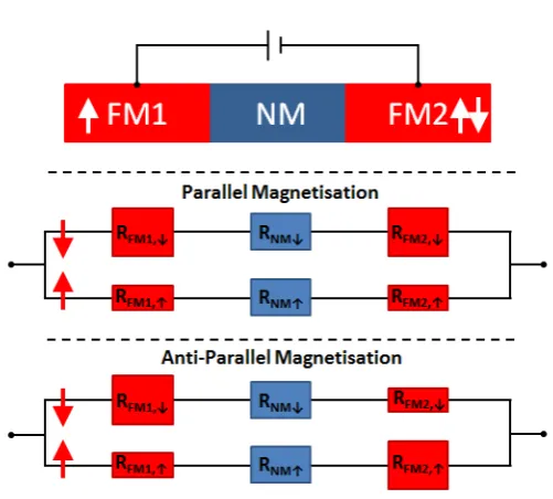
For injection into metals electrical injection is trivial, however a problem
arises when the conductivity of the spin injecting contact material in vastly different
Figure 1.2: A FM/NM/FM junction (the magnetisation of FM1 and FM2 can be parallel or antiparallel) as described by the a simple resistor model. The size of the resistors indicate the degree of resistance. Adapted from [23].
the injected current is very small of the order ∼0.1% [23][24]. This is known as the conductivity mismatch problem and can be derived from the simplified resistor
model where contributions to the current are described as two separate conduction
channels with equal currents for spin↑and↓and each material has a respective spin dependent resistance. This is depicted in figure 1.2. In this discussion we label the
spin dependent resistance for the FM asRF M↑,RF M↓ and the NM layer intuitively
has RN M↑ = RN M↓ = 2RN M. The efficiency of spin injection is defined by the
proportion of spins currents flowing from the FM into the NM
ζ = j↑−j↓
j↑+j↓
(1.2)
where j↑,↓ are the individual current densities and the charge current density is
j = j↑ +j↓. When discussing the behaviour of spins in the spin valve, the spins
defined as
R↑=ρ↑
l
A (1.3a)
R↓=ρ↓
l
A (1.3b)
where ρ↑,↓ are the resistivities of the spin channels and the inverse the spin
con-ductivity σ↑,↓. The resistor model for an FM/NM/FM junction is given in figure
1.2, for both parallel and antiparallel orientations of the FM electrode’s
magneti-sation, the two FM layers have identical magnetic and electrical properties (i.e.
RF M1 = RF M2). When a spin ↑ travels through a FM with opposite sign to the
magnetisation then the resistance RF M↑ is large, if it is parallel the value is small.
We define the effective conductivity polarisation for a particular layer as
βp=
σ↑−σ↓
σ↑+σ↓
(1.4)
which is non-zero in FM and zero in NM. This in combination with the total
resis-tance of the FM, 1/RF M = (1/ρ↑+ 1/ρ↓)Al, equations 1.3a, 1.3b for the FM regions
can be changed to
RF M↑ =
2RF M 1 +βp
(1.5a)
RF M↓ =
2RF M 1−βp
(1.5b)
The total resistance for one channel (R↑, R↓) is just the series resistance of the
spin-dependent current from the three layers. In the antiparallel magnetisation scenario,
the two channels will have equal resistances. As J ∝ 1/R we can write the spin polarisation across the junction as
αp =
R↓−R↑
R↑+R↓
in which in the antiparallel set-upαp is zero. For the parallel set-up the resistances
of the FM electrodes in a particular spin channel are the same and thus R↑ =
2(RF M↑+RN M) andR↓ = 2(RF M↓+RN M), substituting these as well as equations
1.5a, 1.5b we have
αp=
RF M↓−RF M↑
RF M↑+RF M↓+ 2RN M
(1.7a)
αp =βp
RF M
RN M
2
2RF M/RN M+ (1−βp2)
(1.7b)
We can see that the polarisation is dependent onβp and a ratio of the FM and NM
resistances. This result presents one of the larger obstacles for semiconductor (SC)
spintronics and was first pointed out by Schmidt et al [23]. As most conventional
FM materials are metallic, the resistance ratio is very small reducing the efficiency
of spin injection significantly, even with the use of half metals with a spin
polarisa-tion of 100%.
One option to avoid this problem is the use of unconventional ferromagnetic
semiconductors [25] as contact material, however these cannot be deposited as
eas-ily standard FM and often suffer from low Currie temperatures, much lower than
room temperature. Instead Fert and Yaffres found that if the interface resistance of
the FM/SC was larger than the spin resistance of both the FM and SC layer, the
conductivity mismatch problem could be overcome, the proof of this is provided in
[26]. This was also highlighted by Rashba at a similar time [27], suggesting the use
of a tunnel barrier and to a lesser extent a Schottky barrier to achieve this effect.
Since then, there have been a large number of studies in III-Vs, Si and Ge where
efficient spin injection has be achieved through spin tunnel contacts using either
in-sulating (oxide) tunnel barrier such as MgO and Al2O3[13][14][15][16][17][28][29][30]
1.2.2 Spin Modulation
In addition to spin flip scattering, the orientation of a spin can change with time
when in the presence of a magnetic field. If the magnetic moment of an electron (µB)
has a component perpendicular to an external magnetic field (B), the magnetic
moment will experience a torque (Γ) perpendicular to both the moment and B
(Γ = µB ×B) causing the moment or spin or precess about the field (Larmor Precession). The rate of the precession is given as
Ω=µBgB/¯h (1.8)
where g is the Lande g-factor. Although Larmor precession is another source of
spin relaxation, it can also be used to modulate spin, this can be achieved more
efficiently using the spin orbit interaction (SOI). The SOI was initially realised for
electrons orbiting around the electric field of a positive nucleus, intuitively using
heavier elements results in a larger SO due to the larger field of the nucleus. The
strength of the SOI in semiconductors however are not limited to their ‘Z’ value, but
can also be introduced by forming a structural electrical field (Rashba SOI) such
as one found in asymmetrical quantum wells [31]. Further tuning is possible simply
by introducing a gate voltage to adjust the electrical field in the material. Further
details will be discussed in section 2.2.1.
Electrical tuning of the SOI, forms the core concept for the spin-analogue
of the field effect transistor (FET) proposed by Datta and Das in 1990 [32] for use
in spin based computing logic. The proposed device consists of a FM source and
drain used to inject a spin polarised current separated by a gated a 2-dimensional
hole or electron gas channel, as depicted in figure 1.3. Spins traversing the channel
precess due to the effective magnetic field from the SOI. The SOI can be tuned such
that the spins arriving at the drain can either the have the same orientation as it
Figure 1.3: Schematics for the operation of a spin-FET. In this case a zero gate voltage corresponds to a low resistive ’on’ state.
orientation. If spins have the same orientation as the magnetisation of the drain,
the resistance across the contacts is low, if the spins have the opposite orientation,
then the resistance across the transistor is high. The gate voltage is used to switch
the transistor on and off by modulating the SOI via a gate voltage.
The demonstration of both semiconductor based MRAM and spin logic would
be a large development in the field of spintronics, giving rise to the possibility of
unifying both storage and logic capabilities onto a single chip. The combination of
the two functions onto a single chip is becoming more attractive with the
miniatur-isation of technology, with the additional benefit of lower power consumption when
compared to current mobile technology.
1.2.3 Motivation and Thesis Outline
A significant portion of research in semiconductor researched has focused on III-V
materials such as GaAs [11][22] and InGaAs [33]. Being a direct bandgap material,
however other advantages also include large SOI and large mobilities for large spin
relaxation lengths. A major disadvantage of using non-centrosymmetric
semicon-ductors (group III-V and II-VI), is the presence of the Dresselhaus SOI due to the
inversion asymmetry of these materials [34]. This SOI effect is not tuneable like the
Rashba interaction and can cause additional spin relaxation. The Dresselhaus SOI
will be discussed further in section 2.2.1
As for group IV materials, Si has also been popular, as its wide spread use
in the electronics industry has meant Si processing is well established and thus an
Si platform is desirable to industry. Its relatively low mass and in turn weak SOI,
implies long spin relaxations times and although some cite this as an advantage, it
also sacrifices performance in spin modulation devices.
In this thesis I examine the feasibility of using Ge as a platform for
ductor spintronics. Ge alternately combines the advantage of both V-III
semicon-ductors and Si. As a heavier element than Si the SOI interaction in Ge is larger, but
does not suffer from the Dresselhaus SOI that III-Vs have. Furthermore as a group
IV material it remains compatible with the widely established processing techniques
and high mobilities have routinely been achieved [35][36] by staining 2D Ge layers,
approaching III-V values.
In chapter two I outline the basic properties of Ge and Si as well as the
con-cepts required to understand later discussions on SOI and SOI-related phenomena.
Experimental techniques along with their associated analysis techniques employed
during the investigation will be discussed in chapter three. Chapter four studies the
Rashba SOI of a highly strained Ge quantum well (QW) through low temperature
magnetoresistance measurements. Later chapters are dedicated to investigating the
effectiveness of spin tunnel contacts, namely using Ni, NiFe, Al2O3 and MgO
fab-ricated with common deposition tools. First in chapter five, an annealing study
using x-ray photoelectron spectroscopy, looks at the thermal stability of these
characterisation of as deposited tunnel contacts. Chapter six focuses on the
mea-surement of the spin lifetime in n-Ge using the as deposited Ni/Al2O3. Following
these results chapters a summary of the investigation is given and suggestions on
Chapter 2
Theoretical Discussion
2.1
Properties of Silicon and Germanium
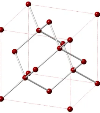
Si and Ge are group-IV semiconductors with a diamond cubic crystal structure
illustrated in figure 2.1. The basic properties of Si, Ge and other semiconductors
are given in table 2.1.1. With a Z number of 14, Si has a smaller lattice parameter of
aSi=5.431 ˚A with Ge ataGe=5.658 ˚A [37]. Both of these elements can be combined to form an alloy (of the same structure) Si1-xGex where x is the ratio of Ge in the
material which can take the values 0< x <1. The resulting lattice parameter of the
Si1-xGex at a particular temperature is determined by Vergard’s law (essentially a
weighted average of the two lattice parameters) defined as
aSi1−xGex = (1−x)·aSi+x·aGe−0.00273x(1−x) (2.1)
where aGe and aSi are the lattice constants at the desired temperature and the
latter term is a correction factor initially proposed by Kasper and later modified by
Salvador et al after a linear deviation was discovered from measurements of various
Figure 2.1: A diagram of the diamond cubic unit cell, generated in the Crystal Maker program.
2.1.1 Band Structure of Ge and Si
The band structure of a material describes the possible energies an electron can have
when occupying certain states in a lattice (characterised by the wave vectork), these
are derived by solving the wave functions of electrons in a periodic potential which is
defined by the lattice of atoms/molecules. The band gap of semiconductors is defined
as the energy between the conduction (minima) and valence band (Gmaxima), where
there is forbidden range of energies in which there are no states for electrons to
occupy in the absence of any impurities. Both Si and Ge have indirect band gaps
where the Si conduction band minima is in the [100] direction (known as the ∆
minima) with a band gap of 1.12 eV and the Ge minima occurs in the [111] direction
(L minima) forming a band gap of 0.66 eV. The band diagrams for Si and Ge are
given in Figure 2.2. For Si1-xGex alloys, the band gap decreases in energy from
the Si value down to the Ge value as x is increased. It has been found that for
0< x <0.85, the conduction band minima is Si-like (∆), transitioning to an L
minima for 0.85< x <1 [40].
Figure 2.2: Ge (left) and Si (right) band structure.
to an angular momentum of l = 0, where as the valence bands are p-type (l= 1),
as a consequence the valence band is formed of three bands corresponding to states
with total angular momentum (j = l+s) j = 3/2 where mj = ±3/2,±1/2 (the projection of total angular momentum on an arbitrary axis) and j = 1/2 with
mj =±1/2. At the valence band maxima (k= 0), when ignoring the SOI the three bands are expected to be six-fold degenerate. Due to thes=−1/2 of thej = 1/2 band, the SOI lifts the degeneracy between thej= 3/2 andj= 1/2 bands, inducing
a SO-split energy ∆0 (for which in Ge is ∆Ge0 =0.30 eV and for Si ∆Si0 =0.044 eV)
[37][38]. The shift in the j = 1/2 band has led it to be called the spin orbit-split
band.
The two j = 3/2 bands are known as the heavy hole (HH) and light hole
(LH) bands, due to their effective masses (m∗). The effective mass is used, as the
mass of a carrier is different in a periodic potential than in a vacuum. The effective
mass of a carrier is derived from the curvature of the band it occupies. Close to
the valence band minima, the bands can be considered parabolic taking the form
the effective mass using the following equation
µ= qτtr
m∗ (2.2)
whereq is the carrier charge and τtr is the transport scattering time, the inverse of
which is the summation of the scattering rates of the various scattering mechanisms
(Matthiessen’s rule). The lower m∗ for carriers in bulk Si in comparison to Ge
accounts for the higher mobilities in bulk Ge.
From the values ofm∗ in table 2.1.1, it can be seen why Si suffers from lower
mobilities than Ge.
2.1.2 Strain Effects in Germanium
The growth of a material onto a substrate with the same crystal structure and
dif-ferent lattice parameter can lead to the top-most layer becoming strained, where
the atoms/molecules of the top-most layer attempt to match the positions of the
corresponding atoms/molecules in the layers below. When Si, Ge and Si1−xGex alloys grown in the (001) direction are under strain, the unit cell deforms
tetrago-nally, such that a reduction in in-plane parameters (ax, ay) leads to an increase in
out-of-plane parameter (az). az of a strained sample grown on a (001) substrate can
be calculated with the following equation
az=abulk+ 2c11
c12
(abulk−ax) (2.3)
where c11 and c12 are the elastic moduli. Figure 2.3 illustrates the type of strain
produced when growing onto substrates with differing lattice parameters. If the
epitaxial layer is strained to a substrate with a larger lattice parameter, the epitaxial
layer will be under tensile strain, conversely if the substrate has a smaller lattice
Figure 2.3: A diagram demonstrating compressive and tensile strain.
The strain (ε) of an epitaxial layer with respect to the substrate is given by
ε= asubstrate−alayer
asubstrate
(2.4)
The lattice mismatch for Ge and Si is 4.17% meaning Ge grown on Si will be
compressively strained (ε=−0.0471). As stated earlier Si1-xGex alloys can have a
lattice parameter that can take intermediate values between that of Si and Ge by
varyingx, this can be used to achieve different levels of compressive biaxial strain in
Ge layers (−0.0417> ε >0) by growing crystalline Ge on Si1-xGexvirtual substrates
(VS) [42][43]. Inversely, it is possible to produce tensile strained Si using Ge or
Si1-xGex VS and tensile strained Ge using GexSn1-x VS. The amount of material it
is possible to strain is however limited, above a critical thickness misfit dislocations
form to release the strain in a layer, this thickness will decrease as the mismatch
between lattice parameters increase. For Ge on Si, the critical thickness has been
Figure 2.4: A qualitative schematic on the effect of compressive and tensile strain on the band structure of Ge.
Strain Effects On Bands and Carrier Transport
Strain engineering has routinely been used to enhance the transport properties in
2DEG and 2DHG [35][36][43]. The introduction of strain into a semiconductor often
results in the deformation of bands (reducing parabolicity and changingm∗) and a
shift in energy. A qualitative schematic of strain effects on the Ge band structure
is given in figure 2.4. Inducing compressive strain shifts the HH band up in energy
and decreases m∗HH (making it more LH-like) whilst lowering the LH band and
increasing m∗LH. Due to the shifts in LH and HH bands, the valence band at the
G-point becomes only two-fold degenerate and only the HH-band is occupied for
low hole concentrations, furthermore the lowering of m∗HH enhances µ (as seen in
equation 2.2). In the case of tensile strain the inverse happens where the LH band
reduces inm∗ and rises above the HH band, which increases inm∗. The result is the
occupation of only the LH band, again increasingµ due to the overall reduction of
m∗ (due to both the lack of HH and band deformation). In terms of the conduction
valley shifting at a faster rate than the L valley, these valleys move in the opposite
direction for compressive strain.
2.2
Spin-Orbit Interaction
The SOI is a relativistic effect in which moving spins interpret electric fields as
effective magnetic fields and forms the basis of a number of interesting phenomena
in both spintronics and quantum computing [45]. Its initial discovery was used
to describe the interaction between the spin and orbital angular momentum of an
electron. In the rest frame of the nucleus, the electron can only see the electric field of
the positive atom ion. In the stationary reference frame of the electron, the charged
nucleus appears to be travelling in an orbital motion around the electron, thus
generating a magnetic field perpendicular to the velocity (ν) of the electron/nucleus
and the electric field with magnitude
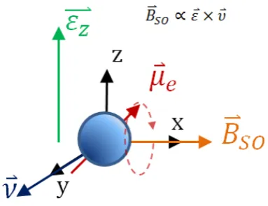
[image:48.595.231.423.518.665.2]BSO= (1/c)E×ν (2.5)
Figure 2.5 illustrates the resulting effectiveBSO from the application of an electric
field to an electron applied perpendicular toν.
Like Zeeman splitting, this effective field leads to a shift/slitting in atomic
energy levels (±µBB). The size of the energy shift is dependent on the intrinsic and orbital angular momentum (s and l) as well as the ‘Z’ (atomic) number of
the nucleus which defines the magnitude of the electric field. This generally means
heavier elements tend to generate larger SO energy shifts than lighter elements.
2.2.1 Rashba and Dresselhaus Spin Orbit Interactions
The SOI felt by conduction electrons or holes due to the positive field of the nucleus
is in reality fairly small due to the masking of the nucleus’ electric field by other
electrons. There are however other sources of the SOI, Dresselhaus first suggested
that crystal structures lacking structural inversion symmetry such as the zinc blende
type crystal that most III-V semiconductors have, will have an additional
contri-bution to the zero field spin splitting [34]. In the case of inversion symmetry, the
spin states are degenerate such that E+(k) = E+(−k) (where + and − refer to
spin up and down) and with time inversion symmetry,E+(k) =E−(−k) (as time
inversion reverses spin orientation as well as momentum). With the combination of
these symmetries it follows that E+(k) =E−(k), where both spin states have the
same energy, removing this symmetry gives rise to a spin dependent splitting.
The spin splitting arising from the inversion asymmetry of the crystal lattice
as suggested by Dresselhaus is known as either the Dresselhaus SOI or bulk inversion
asymmetry (BIA). The Hamiltonian for the spin splitting originating from inversion
asymmetry can take a Zeeman-like form
HSO =
¯
h
2σ·Ω(k) (2.6)
whereΩ(k) is the Larmor frequency of the effective magnetic field andσis the spin
vector form. For Dresselhaus SOI,Ω(k) (and therefore the field) has a cubick
not suffer from BIA and by extension Dresselhaus SOI. The Dresselhaus interaction
is independent of any external electric field and thus cannot be tuned.
Centro-symmetric semiconductors can experience inversion asymmetry due
to the inclusion of a non-symmetric potential built into the structure [31], this is
known as Bychkov-Rahsba SOI and will be referred to as the Rashba interaction for
the remainder of this thesis. Structural inversion asymmetry (SIA) appears in
asym-metric quantum wells and at 2D-layer interfaces due to the band discontinuity and
takes into account the addition of a potential from an external electric field,
allow-ing control over the strength of the SOI which has been demonstrated in numerous
gated heterostructures [46][47][48]. The asymmetry of a QW is easily achievable
through asymmetric modulation doping. The dopants in the remote supply layer
are charged due to either donating (n-type) or accepting (p-type) electrons into the
surrounding structure. This localised charge thus causes an electric field, by growing
a doping supply layer on one side of the QW, a linear potential will form across the
channel.
For electrons, the Rashba SOI is linear in k, taking the form Ω(1)R (k) ∝
αR(ky,−kx,0) whereαis the Rashba parameter,εz is the electric field perpendicu-lar to the 2D plane and (kx,ky,0) are elements ofkin the 2D plane [49][50]. The so
called Rashba parameter,αR quantifies the strength of the Rashba SOI and is often
used to compare the relative strength of the Rashba interaction between different
material systems. The spin splitting of the conduction at the Fermi wavevectorkF
is related toαR by
∆0 = 2αRkF (2.7)
The Rashba interaction in the valence band however is more complicated with the
LH and HH bands behaving differently from each other. The LH band is known to
behave like electrons in the conduction band with ak-linear dependency, whilst the
depen-Figure 2.6: The effective magnetic field direction for a given in plane wave vector for the case of a pure linear Rashba system (left) and a pure cubic Rashba system right. Adapted from reference [48].
dency where Ω(3)R ∝βR(3k2xky−k3y,3kxk2y−k3x,0) [49][51]. The spin split energy for a pure HH population is given by
∆0= 2βRkF3 (2.8)
where βR is the k3 Rashba coefficient. For a LH dominated system, equation 2.7 applies. In general
∆0 = 2¯hΩ (2.9)
The two effective precession vectors when plotted show the dependence of
the effective field direction on k, an example of this is given in figure 2.6. As the
effective field is dependent onk, the spin quantization axis is coupled tok by the
SO interaction, for a system with purely Rashba SOI, the spin are always orientated
Strain Effects On the Rashba Interaction
An additional complication to the separate spin splitting behaviour is the degeneracy
of the LH and HH bands. With the occupation of both bands, the Rashba interaction
can be complicated by the contribution of bothkandk3 effects. A small population
of holes and the application of strain can separate the two valence bands such
that only one sub-band is occupied, as discussed in section 2.1.2. Although this
simplifies the behaviour of the Rashba SOI, it has been shown that that the
LH-HH separation actually competes with spin splitting, effectively weakening the SOI
[49][52][53]. Increasing strain, there by increasing the separation between the LH
and HH bands results in a reduction of αR(βR), and has been demonstrated in a
single heterostructure where strain was applied and controlled using a piezoelectric
stage [54].
2.2.2 Subnikov de Haas Oscillations
Landau Levels
In 2D quantum confined systems, electrons in high magnetic fields, perpendicular to
the 2D plane move in circular orbits in between scattering due to the Lorentz force.
If one includes the presence of a perpendicular magnetic field in the Hamiltonian,
the structure of the Hamiltonian takes the form
ˆ
H= pˆx
2
2m +
1 2
ˆ py−
qBxˆ c
2
(2.10)
Substituting the equation for cyclotron frequency (ωc=qB/mc) in the second term
of the Hamiltonian produces a form describing a simple harmonic oscillator with
eigenvalues En = ¯hωc(n+12), where n denotes the different Landau levels (n >0 integer values). The inclusion of ωc in the eigenvalues means that an increase in
Figure 2.7: A diagram showing the density of states in a magnetic field for ideald -like Landau levels (left) and Lorentzian -like Landau levels due to scattering (right), adapted from [55].
states per Landau level is given by
n2D =
eB
h (2.11)
In an ideal situation the Landau levels should take ad-function form and only appear
when ¯hωc≥KBT, however in the presence of scattering, these energy levels broaden and take on a Lorentzian form for low temperatures as depicted in figure 2.7. The
width of the Lorentzian is Γ = ¯h/τq, where τq is the quantum lifetime. τq is the
time in which we expect an electron (hole) to scatter [55].
Oscillations in Magnetoresistance
When the field is increased in a 2D material, the separation between Landau levels
increases andEF will move through the levels. At integers of ν (where ν denotes
the number of levels filled), the Landau levels occupied are completely full andEF
rests between levels, at which point scattering cannot occur. When passing through
a level, the electrons in that level are free to contribute to the conductivity of the
sample. This should in theory produce a magnetoresistance (MR) that resembles a
square wave (when taking into account the Lorentzian shape levels), however at the
edge effect bends the Landau levels at the edge of the sample up to higher energies
allowing for conduction paths along the edges of the material even at integer filling
factors.
These effects manifest as oscillations that expand exponentially in amplitude
in the MR of a material, with minima corresponding to filled Landau levels. For
this to be observable, the carriers must be degenerate, the magnetic field must be
large enough for the formation of Landau levels (µB 1) and kBT ωc¯h such that carriers cannot be thermally excited into higher Landau levels. This behaviour
in the MR is described by [56][57]
∆ρxx(B)
ρxx(0) = 4cos
2πm∗EF ¯ heB exp −πm ∗α D eBτtr ψ
sinh(ψ) (2.12a)
ψ= 2π
2k
BT m∗ ¯
heB (2.12b)
whereαD is the Dingle ratioτq/τtr. It can be seen that the oscillations are generated
from the cosine with a frequency dependent onEF. A plot of the MR as a function
of 1/B such that the frequency of oscillations are constant, can be used to extract
the carrier density using
n2D =
q
π¯h∆(1/B) (2.13)
where ∆(1/B) is the separation between maxima.
The SOI does however cause a difference in populations between the two spin
sub-bands due to the energy shift ∆0. If the shift is large enough, Landau levels of
the spins split and the superimposed SdH behaviour of the two populations produce
a beating effect, changing equation 2.12a into
∆ρxx(B)
ρxx(0) = 4cos
2πm∗(EF ±∆0)
¯ heB exp −πm ∗α D eBτtr ψ
sinh(ψ) (2.14)
the two populations calculated from the respective FTT plot of the (1/B) behaviour.
Similarly at high enough fields the Landau levels also become split due to Zeeman
splitting, the onset of this is decided by the size of the Land´e g-factor.
It is also possible to extract m∗ and τq from SdH oscillations, where as τtr
is related to µby equation 2.2 and is extracted from Hall measurements described
in section 3.4.2. The process in which these two factors are extracted is an iterative
process and goes beyond the scope of this thesis, a description of the methodology
is described in [58].
2.2.3 Weak Localisation
Weak localisation (WL) is a quantum interference effect which increases the
resis-tivity of a material at low temperatures and magnetic fields. The phenomena arises
from the interference of coherent partial electron waves travelling in closed loops.
Consider the case in figure 2.8, an electron undergoes a series of scattering events
such that the path taken forms a closed loop. In quantum mechanics, a partial
electron wave has a wavefunction defined as
ψ=Aei(kr−ε(k)t/h) (2.15)
The two partial electron waves going in opposite directions can be described in a
simpler form; ψ1 =A1eiφ1 and ψ2 = A2eiφ2, where φ is the phase. Classically the
probability of forming this closed loop is described by
P =|ψ1|2+|ψ2|2 =|A1|2+|A2|2 (2.16)
however as quantum mechanics allows for the superposition of these partial electron
waves, the probability is given as
P =|ψ1+ψ2|2= 2|A|2(1 +cos(∆φ)) (2.17)
This contains an additional term, which is dependent on the phase difference between
the partial electron waves. If the scattering events in the closed loop are time
reversible, the electron waves at the final point will be in phase with each other and
will therefore constructively interfere and increase the probability of backscattering.
The phase breaking length (Lφ) is defined as the path length required for the partial
electron wave to undergo a phase breaking scattering event, which can be expressed
as
Lφ=
p
Dτφ (2.18)
where D is the diffusion coefficient and τφ (the phase breaking scattering time) is
related to the inelastic scattering rate by Matthiessen’s rule
1
τφ(l, T)
= 1
τ0
φ(l)
+ 1
τin(l, T)
(2.19)
Here all terms are dependent on the elastic mean free path l and 1/τφ0(l) is the temperature independent phase breaking scattering rate [59]. The scattering
mech-anisms thought to contribute to 1/τin are believed to be carrier-carrier scattering,
phonon-carrier scattering and Nyquist scattering (scattering from the time

![Table 2.1: A table containing the basic material and transport properties of common bulk semiconductors at 300 K [37][41].](https://thumb-us.123doks.com/thumbv2/123dok_us/9455453.452583/45.595.211.413.121.717/table-table-containing-material-transport-properties-common-semiconductors.webp)
![Figure 2.10: The temperature dependence on the resistance for an Mg film exhibitingWL (top) and Mg/Au film with WAL (bottom), taken from reference [68].](https://thumb-us.123doks.com/thumbv2/123dok_us/9455453.452583/60.595.242.396.110.305/figure-temperature-dependence-resistance-lm-exhibitingwl-lm-reference.webp)