N A N O E X P R E S S
Open Access
Interface Intermixing in Type II
InAs/GaInAsSb Quantum Wells
Designed for Active Regions of
Mid-Infrared-Emitting Interband Cascade Lasers
Marcin Motyka
1*, Grzegorz S
ę
k
1, Krzysztof Ryczko
1, Mateusz Dyksik
1, Robert Weih
2, Gilles Patriarche
3,
Jan Misiewicz
1, Martin Kamp
2and Sven Höfling
2,4Abstract
The effect of interface intermixing in W-design GaSb/AlSb/InAs/Ga0.665In0.335AsxSb1−x/InAs/AlSb/GaSb quantum wells (QWs) has been investigated by means of optical spectroscopy supported by structural data and by band structure calculations. The fundamental optical transition has been detected at room temperature through photoluminescence and photoreflectance measurements and appeared to be blueshifted with increasing As content of the GaInAsSb layer, in contrast to the energy-gap-driven shifts calculated for an ideally rectangular QW profile. The arsenic incorporation into the hole-confining layer affects the material and optical structure also altering the InAs/GaInAsSb interfaces and their degree of intermixing. Based on the analysis of cross-sectional transmission electron microscopy images and energy-dispersive X-ray spectroscopy, we could deduce the composition distribution across the QW layers and hence simulate more realistic confinement potential profiles. For such smoothed interfaces that indicate As-enhanced intermixing, the energy level calculations have been able to reproduce the experimentally obtained trend.
Keywords:Type II GaIn(As)Sb/GaSb, QW interface profile, Intermixing, Interband cascade lasers, FTIR spectroscopy, EDX spectra
Background
The mid-infrared spectral range is of crucial importance in gas-sensing applications due to the existence of strong absorption lines within this region. Hence, a laser emit-ting above 3 μm is the main component of modern highly efficient optical sensor systems for detection of harmful gases, such as the following: hydrocarbons, CO2, and NH3[1]. For these applications, the radiation
source is usually required to operate in a continuous wave, as well as single mode at room temperature, and at a very certain wavelength—one that matches the re-spective vibrational-rotational transitions in the target
molecules. Several possible solutions exist for how to con-struct semiconductor lasers in this spectral range. The first, based on type I quantum well structures, is limited to below 4μm due to the accessible band gaps and band offsets in a combination of quaternary GaInAsSb and quinary AlGaInAsSb alloys of GaSb-based devices [2, 3]. The second type are quantum cascade lasers (QCLs) which require substantial band discontinuity in the con-duction band of the active quantum wells [4, 5] making the fabrication challenging, with the additional drawback of large threshold currents and high power consumption. In that respect, the idea to employ the so-called interband cascade lasers (ICLs) [6] utilizing type II InAs/GaInSb quantum wells in the active region [7, 8] is very promising. One of the advantages of this solution is the ease of spec-tral tunability achieved via variation of the thickness of the conduction-band-well layer [9]. Furthermore, the ICLs
* Correspondence:[email protected] 1
Laboratory for Optical Spectroscopy of Nanostructures, Department of Experimental Physics, Faculty of Fundamental Problems of Technology, Wrocław University of Technology, Wybrzeże Wyspiańskiego 27, Wrocław, Poland
Full list of author information is available at the end of the article
can offer lower threshold currents and much lower elec-trical power consumption than the QCLs [10].
Optimization of type II quantum well (QW) structures, serving as the active region, is crucial for final device formance. One of the concepts of how to improve the per-formance and expand the possible ICL emission range is to replace the ternary GaInSb valence band well material in the InAs/GaInSb/InAs sequence by a quaternary layer of GaInAsSb [11]. Intrinsic limitations of the ICLs with GaInSb hole-confining layers are related to carrier losses [12] or the strain of GaInSb with respect to the substrate [13]. Replacing the ternary GaInSb material of the valence band well with the quaternary GaInAsSb layer may help to reduce this strain, as well as allow increasing of the in-dium content in this layer. It has also been demonstrated that such quaternary alloys replacing GaInSb can help to enhance the optical transition oscillator strength [14]. However, some shortcomings of this solution have been recognized as the incorporation of arsenic atoms into the GaInSb layer may cause some structural changes [15].
In this work, we investigate the interface intermixing in the type II structures of InAs/GaIn(As)Sb/InAs and its consequences to the QW electronic structure and op-tical properties. We compare the results of photolumines-cence (PL) and photoreflectance (PR) measurements with numerical calculations. To calculate the electronic struc-ture in type II W-design QWs, we use the eight-band k·p Hamiltonian based on Luttinger and Kohn theory, defined for the [001] growth direction [16, 17]. Our eight-band model includes the strain effects. The carrier wave func-tions and the subband energies have been determined by numerically solving the Schrödinger equation and employ-ing the finite difference method. We obtained the poten-tial profile of the quantum wells by using well-known approximations for the error function profile, characteris-tic for the interdiffused interfaces (to be discussed later). Cross-sectional scanning transmission electron micros-copy (STEM) images, energy-dispersive X-ray spectros-copy (EDX), and high-resolution X-ray diffraction (HR-XRD) data demonstrate that incorporation of arsenic into the holes’confinement layer of the“W”-shaped struc-ture causes significant intermixing at the InAs/GaInAsSb interface.
Methods
The investigated structures were grown on (100)-oriented GaSb substrates by a solid source molecular beam epitaxy system equipped with valved cracker cells for both antim-ony and arsenic. The type II QWs have been designed in the shape of the “W-like” QWs and as such demon-strate larger electron-hole wave function overlap com-pared to a common, single InAs layer type II configuration and hence are more prospective from the application point of view [9, 11, 14]. The studied QWs
consist of two InAs layers (1.4 nm thick) confining electrons and one Ga0.665In0.335AsxSb1−x layer (3.5 nm)
in between for the confinement of holes. This core part is surrounded by 2.5-nm-thick AlSb barriers. In order to enhance the overall optical response, the wells have been repeated five times and separated from each other by 20 nm of GaSb. The growth is initiated with a ther-mal oxide desorption at a substrate temperature of 580 °C under Sb flux. Subsequently, the temperature is ramped down to 485 °C, and the growth of the 300-nm-thick buffer layer is initiated at a growth rate of 1000 nm/h and a V–III beam equivalent pressure (BEP) ratio of 7. The substrate temperature is ramped down by the end of the buffer layer and stabilized in order to ensure a stable substrate temperature of 450 °C during the W-QW growth. The InAs and the ternary layers were grown at a rate of 280 nm/h and a V–III BEP ratio of 10 and a growth rate of 830 nm/h and a V–III BEP ratio of 7, respectively. During the growth of the W-QWs, no specific interface type was forced by shutter sequencing. In the case of the quaternary layers, the As valve was ramped 0.8 s before the end of the first InAs layer and 0.8 s before the end of the quaternary layer to ensure suffi-cient flux to achieve the desired stoichiometry. The entire structure is followed by a 25-nm GaSb cap. Two struc-tures differing in the composition of the hole-confining layers have been investigated: sample A with a ternary Ga0.665In0.335Sb layer, i.e., without arsenic, and sample B
with Ga0.665In0.335As0.1Sb0.9. The quaternary alloy was
cal-ibrated in a series of test structures which were grown and characterized via HR-XRD prior to the W-QW samples. The Sb flux was kept constant for both samples which, by adding As, leads to a slightly higher V–III ratio within the quaternary hole quantum well of sample B. Preliminary optical and structural properties of these samples have already been investigated previously [15].
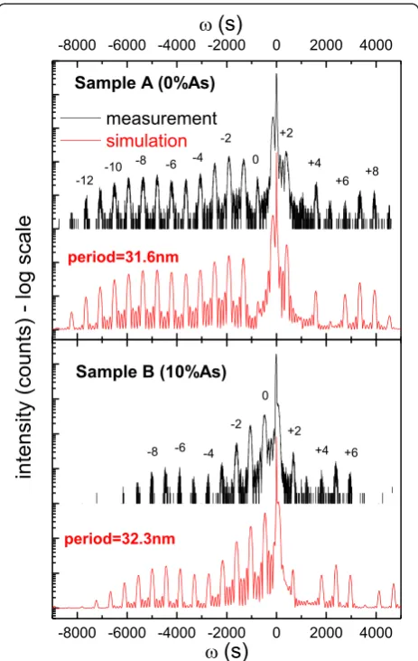
the simulations (shown in red color) allowed for the deter-mination of layer thicknesses which agreed very well with the nominal ones. The comparison between simulated and measured curves gives the fundamental structure period (a sum of QW layer thicknesses and the separating barrier) of 31.6 nm for sample A and 32.3 nm for sample B confirming that the real QW parameters are indeed close to the nominal ones. The small discrepancies are ra-ther within the accuracy of the fit.
To probe the structural quality of the layers, cross-sectional STEM measurements have been performed in the high-angle annular dark field (HAADF) mode. Speci-mens from the samples were prepared for STEM using conventional mechanical polishing (down to a thickness of approximately 20 μm) and argon ion milling utilizing the precision ion polishing system of Gatan and follow-ing the <110> crystallographic direction. This is obtained thanks to the size of the ion beam (approximately 1 mm
large) and utilization of the natural nonuniformity of the etching. The process is stopped when a hole appears at the center of the thin foil. Sample thickness is increasing gradually, as one moves away from the center. Parts of the sample that are thin enough to be transparent to electrons are located around the hole. Before the ion-thinning process, the thin sample was glued onto a cop-per ring. The final specimen thickness was between 25 and 50 nm. Prior to STEM imaging, the specimens were cleaned using an argon plasma cleaner. HAADF STEM and energy-dispersive X-ray spectroscopy (EDX) were performed in an aberration-corrected JEOL 2200FS microscope, operating at 200 kV with a probe current of 150 pA and the full width at the half maximum (FWHM) of the probe being 0.12 nm. The convergence half-angle of the probe was 30 mrad, and the detection inner and outer half-angles for the STEM images were 100 and 170 mrad, respectively. In order to probe the composition across the layers, the EDX technique has been used, based on the intensity ratio of the respective X-ray spectral lines. The acquisition time for each EDX spectrum was 60 s, during which no drift in the position of the electron beam was observed. Further experimental details can be found elsewhere [18, 19].
In order to measure photoluminescence (PL) and photoreflectance (PR) spectra [20–22] in that spectral range, we utilized a setup based on a Fourier transform and vacuum spectrometer Bruker Vertex 80v operated in step-scan mode and equipped with an external chamber for experiments employing an additional mechanically modulated laser beam. In this case, a liquid-nitrogen-cooled InSb photodiode was used as a detector. In both measurement configurations, the pump beam was pro-vided by the 660-nm line of a semiconductor laser diode, modulated with a frequency of 275 Hz. Phase-sensitive de-tection of the optical response was performed using a lock-in amplifier.
Results and Discussion
It has been revealed previously [14, 15] that incorpor-ation of arsenic into the GaInSb layer of the W-design II QW system provides additional possibilities in terms of band alignment and strain tailoring and allows for the enhancement of oscillator strength of the active type II transition. All those can generally be considered as bene-ficial from a band structure engineering point of view and also help to improve the performance of interband cascade lasers. On the other hand, however, the addition of arsenic seems to have generated interface localized states, which can trap the carriers decreasing the radia-tive efficiency of emission from this kind of quantum wells [15]. Hereby, we report on the observation of an-other side effect, related to the compositional changes in the hole-confining layer, affecting the entire type II
Fig. 1HR-XRD spectra for the type II QWs with various As contents:
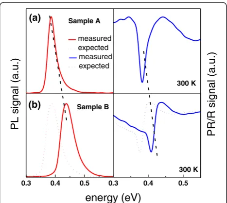
[image:3.595.58.290.88.454.2]system, which can be crucial for properly predicting the electronic structure, as well as for device fabrication with the demanded emission wavelength. In Fig. 2, room temperature (300 K)-normalized PL and PR spectra measured for the investigated samples are presented. The single peaks in the PL spectra are related to the ground state type II transition in the QWs. The same transition is detected in the PR spectra. These lines are related to the 1e–1h transition, where 1e means the first electron level confined in the InAs layers and 1h the first hole level confined in the GaIn(As)Sb layer. The energy of the transition for sample B is shifted towards blue (shown by black dashed lines) after incorporation of As into the valence band well layer. The dotted lines in Fig. 2 represent the theoretically predicted position of these spectra, i.e., for an ideally rectangular QW profile [23–26], which results from several composition-related effects. The primary influence on the ground state tran-sition energy shift is attributed to the As-induced band gap change [27]. Important contributions come from strain modification in the GaIn(As)Sb layer and changes of the confinement potential; that is, in the type II sys-tem with two InAs layers, the change of the GaInAsSb energy gap entails also a change of the barrier height and the resulting coupling. A reasonable agreement between the theory and experiment has only been dem-onstrated for sample A, with the ternary GaInSb layer. However, the energy shift for sample B in the experi-ment is opposite to that predicted by the model. The ex-perimental behavior may suggest that incorporation of
arsenic into the GaInSb layer could change the profile of the QW in such a way as to result in electronic structure modification, eventually causing a blueshift instead of a redshift. The measured energy blueshift cannot be ex-plained by QW layer width changes because, as it was previously shown above, the obtained periods provided by XRD spectra are almost the same for both samples and very close to the nominal values. In our previous article [15], we have already demonstrated that arsenic can have a strong impact on the InAs/GaInAsSb inter-faces. Therefore here, for better understanding of these effects, we have analyzed the atomic resolution HAADF-STEM images of the investigated samples in the cross-sectional plane perpendicular to the interfaces. This image is presented in Fig. 3. The interfaces are very sharp for the ternary layer structure (sample A) and already a bit smeared out for the As-containing structure (sample B) (the mentioned interfaces are shown by dashed black lines). Although the interfaces between the InAs and GaI-n(As)Sb layers can barely be seen for both the cases, due to the natural low image contrast for these materials, these STEM images already suggest an enhanced intermixing after the addition of arsenic.
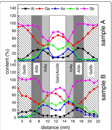
In order to interpret the results more quantitatively, we have also performed EDX analysis of the samples. The blue trace over the sample’s STEM cross-sectional plane image (example shown for sample B—right side of Fig. 3) corresponds to points used for EDX analysis. A single spot in this analysis is about 1.5 nm wide. The re-sults are presented as full symbols in Fig. 4. Despite the convolution with the probe size, and hence quite a lim-ited resolution of the composition determination when compared to the thicknesses of the layers, we can ob-serve a clear variation of the composition inside the structure. Various elements are represented by different colors in Fig. 4, whereas the colors of the background indicate the nominal layer thicknesses. Although the resolution of the composition contrast is low, comparing
PR/R si
g
nal (a.u.)
300 K
PL signal (a.u.)
(a) Sample A
measured expected measured expected
0.3 0.4 0.5
(b)
300 K
Sample B
0.3 0.4 0.5
energy (eV)
Fig. 2Room temperature photoluminescence (red lines—left part)
and photoreflectance (blue lines—right part) spectra of ground state type II“W”-shaped quantum well transitions measured for sample A (a) and sample B (b).Dotted linesshow the expected spectra at the calculated nominal transition energy
LG1
GaInSb
GaInAsSb
Fig. 3HAADF-STEM images for samples A and B.Blue circlesrepresent
[image:4.595.57.291.465.674.2] [image:4.595.304.538.558.675.2]the results for samples A and B allows us to see that the smoothening of the interfaces for the latter, i.e., en-hancement of the intermixing of the atoms and finally creation of the less clearly defined interfaces between layers, can be observed. The atoms’ intermixing is the reason for the electronic structure modification, leading to the confined level shifts and, consequently, a blueshift of the ground state transition energy for the sample with a thin GaInAsSb layer (used for hole confinement) with re-spect to the reference structure containing a GaInSb layer. Considering EDX profiles showing interface changes for sample B, we propose the following changes of the QW potential shape for the investigated samples. The composition profile of the sample with interface intermix-ing at the boundaries of the quaternary layer has been modeled by the Gauss error function [28, 29]—typically used to describe interdiffused interfaces. Figure 5 shows changes of the QW shape for three different values of the effective diffusion lengthsLd(which is not exactly known
for our structures). Ldis tuned in a way to get the best
agreement of the energy level spacing and outgoing op-tical transitions with those observed in the experiment as seen in Fig. 2. The concentration profile of groups III and V in the QW is given by:
w zð Þ ¼w2−w2−w1
2 erf
Lþ2z 4Ld
þerf L−2z 4Ld
wherew1and w2are the initial concentrations of atoms in the well and in the barrier, respectively, L is the as-grown nominal width of the QW, z is the quantization direction along the growth axis (QW centered at z= 0), and“erf”denotes the error function. For sample A, small modifications of the interfaces (e.g., Ld= 1.5 nm) do not change the optical transition energies significantly and the agreement with the experiment remains good—see Table1(i.e., the correction due to the inclusion of inter-mixing is of the order of a few millielectronvolts). For sample B, a much stronger modification had to be used (Ld= 5 nm) to obtain agreement with the experimental value (see Table1).
This confirms that the stronger intermixing in the As-containing structures can indeed cause a blueshift of the optical transition instead of the redshift which would be ex-pected for rectangular—or less interdiffused—structures. The intermixing might be due to the finite time (roughly 2 s) that the As valve takes to change its position, and hence the flux, after the first InAs layer and before the second InAs layer. This causes some gradient in As concentration, which can be understood as intermixing.
0 20 40 60 80 100 120 140
4 6 8 10 12 14 16 18 20 22 0
20 40 60 80 100 120 140
sample B
InAs InAs
content (%)
Al Ga As In Sb
sample A
GaIn(As)Sb
Ga
Sb
Ga
Sb
AlSb
distance (nm)
AlSb
Fig. 4EDX profiles of the investigated samples (solid symbols).
Various colorsrepresent different elements in subsequent layers. In the background,colored areasdemonstrate the nominal thickness of each layer
-0.5 0.0 0.5 1.0 1.5 2.0
-0.5 0.0 0.5 1.0 1.5 2.0
240 280 320 360
-0.5 0.0 0.5 1.0 1.5 2.0
L
d
= 0.0
(a)
395meV
(b)
energy (eV)
L
d
= 1.5
388meV
(c)
z (nm)
L
d
= 5.0
415meV
Fig. 5QW profiles for the nominal parameters of sample A (a),
[image:5.595.57.292.87.359.2] [image:5.595.307.540.87.383.2]Any attempts of using shutter sequencing combined with growth interruptions within the W-QW have led to sam-ples that did not exhibit any PL signal. Summarizing, we have shown that interface quality has a significant impact on the energy structure in our type II quantum wells, similarly as to what was previously shown for other low dimensional systems like, e.g., type I quantum wells [28], superlattices [30], and quantum dots [31].
Conclusions
In conclusion, type II “W”-shaped GaSb/AlSb/InAs/ GaIn(As)Sb/InAs/AlSb/GaSb QWs have been investi-gated. Optical spectroscopy (photoluminescence and photoreflectance) combined with band structure calcula-tions made in the eight-band k·p formalism has been used to investigate the fundamental optical transition. These have been supported by HAADF-STEM images and EDX analysis in association with the numerical modeling of interface intermixing to show the changes in QW element compositions and prove an apparent ar-senic effect on the structural and optical properties of type II “W”-shaped QW with quaternary GaInAsSb layers. We have shown that incorporation of arsenic into the GaInSb hole-confining layer does not only change the composition-driven energy gap and strain but also has a strong impact on the InAs/GaInAsSb interface. This affects the electronic structure of the quantum well to such an extent that it leads to an increasing blueshift of ground state type II transition with the increase of arsenic content in this layer. These results indicate that this effect should be taken into account when considering such QWs for the design of active regions of improved per-formance interband cascade lasers and that additional work on the technological side is necessary to minimize interface diffusion when GaInAsSb layers are utilized.
Abbreviations
EDX:Energy-dispersive X-ray spectroscopy; HR-XRD: High-resolution X-ray dif-fraction; PL: Photoluminescence; PR: Photoreflectance; QWs: Quantum wells; STEM: Scanning transmission electron microscopy.
Competing interests
The authors declare that they have no competing interests.
Authors’contributions
MM wrote this article and made substantial contributions to the acquisition of spectroscopic data. GS contributed to the analysis of data. KR performed the calculations. MD contributed to the acquisition of spectra. RW performed the MBE growth. GP made EDX spectroscopy and provided the STEM images. JM, SH, and MK have been involved in drafting the manuscript. All authors read and approved the final manuscript.
Acknowledgements
The work has been supported by Project Widelase (no. 318798) of the Seventh Framework Programme of the European Commission.
Author details
1
Laboratory for Optical Spectroscopy of Nanostructures, Department of Experimental Physics, Faculty of Fundamental Problems of Technology, Wrocław University of Technology, Wybrzeże Wyspiańskiego 27, Wrocław, Poland.2Technische Physik and Wilhelm-Conrad-Röntgen-Research Center for Complex Material Systems, University of Würzburg, Am Hubland, 97074 Würzburg, Germany.3Laboratoire de Photonique et de Nanostructures, CNRS, Université Paris-Saclay, Route de Nozay, 91460 Marcoussis, France.4School of Physics and Astronomy, University of St. Andrews, North Haugh, KY16 9SS St. Andrews, UK.
Received: 18 August 2015 Accepted: 1 December 2015
References
1. Kluczynski P, Jahjah M, Nähle L, Axner O, Belahsene S, Fischer M, et al. Detection of acetylene impurities in ethylene and polyethylene manufacturing processes using tunable diode laser spectroscopy in the 3-μm range. Appl Phys B. 105:2011. doi: 10.1007/s00340-011-4645-6 2. Vizbaras K, and Amann M-C. Room-temperature 3.73μm GaSb-based
type-I quantum-well lasers with quinternary barriers. Semicond Sci Technol 27:2012. doi:10.1088/0268-1242/27/3/032001
3. Sęk G, Motyka M, Ryczko K, Janiak F, Misiewicz J, Belahsene S, et al. Band offsets and photoluminescence thermal quenching in mid-infrared emitting GaInAsSb quantum wells with quinary AlGaInAsSb barriers. Jpn J Appl Phys 49:2010. doi:10.1143/JJAP.49.031202
4. Mawst LJ, Kirch JD, Chang CC, Kim T, Garrod T, Botez D, et al. InGaAs/AlInAs strain-compensated superlattices grown on metamorphic buffer layers for low-strain, 3.6μm-emitting quantum-cascade-laser active regions. J Cryst Growth 370:2013. doi:10.1016/j.jcrysgro.2012.06.053
5. Kruczek T, Fedorova KA, Sokolovskii GS, Teissier R, Baranov AN, Rafailov EU. InAs/AlSb widely tunable external cavity quantum cascade laser around 3.2μm. Appl Phys Lett 102:2013. doi:10.1063/1.4774088
6. Yang RQ. Infrared laser based on intersubband transitions in quantum wells. Superlattices Microstruct 17: 1995. doi:10.1006/spmi.1995.1017
7. Meyer JR, Hoffman CA, Bartoli FJ, Ram-Mohan LR. Type-II quantum-well lasers for the mid-wavelength infrared. Appl Phys Lett 67:1995. doi:10.1063/1.115216 8. Motyka M, Sęk G, Ryczko K, Misiewicz J, Lehnhardt T, Höfling S, et al.
Optical properties of GaSb-based type II quantum wells as the active region of midinfrared interband cascade lasers for gas sensing applications. Appl Phys Lett 94:2009. doi:10.1063/1.3157910
9. Motyka M, Ryczko K, Sęk G, Janiak F, Misiewicz J, Bauer a., et al. Type II quantum wells on GaSb substrate designed for laser-based gas sensing applications in a broad range of mid infrared. Opt Mater (Amst) 34:2012. doi:10.1016/j.optmat.2012.01.012
10. Vurgaftman I, Bewley WW, Canedy CL, Kim CS, Kim M, Merritt CD, et al. Rebalancing of internally generated carriers for mid-infrared interband cascade lasers with very low power consumption. Nat Commun 2:2011. doi:10.1038/ncomms1595
11. Bauer A, Hofling S, Worschech L. German Patent No. DE 10 2011 103 143 A1. 2012.
12. Sęk G, Janiak F, Motyka M, Ryczko K, Misiewicz J, Bauer a., et al. Carrier loss mechanisms in type II quantum wells for the active region of GaSb-based mid-infrared interband cascade lasers. Opt Mater (Amst) 33:2011. doi:10.1016/j.optmat.2011.06.019
[image:6.595.56.541.112.153.2]13. Nilsen TA, Breivik M, Selvig E, Fimland BO. Critical thickness of MBE-grown Ga1-xInxSb (x<0.2) on GaSb. J Cryst Growth 311:2009. doi:10.1016/j.jcrysgro.2008.11.083
Table 1Experimental and calculated fundamental type II transition energies for two samples with As content in W-design GaSb/ AlSb/InAs/Ga0.665In0.335AsxSb1−x/InAs/AlSb/GaSb QWs equal to 0 and 10 %, respectively
Sample As content (%) Experiment (eV) Calculated—nominal (eV) Calculated—intermixing (eV)
A 0 0.386 0.395 0.388
14. Janiak F, Sęk G, Motyka M, Ryczko K, Misiewicz J, Bauer A, et al. Increasing the optical transition oscillator strength in GaSb-based type II quantum wells. Appl Phys Lett 100:2012. doi:10.1063/1.4726423
15. Janiak F, Motyka M, Sęk G, Dyksik M, Ryczko K, Misiewicz J, et al. Effect of arsenic on the optical properties of GaSb-based type II quantum wells with quaternary GaInAsSb layers. J Appl Phys 114:2013. doi:10.1063/1.4846756 16. Ryczko K, Sęk G, Misiewicz J. Eight-band k p modeling of InAs/InGaAsSb
type-II W-design quantum well structures for interband cascade lasers emitting in a broad range of mid infrared eight-band k p modeling of InAs/InGaAsSb type-II W-design quantum well structures for interband cascade lasers emitting in a broad range of mid infrared. J Appl Phys 114:2013. doi:10.1063/1.4843076
17. Ryczko K, Liszka T. Tailoring the effect of electric field in type II W-design InAs/GaInSb quantum well structures for emission up to 12μm. Superlattices Microstruct 78:2015. doi:10.1016/j.spmi.2014.11.032
18. Pantzas K, Patriarche G, Talneau A, Youssef J Ben. Bonding mechanism of a yttrium iron garnet film on Si without the use of an intermediate layer. Appl Phys Lett 105:2014. doi:10.1063/1.4896978
19. Priante G, Patriarche G, Oehler F, Glas F, Harmand J-C. Abrupt GaP/GaAs interfaces in self-catalyzed nanowires. Nano Lett 15:2015. doi:10.1021/acs.nanolett.5b02224
20. Hosea TJC, Merrick M, and Murdin BN. A new Fourier transform photo-modulation spectroscopic technique for narrow band-gap materials in the mid- to far-infra-red. Phys Status Solidi 202:2005. doi:10.1002/pssa.200460908
21. Shao J, Lu W, Yue F, Lü X, Huang W, Li Z, et al. Photoreflectance spectroscopy with a step-scan Fourier-transform infrared spectrometer: technique and applications. Rev Sci Instrum 78:2007. doi:10.1063/1.2432269 22. Motyka M, Sęk G, Janiak F, Misiewicz J, Kłos K, and Piotrowski J.
Fourier-transformed photoreflectance and fast differential reflectance of HgCdTe layers. The issues of spectral resolution and Fabry–Perot oscillations. Meas Sci Technol 22:2011. doi:10.1088/0957-0233/22/12/125601
23. Meney AT, Gonul B, O’Reilly EP. Evaluation of various approximations used in the envelope-function method. Phys Rev B 50:1994. doi:10.1103/ PhysRevB.50.10893
24. Ridene S, Boujdaria K, Bouchriha H, Fishman G. Infrared absorption in Si/Si(1−x)Ge(x)/Si quantum wells. Phys Rev B 64:2001. doi:10.1103/ PhysRevB.64.085329
25. Ryczko K, S k G, Sitarek P, Mika A, Misiewicz J, Langer F, et al. Verification of band offsets and electron effective masses in GaAsN/GaAs quantum wells: spectroscopic experiment versus 10-band k·p modeling. J Appl Phys 113:2013. doi:10.1063/1.4810920
26. Muñoz M, Pollak FH, Zakia MB, Patel NB, Herrera-Pérez JL. Temperature dependence of the energy and broadening parameter of the fundamental band gap of GaSb and Ga1-xInxAsySb1-y/GaSb (0.07≤x≤0.22, 0.05≤y≤0.19) quaternary alloys using infrared photoreflectance. Phys Rev B - Condens Matter Mater Phys 62:2000. doi:10.1103/PhysRevB.62.16600
27. Munoz M, Wei K, Pollak FH, Freeouf JL, Wang C a, Charache GW. Optical constants of Ga1-xInxAsySb1-y lattice matched to GaSb (001): experiment and modeling. J Appl Phys 87:2000. doi:10.1063/1.372092
28. Ryczko K, Sęk G, Motyka M, Janiak F, Kubisa M, Misiewicz J, et al. Effect of annealing-induced interdiffusion on the electronic structure of mid infrared emitting GaInAsSb/AlGaInAsSb quantum wells. Jpn J Appl Phys 50:2011. doi:10.1143/JJAP.50.031202
29. Chen H, McKay H a., Feenstra RM, Aers GC, Poole PJ, Williams RL, et al. InGaAs/InP quantum well intermixing studied by cross-sectional scanning tunneling microscopy. J Appl Phys 89:2001. doi:10.1063/1.1361237 30. Jasik A., Sankowska I, Pierścińska D, Regiński K, Pierściński K, Kubacka-Traczyk
J. Blueshift of bandgap energy and reduction of non-radiative defect density due to precise control of InAs-on-GaSb interface in type-II InAs/ GaSb superlattice. J Appl Phys 110:2011. doi:10.1063/1.3671024 31. Dai L, Bremner SP, Tan S, Wang S, Zhang G, Liu Z. Suppression of
dislocations by Sb spray in the vicinity of InAs/GaAs quantum dots. Nanoscale Res Lett 9:2014. doi:10.1186/1556-276X-9-278
Submit your manuscript to a
journal and benefi t from:
7Convenient online submission 7Rigorous peer review
7Immediate publication on acceptance 7Open access: articles freely available online 7High visibility within the fi eld
7Retaining the copyright to your article