Highly reproducible perovskite solar cells via controlling
the morphologies of the perovskite thin films by the
solution-processed two-step method
RAHAQ, Yaqub, MOUSSA, Magdi, WANG, Heming and HASSAN, Aseel <http://orcid.org/0000-0002-7891-8087>
Available from Sheffield Hallam University Research Archive (SHURA) at:
http://shura.shu.ac.uk/22137/
This document is the author deposited version. You are advised to consult the publisher's version if you wish to cite from it.
Published version
RAHAQ, Yaqub, MOUSSA, Magdi, WANG, Heming and HASSAN, Aseel (2018). Highly reproducible perovskite solar cells via controlling the morphologies of the perovskite thin films by the solution-processed two-step method. Journal of Materials Science: Materials in Electronics, 1-11.
Copyright and re-use policy
See http://shura.shu.ac.uk/information.html
Highly reproducible perovskite solar cells via controlling the morphologies
of the perovskite thin films by the solution-processed two-step method
Yaqub Rahaq, Magdi Moussa, Abubaker Mohammad, Heming Wang, Aseel Hassan*
Materials & Engineering Research Institute, Sheffield Hallam University, City Campus, Howard Street, Sheffield, S1 1WB
*Corresponding author: aseel50.hassan@gmail.com
Abstract
Organic-inorganic halide perovskites are one of the most attractive materials for the next
generation solar cells. The PCE has rapidly increased to more than 22% using different
configurations and techniques and further developments are predicted. However, perovskite
solar cells suffer from fabrication reproducibility mainly due to difficulty in controlling the
morphology of the perovskite films themselves. In this paper we present a low temperature
solution-processed two-step deposition method to fabricate CH3NH3PbI3 perovskites. This
method offers a simple route with great potential in fabricating reproducible perovskite solar
cells. In the present work, we demonstrate that the morphology of the perovskite thin films is
highly determined by the concentration of Methylammonium iodide (MAI) as well as the
reaction time between MAI and PbI2. High-performance solar cells have been reproducibly
achieved with a highest PCE of 15.01% for PCBM-based planar heterojunction solar cells.
Key words: Halide perovskite; Solar cell; Films’ morphology; Solution-processing,
1. Introduction
Organometallic halide perovskites have received significant interests in the last few years due
to their superior optical and electrical properties. They demonstrated highly efficient
capability of converting light into electricity with low-cost precursors and inexpensive
solution-processed methods in fabricating the solar cells [1-7]. Power conversion efficiency
(PCE) of perovskite solar cells has considerably soared from 3.8% in 2009 [8] to the certified
efficiency of 22.7% in 2018 [9]. Studied perovskites solar cells were based on two types of
typical device architectures, one type is based on TiO2 [10-15] films and the other is based on
phenyl-C61-butyric acid methyl ester (PCBM) planar heterojunction (PHJ) [16-20]. In order
to achieve solar cells with high PCE, controlling the morphology of the perovskite thin films
is one of the major challenges. In the published literature, perovskite films were produced by
various methods, which include vacuum thermal deposition and solution-processed
deposition by either one-step or two-step methods. Using the latter method, high-quality
perovskite films were obtained utilising both approaches, with solar cells achieving high
PCE. On the other hand, the major obstacle to the thermal evaporation method is ascribed to
the high-cost of vacuum systems as well as its complicated processes. Furthermore, in order
to control the morphology of the perovskite thin films in the one-step solution-processing
method, two main routes were utilised; i) by adding additives into the precursor solution of
the perovskites, and ii) by employing the so-called solvent engineering technology [21].
Nevertheless, it was found that uniform morphologies are difficult to be re-produced in the
one-step method owing to their uncontrollable crystallisation rate during the fabrication
process [22]. Therefore, the two-step method has been widely adopted as an efficient
technique to control the morphology of the perovskite layer for both TiO2-based and the
controlling the concentration in one of the precursors, and therefore controlling their reaction
and crystallisation rates. For the TiO2-based perovskite solar cells, different techniques were
applied to control the morphologies including vapor-assisted solution-processing [23], halide
sources mixing method [24], low-temperature gas-solid crystallisation processes [25],
solution chemistry engineering [26], anti-solvent vapour-assisted crystallisation processes
[27], and two-step ultrasonic spray deposition method [28]. Those methods however are
complicated and may be expensive in some cases, although high-performance solar cells
were obtained utilising one or another of the above highlighted methods. Furthermore, the
TiO2 layer has to be sintered at temperatures around 500°C [2], adding further difficulty to
the processing of reliable TiO2-based solar cells. Alternatively, the two-step fabrication
method for the PCBM-based perovskite solar cells demonstrates a low-temperature
processing route with favourable benefits as well as increased control of the perovskite films’
morphologies. Different strategies have been used to control the crystallisation and to
improve the morphologies of perovskite thin films in the PCBM-based perovskite solar cells.
Shen et.al have employed the two-step annealing process to fabricate CH3NH3PbI3 (assisted
by doping with PbCl2) perovskites thin films [29]. They found that thermal annealing has
improved the surface coverage as well as the crystallisation of the perovskite films. PCE of
9.1% was achieved for solar cells based on this fabrication approach [29]. Haung et al
claimed that the application of solvent annealing in the fabrication of perovskite films is an
efficient technique to enhance the crystallinity of the perovskites, achieving 1 μm grain size
of perovskites. The DMF was thought to promote grain growth due to the high solubility of
both PbI2 and MAI in DMF where the latter provide wet environment for the precursor ions
and molecules to diffuse longer distance than in the case of all-solid annealing. Solar cells
produced using such perovskite films have achieved PCE of 15.6% [30]. Chen and
[31]. PbCl2 thin film was deposited by thermal evaporation, followed by dipping the film into
a solution of CH3NH3I/IPA for several times to form a uniform perovskite layer [31]. Both
solvent annealing and thermal annealing were shown to play a key role in controlling the
crystal growth of the perovskites towards improvement of its morphology in the two-step
method. However, various other factors can significantly affect the solvent annealing process,
such as type and vapour pressure of solvents, process surrounding, and thermal annealing
conditions (annealing temperature, duration and ramping level) [32]. Furthermore, reaction
time between the pre-coated metal halide and MAI layer after being dipped into the solution
of MAI requires an accurate control [23].
In this paper, we present a simple route to control the morphology of our perovskite films by
the two-step deposition method used for the fabrication of PCBM-based PHJ solar cells.
Through wide investigation of alternating the MAI concentration and its reaction time with
the pre-deposited PbI2 film, high-performance perovskite films were reproducibly obtained,
resulting in perovskite solar cell structure with PCE of 15%. This technique has led to
controlling the growth of perovskite crystals resulting in more compact film structure without
pin holes and therefore leading to enhanced PCE of the perovskite film-based solar cell.
Morphology and crystallinity of our perovskite films were extensively studied using SEM
and XRD measurements.
2. Experimental
2.1 Preparation of materials
MAI was synthesised in ambient atmosphere at room temperature via the chemical reaction
of 27 ml methylamine solution (CH3NH2, 40 wt% in methanol, TCI) with 30 ml of hydriodic
acid (HI 57 wt.% in water, Aldrich) in a round-bottomed flask kept at 0 °C in an ice bath for 2
added drop-wise during stirring. White precipitate of MAI was collected after the mixture in
the solution was transformed into a rotary evaporator and heated at 50°C for 1 h. The white
precipitate was washed three times with diethyl ether and finally dried in vacuum for 24 h.
PbI2 solution was prepared by dissolving 1 mole PbI2 in 1 ml DMF solvent and stirred at
70 °C. 20 μl of DIO was then added into the solution to promote the dissolution of PbI2. The
PbI2 solution became clear after continuous overnight stirring at 70 oC. Thereafter, 0.5, 0.8,
1.0, 1.2 wt% MAI solution were separately produced by adding different amounts of MAI in
2-propanol and stirred for 1 h at 70°C. The PCBM solution was prepared by dissolving 30 mg
of PCBM in 1 ml of chlorobenzene. 2 mg of bathocuproine (BCP) plus 20 μl acetic acid was
dissolved in 1 ml of methanol to form the BCP solution.
2.2 Fabrication of solar cells
In the current study perovskite solar cells architecture comprises thin films of
ITO/PEDOT:PSS/CH3NH3PbI3/PCBM/BCP/Au, respectively; a flow chart illustrating the
fabrication process is shown in Figure 1. ITO-coated glass substrates (ITO thickness is 100
nm) with sizes of ~ 20 x 25 mm were cleaned with soap and water followed by washing in
deionised (DI) water. The substrates were blown dry in N2 gas before they were separately
cleaned ultrasonically in acetone and 2-propanol and finally blown dry again by N2. The
cleaned ITO substrates were spin-coated by PEDOT:PSS solution at spin speed of 3000 rpm
followed by heating at 140 °C for 10 min. Thin films of PbI2 were deposited on top of the
PEDOT:PSS film by spin-coating at 5000 rpm using the high-purity supersaturated hot
solution and then annealed at 70 °C for 8 min on a hot plate. MAI solution with different
concentrations was added by drop casting on top of the PbI2 thin film and left to react
chemically with PbI2 for various periods of time. The reactants were finally spin-casted at a
rotation speed of 4000 rpm, and the obtained films were heated treated at 100 oC for 2 h.
top of the formed perovskite thin film, followed by heat treatment at 100 °C for 30 min.
Electron transport layers of BCP of about 10 nm in thickness were spin-coated on top of the
BCPM films followed by the deposition of Au films of about 100 nm as the top electrode
using vacuum sputtering method.
2.3 Characterisation of solar cells
Current density as a function of applied voltage (J-V) of the PV devices fabricated in section
2.2 were measured under simulated AM 1.5G irradiation (100 mW/cm2) using keithley 2401
source meter; the measurements were carried out under ambient environment. A Schott KG5
colour-filtered Si diode (Hamamatsu S1133) was utilised to calibrate the light intensity of the
solar light simulator before J-V measurement were carried out. An aperture of aluminium
mask was applied on the PV devices to obtain an active area of 0.04 cm² and to prevent any
contribution from externally fallen light on the devices. X-ray diffraction (XRD)
measurements of the perovskite layers were performed using Philips X’PERT MPD with
operational parameters of 40 kV and 40 mA. Optical properties of the films were analysed
using Varian 50 Scan UV–Vis Spectrophotometer. Scanning electron microscopy (SEM) was
used to investigate morphology of the perovskite films using FEI-nova nanosem 200 SEM..
3. Results and discussion
3.1 MAI concentration effects on the perovskite crystal growth
Different concentrations of MAI in the range 0.5-1.2 wt% were separately utilised to apply
onto the pre-coated PbI2 thin films and allowing different reaction times (20 and 60 sec),
followed by thermal annealing of the obtained perovskite films at 100°C for 2 hour.
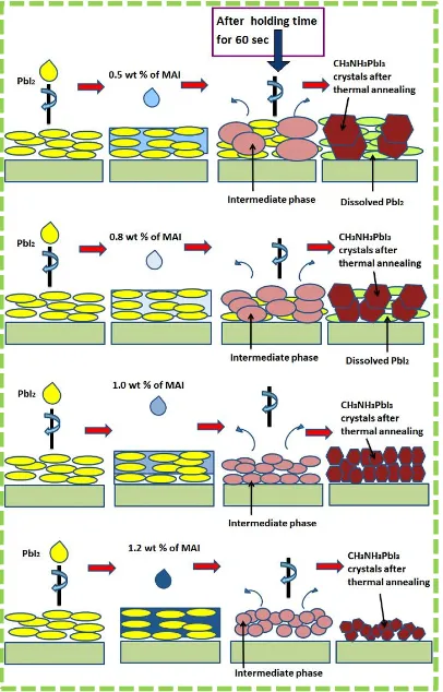
A processing model to describe the formation of the perovskite thin film with different
Figure 2. When the MAI solution reached to the pre-coated PbI2 crystals, nucleation of an
intermediate phase of perovskites only happened at those areas where the MAI concentration
must be greater than a threshold concentration (Ck); lower concentrations of MAI than Ck is
not expected to result in such crystal growth. A specific reaction time between MAI and PbI2
allows the growth of an intermediate phase of perovskite. This intermediate phase is then
transformed into full perovskite phase after the film is thermally annealed at 100oC. When the
lower concentration of 0.5 or 0.8 wt% of MAI solution were applied onto the pre-formed PbI2
film (as shown in Figure 2) only a small perturbation in the MAI concentration has led to
some areas with locally high concentration of MAI, which resulted in the formation of a
sporadically distributed intermediate phase of CH3NH3PbI3. Only when the concentration of
MAI increased to 1.0 wt%, the distributed amount of MAI on the whole surface area of the
PbI2 film was maintained at a concentration above Ck, and thus a gradually controlled crystal
growth happened. Thin films with a uniform intermediate perovskite phase were formed after
the reaction was maintained for about one minute. Longer growth (reaction) time and higher
concentration of MAI will lead to the lift-off of the intermediate perovskite phase from the
substrate, which will then lead to reduction in the thickness of the final perovskite film by the
following spin-coating process.
Scanning electron microscopy (SEM) was used to study the morphology of the perovskite
films and the results are shown in Figure 3. When the lowest concentration of 0.5 wt% MAI
was added onto the pre-coated PbI2 film, the size of the perovskite crystals increased from ~
0.7 µm for the 20 sec reaction time to ~ 1.0 µm for the 60 sec reaction time, as seen in Figure
3a and 3b. When comparing Figure 3a with Figure 3b, the slightly dissolved PbI2 film was
observed except the sporadically distributed perovskite crystals, which did not cover the
whole surface. In other words, most of the PbI2 crystals were only slightly dissolved by the
crystallisation of the perovskites. Further increase in the reaction time between MAI and PbI2
did not make any contribution to the enhancement of the nucleation density on the surface of
the PbI2 film. Interestingly, with the increase of the MAI concentration to 0.8 wt%, we
noticed that crystallisation occurred with an increased surface coverage on the PbI2 thin film
as indicated in Figure 3c and 3d. However, the size of the perovskite crystals decreased to ~
0.4 µm regardless of how long the reaction time was. With a further increase of the MAI
concentration to 1.0 wt%, the coverage of the perovskite surface reached full coverage of the
original PbI2 surface, meaning that all PbI2 crystals have reacted with MAI to form
perovskites as shown in Figure 3e and 3f. Again, we observed that the size of perovskites
continued to decrease to about 0.2 µm.
Nevertheless, when the concentration of the MAI solution further increased to 1.2 wt %, pore
defects among the smaller nano-sized perovskite crystals were revealed in Figure 3g and 3h.
As shown in Figure 3, the size of the perovskite crystals in the film did not change with
extending reaction time from 20 sec to 60 sec when using high concentrations of 0.8, 1 and
1.2 wt % of MAI solutions. These results confirm that the size of crystals in the perovskite
film was determined in the initial reaction stage when the MAI solution came into contact
with the pre-coated PbI2.
SEM was also used to further study the morphology of the cross section of the perovskite
films and the results are shown in Figure 4. Figure 4a shows a cross section SEM image of
the perovskite film fabricated by the 0.8 wt% MAI solution, where the corresponding
thickness of the perovskite film was ~ 400 nm. The image shows that the nano-sized
polycrystals of CH3NH3PbI3 did not connect together as was also shown in Figure 3c and 3d,
where considerable residual PbI2 phases have existed in the film. As demonstrated in Figure
3e and 3f, interconnected CH3NH3PbI3 crystals without any residual PbI2 phases were only
the perovskite film was ~ 200 nm as demonstrated in Figure 4b. A further increase in the
MAI solution concentration to 1.2 wt% has led to the formation of pore defects among the
smaller nano-sized perovskite crystals as revealed in Figure 3g and 3h. The thickness of the
perovskite film has exhibited a significant decrease to ~120 nm as demonstrated by the cross
section image in Figure 4c.
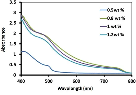
3.2 Effect of MAI concentration on light absorption and crystal structure of perovskite films
Light absorption by the formed perovskite films was examined to study the impact of the
MAI concentrations on the optical properties of the perovskite films. All perovskite films
with different MAI concentrations show absorption onset at ~ 780 nm as shown in Figure 5,
which could conform to a band gap value of ~1.52 eV for the perovskites. The perovskite
film produced by the low concentration of 0.8 wt% MAI exhibited the highest thickness as
shown in Figure 4a, and thus the highest light absorption. On the other hand, the perovskite
film obtained by the highest MAI concentration of 1.2 wt% resulted in the lowest thickness
which is associated with a significant decrease in the absorption intensity as demonstrated in
Figure 5. The perovskite thin film produced from the 1.0 wt% MAI solution showed an
excellent light absorption between the perovskite films obtained by 0.8 wt% and 1.2 wt%
MAI solutions.
X-ray diffraction measurements (XRD) were used to characterise the crystalline structure of
the perovskites films produced with different MAI concentrations and the results are
presented in Figure 6. All perovskite films were prepared under the same condition on glass
slides with exactly the same size. Diffraction peaks that belong to CH3NH3PbI3 polycrystals
are indicated by “” while the main peaks assigned to the residual PbI2 phase are illustrated by “●”. The XRD pattern of the film produced from the lowest MAI concentration (0.5 wt%)
42.6° and 52°. Most peaks belong to the perovskite structure except the peaks at 8.2° and
12.8° are due to the residual PbI2 phase. According to Qiu and co-workers, the measured
peaks at 2Ɵ of 14.2°, 20.09°, 23.8°, 28.4°, 31.9°, 40.7° and 42.6° may correspond to the
(110), (112), (211), (220), (310), (224) and (314) crystal faces of the tetragonal perovskite
[33]. The high intensity of the two peaks at 2Ɵ of 8.2° and 12.8° indicates the considerable
presence of residual PbI2 phases in the sample. Increasing the MAI concentration to 0.8 wt%
led to more perovskite phases in the film as shown in Figure 6, where the two peaks assigned
to the residual PbI2 phase have reduced significantly. When the MAI concentration reached
1.0 wt%, only peaks assigned to the perovskite phase can be observed in the XRD pattern,
suggesting that PbI2 phase has completely changed to perovskites via reaction. For the films
produced with a higher concentration of MAI of 1.2 wt%, the main diffraction peak at 2Ɵ of
14.2° for the perovskite phase has decreased in intensity due to the reduction in film
thickness.
3.3 Solar cells performance of perovskites from different MAI concentrations
It has been shown earlier that the concentration of the MAI solution and reaction time
between MAI and PbI2 are crucial to obtain high-quality perovskite thin films for solar cell
applications. It can therefore be expected that such high quality films would play a key role in
achieving reproducible solar cell characteristics and thus high PCE. Main perovskite phase
was achieved when one minute reaction time was utilized between MAI and PbI2. Therefore,
different concentrations of MAI solution were taken to fabricate perovskite thin films with
one minute reaction time with PbI2 in order to study the properties of the thus produced solar
cells.
The quality of the perovskite thin films has played a key role in determining the PCE of solar
cells. The concentration of the MAI solution and reaction time between MAI and PbI2 are
cell characteristics were achieved when one minute reaction time was utilised. Therefore,
different concentrations of the MAI solution and one minute reaction time were taken to
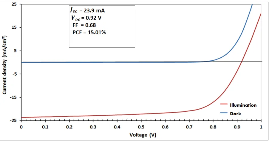
fabricate perovskite thin films for our solar cells to compare with their PCEs. Figure 7 shows
J-V characteristics of solar cells produced with different MAI concentrations. Among all
measured characteristics, the best performance was achieved with solar cells produced using
perovskite film made with 1.0 wt.% MAI solution deposited onto the pre-coated PbI2 thin
film. A summary of performance of all PV devices is listed in Table 1. It is shown that solar
cells made with 1.0 wt% MAI concentration have demonstrated typical performance with
PCE of 15.01%, short circuit current of 23.8 mA/cm², and fill factor of 0.70. Such high
performance solar cells were achieved as a result of uniform, homogeneous, and connected
perovskite thin films. Solar cells produced with 1.2 wt% MAI solution exhibited a reduction
in their performance. A low PCE of 6.76% can be ascribed to the low current density of 14.7
mA/cm2 and low FF of 0.5 measured for such devices. The smaller thickness of the
perovskite film obtained from using such MAI concentration may be considered as the main
reason for the low device performance. Furthermore, solar cells produced with perovskite
film from the 0.8 wt% MAI solution have demonstrated the poorest PCE of 4.19%, which is
the consequence of low current density of 11.4 mA/cm2 and very poor FF of 0.38. The high
proportion of the residual PbI2 phase in the perovskite thin film may be considered as the
main culprit for the poor performance. The other reason for such poor performance may be
ascribed to the poor surface coverage of the perovskite film leading to formation of pin holes
and thus short circuit current. All studied perovskite solar cells produced with different MAI
concentrations have demonstrated high open-circuit voltage above 0.9 V.
Figure 8 shows J-V characteristics of perovskit solar cells made with 1.0 wt% MAI solution
measured both in the dark and under illumination of 100 mW cm-2. This particular device has
statistical distribution of performance of 135 solar cells fabricated from the 1.0 wt% MAI
solution, showing excellent reproducibility of perovskite solar cells with high performance.
The influence of hysteresis on our perovskite solar cells is also investigated in the current
work. Figure 10 shows J-V measurements of perovskit solar cells made with 1.0 wt% MAI
solution scanned in forward and reverse bias directions, where the phenomenon of hysteresis
is considered as one of main concerns in the stability of perovskite-based solar cells [34]. Our
solar cells exhibited convergent performance in PCE under both forward and reverse scan
directions, suggesting almost negligible hysteresis effect. This is credited to the reduction in
the density of defects due to the controlled morphologies of our perovskite films by the
two-step fabrication method [34]. The decent interface between the perovskite layer and the
electron or hole transport layers can be another reason for the mitigation of the hysteresis
effect in the perovskite solar cells [35].
4. Conclusion
The low-temperature two-step fabrication method was used to produce the high quality
CH3NH3PbI3 thin films for PHJ solar cells. It was found that concentration of the MAI
solution and reaction time between MAI and PbI2 have a significant impact on the
morphologies and crystal growth of the perovskite thin films. Highly reproducible perovskite
thin films were fabricated for solar cells application when 1.0 wt% MAI solution was applied
to preformed PbI2 films. Among 110 solar cells from the best perovskite films made with the
1.0 wt.% MAI solution and one minute reaction time about one third have exhibited an
average performance with PCE of 13.63 % while the highest achieved PCE was of 15.01%.
Acknowledgements
The authors would like to acknowledge the facility support by Sheffield Hallam University
References
[1] Y. Hou, H. Zhang, W. Chen, S. Chen, C. O. R. Quiroz, H. Azimi, A. Osvet, G. J. Matt,
E. Zeira, J. Seuring, N. K. Busies, W. Lövenich and C. J. Brabec, Inverted, Environmentally
Stable Perovskite Solar Cell with a Novel Low‐Cost and Water‐Free PEDOT Hole‐
Extraction Layer. Adv. Energy Mater. 5, 1500543 (2015)
[2] C. Bi, Y. Shao, Y. Yuan, Z. Xiao, C. Wang, Y. Gao and J. Huang, Understanding the
formation and evolution of interdiffusion grown organolead halide perovskite thin films by
thermal annealing. J Mater Chem A. 2, 18508-18514 (2014)
[3] K. G. Lim, H. B. Kim, J. Jeong, H. Kim, J. Y. Kim and T. W. Lee, Boosting the Power
Conversion Efficiency of Perovskite Solar Cells Using Self‐Organized Polymeric Hole
Extraction Layers with High Work Function. Adv. Mater. 26, 6461-6466 (2014)
[4] H. Zhang, H. Azimi, Y. Hou, T. Ameri, T. Przybilla, E. Spiecker, M. Kraft, U. Scherf,
and C. J. Brabec, Improved high-efficiency perovskite planar heterojunction solar cells via
incorporation of a polyelectrolyte interlayer. Chem. Mater. 26, 5190-5193 (2014)
[5] G. Xing, N. Mathews, S. Sun, S. Lim, Y. Lam, M. Grätzel and S. Mhaisalkar,
Long-range balanced electron-and hole-transport lengths in organic-inorganic CH3NH3PbI3.
Science. 342, 344-347 (2013)
[6] S. A. Kulkarni,T. Baikie, P. P. Boix, N. Yantara, N. Mathews and S. G. Mhaisalkar,
Band-gap tuning of lead halide perovskites using a sequential deposition process. J Mater
[7] J. H. Noh, S. H. Im, J. H. Heo, T. N. Mandal and S. I. Seok, Chemical management for
colorful, efficient, and stable inorganic–organic hybrid nanostructured solar cells. Nano Lett.
13, 1764-1769 (2013)
[8] A. Kojima, K. Teshima, Y. Shirai and T. Miyasaka, Organometal halide perovskites as
visible-light sensitizers for photovoltaic cells. J. Am. Chem. Soc. 131, 6050–6051 (2009)
[9] M. Tavakoli, D. Bi, L. Pan, A. Hagfeldt, S. Zakeeruddin and M. Grätzel, Adamantanes
Enhance the Photovoltaic Performance and Operational Stability of Perovskite Solar Cells by
Effective Mitigation of Interfacial Defect States. Adv. Energy Mater. 1800275 (2018)
[10] S. Karuppuchamy, G. Murugadoss, K. Ramachandran, V. Saxena, R. Thangamuthu,
Inorganic based hole transport materials for perovskite solar cells. J. Mater. Sci. Mater.
Electron. 29(10), 8847–8853 (2018)
[11] K. Wojciechowski, M. Saliba, T. Leijtens, A. Abate and H. J. Snaith,Sub-150 C
processed meso-superstructured perovskite solar cells with enhanced efficiency. ENERG
ENVIRON SCI. 7, 1142-1147 (2014)
[12] J. T. Wang, J. M. Ball, E. M. Barea, A. Abate, J. A. A. Webber and J. Huang, M.
Saliba, I. Mora-Sero, J. Bisquert, H. J. Snaith, R.J. Nicholas, Low-temperature processed
electron collection layers of graphene/TiO2 nanocomposites in thin film perovskite solar
cells. Nano Lett. 14, 724-730 (2013)
[13] P. Qin, A. L. Domanski, A. K. Chandiran, R. Berger, H. J. u. Butt, M. I. Dar, T.
Moehl, N. Tetreault, P. Gao, S. Ahmad, M. K. Nazeeruddin and M. Gratzel,
Yttrium-substituted nanocrystalline TiO 2 photoanodes for perovskite based heterojunction solar cells.
[14] J. W. Lee, S. H. Lee, H. S. Ko, J. Kwon, J. H. Park, S. M. Kang, N. Ahn, M. Choi, J. K.
Kim and N. G. Park, Opto-electronic properties of TiO 2 nanohelices with embedded HC
(NH 2) 2 PbI 3 perovskite solar cells. J Mater Chem A. 3, 9179-9186 (2015)
[15] N. G. Park, Organometal perovskite light absorbers toward a 20% efficiency low-cost
solid-state mesoscopic solar cell. J. Phys. Chem. Lett. 4, 2423-2429 (2013)
[16] J. H. Kim, C. C. Chueh, S. T. Williams and A. K. Y. Jen, Room-temperature,
solution-processable organic electron extraction layer for high-performance planar heterojunction
perovskite solar cells. nanoscale.7, 17343-17349 (2015)
[17] S. Ryu, J. Seo, S. S. Shin, Y. C. Kim, N. J. Jeon, J. H. Noha and S. I. Seok.
Fabrication of metal-oxide-free CH 3 NH 3 PbI 3 perovskite solar cells processed at low
temperature. J Mater Chem A. 3, 3271-3275 (2015)
[18] C. H. Chiang, Z. L. Tseng and C. G. Wu, Planar heterojunction perovskite/PC 71 BM
solar cells with enhanced open-circuit voltage via a (2/1)-step spin-coating process. J Mater
Chem A . 2, 15897-15903 (2014)
[19] J. Duan, Q. Xiong, H. Wang, J. Zhang and J. Hu, ZnO nanostructures for efficient
perovskite solar cells. J. Mater. Sci.: Mater. Electron. 28, 60 (2017)
[20] J. Seo, S. Park, Y. C. Kim, N. J. Jeon, J. H. Noh, S. C. Yoon and S. I. Seok, Benefits
of very thin PCBM and LiF layers for solution-processed p–i–n perovskite solar cells.
ENERG ENVIRON SCI. 7, 2642-2646 (2014)
[21] L. Zheng, D. Zhang, Y. Ma, Z. Lu, Z. Chen, S. Wang, L. Xiao, Q. Gong, Morphology
[22] S. Shi, Y. Li, X. Li, H. Wang, Advancements in all-solid-state hybrid solar cells based
on organometal halide perovskites. Mater Horizons. 2, 378-405 (2015)
[23] Chen Q, Zhou H, Hong Z, S. Luo, H. S. Duan, H. H. Wang, Y. Liu, G. Li, Y. Yang,
Planar heterojunction perovskite solar cells via vapor assisted solution process. J Am Chem
Soc. 136, 622-625 (2013)
[24] Jiang M, Wu J, Lan F, Q. Tao, D. Gao, G. Li, Enhancing the performance of planar
organo-lead halide perovskite solar cells by using a mixed halide source. J Mater Chem A. 3,
963–967 (2015)
[25] Hao F, C. C. Stoumpos, Z. Liu, R. P. Chang, M. G. Kanatzidis, Controllable
perovskite crystallization at a gas–solid interface for hole conductor-free solar cells with
steady power conversion efficiency over 10%. J Am Chem Soc. 136, 16411–16419 (2014)
[26] Zhao Y, Zhu K, Solution Chemistry Engineering toward High-Efficiency Perovskite
Solar Cells. J Phys Chem Lett 5, 4175–4186 (2014)
[27] D. Shi, V. Adinolfi, R. Comin, , M. Yuan, E. Alarousu, A. Buin, Y. Chen, S.
Hoogland, A. Rothenberger, K. Katsiev, Y. Losovyj, Low trap-state density and long carrier
diffusion in organolead trihalide perovskite single crystals. Science . 347, 519-522 (2015)
[28] Huang H, Shi J, L. Zhu, D. Li, Y. Luo, Q. Meng, Two-step ultrasonic spray
deposition of CH3NH3PbI3 for efficient and large-area perovskite solar cell. Nano Energy.
27, 352-358 (2016)
[29] H. L. Hsu, C. P. Chen, J. Y. Chang, Y. Y. Yu, Y. K. Shen, Two-step thermal
annealing improves the morphology of spin-coated films for highly efficient perovskite
[30] Z. Xiao, Q. Dong, C. Bi, Y. Shao, Y. Yuan, J. Huang, Solvent Annealing of
Perovskite-Induced Crystal Growth for Photovoltaic-Device Efficiency Enhancement. Adv
Mater. 26, 6503-6509 (2014)
[31] Y. Chen, T. Chen, L. Dai, Layer-by-Layer Growth of CH 3 NH 3 PbI 3− x Cl x for
Highly Efficient Planar Heterojunction Perovskite Solar Cells. Adv Mater. 27, 1053-1059
(2015)
[32] Y. Zhao, K. Zhu, Solution Chemistry Engineering toward High-Efficiency Perovskite
Solar Cells. J Phys Chem Lett. 5, 4175-4186 (2014)
[33] J. Qiu, Y. Qiu, K. Yan. M. Zhong, C. Mu, H. Yan, S. Yang, All-solid-state hybrid solar
cells based on a new organometal halide perovskite sensitizer and one-dimensional TiO 2
nanowire arrays. Nanoscale 5, 3245 (2013)
[34] H. J. Snaith, A. Abate, J. M. Ball, G. E. Eperon, T. Leijtens, N. K. Noel, S. D. Stranks, J.
T. W. Wang, K. Wojciechowski, W. Zhang, Anomalous hysteresis in perovskite solar cells. J.
Phys. Chem. Lett. 5, 1511–1515 (2014)
[35] G. E. Eperon, V. M. Burlakov, A. Goriely , H. J. Snaith. Neutral color semitransparent
Table 1 Device performance against varied concentrations of the MAI solution
Concentration of MAI (wt%)
Voc
(V)
Jsc
(mA/cm²)
FF PCE
(%)
0.8 0.95 11.4 0.38 4.19
1 0.92 23.8 0.70 15.01
Figure 2: A schematic diagram of the processing model for the formation of perovskite thin
Figure 5: UV-Vis absorption spectra of CH3NH3PbI3 films with different MAI concentrations
Figure 6: X-ray diffraction patterns of CH3NH3PbI3 solar cells with different MAI
[image:27.595.71.528.72.344.2]Figure 7: J-V performances of the perovskite solar cells with different MAI concentrations
[image:28.595.75.527.101.341.2]Figure 8: J-V performances for the best solar cell under illumination and dark conditions,
[image:29.595.73.524.69.305.2]respectively.
Figure 9: the performance distribution of 135 solar cells fabricated from the 1.0 wt% MAI
[image:29.595.77.523.395.635.2]