Wright State University Wright State University
CORE Scholar
CORE Scholar
Browse all Theses and Dissertations Theses and Dissertations
2014
6 GHz RF CMOS Active Inductor Band Pass Filter Design and
6 GHz RF CMOS Active Inductor Band Pass Filter Design and
Process Variation Detection
Process Variation Detection
Shuo Li
Wright State University
Follow this and additional works at: https://corescholar.libraries.wright.edu/etd_all Part of the Electrical and Computer Engineering Commons
Repository Citation Repository Citation
Li, Shuo, "6 GHz RF CMOS Active Inductor Band Pass Filter Design and Process Variation Detection" (2014). Browse all Theses and Dissertations. 1386.
https://corescholar.libraries.wright.edu/etd_all/1386
This Thesis is brought to you for free and open access by the Theses and Dissertations at CORE Scholar. It has been accepted for inclusion in Browse all Theses and Dissertations by an authorized administrator of CORE Scholar. For more information, please contact [email protected].
6 GHz RF CMOS Active Inductor Band Pass Filter Design and
Process Variation Detection
A thesis submitted in partial fulfillment
of the requirements for the degree of
Master of Science in Engineering
By
SHUO LI
B.S., Dalian Jiaotong University, China, 2012
2014
WRIGHT STATE UNIVERSITY GRADUATE SCHOOL
July 1, 2013 I HEREBY RECOMMEND THAT THE THESIS PREPARED UNDER MY SUPERVISION BY Shuo Li ENTITLED “6 GHz RF CMOS Active Inductor Band Pass Filter Design and Process Variation Detection” BE ACCEPTED IN PARTIAL FULFILLMENT OF THE REQUIREMENTS FOR THE DEGREE OF Master of Science in Engineering ___________________________ Saiyu Ren, Ph.D. Thesis Director ___________________________ Brian D. Rigling, Ph.D. Chair, Department of Electrical Engineering
Committee on Final Examination ___________________________ Saiyu Ren, Ph.D. ___________________________ Raymond Siferd, Ph.D. ___________________________ Yan Zhuang, Ph.D. ___________________________ Robert E. W. Fyffe, Ph.D. Vice President for Research and
Abstract
Li, Shuo. M.S.Egr, Department of Electrical Engineering, Wright State University, 2014. “6 GHz RF CMOS Active Inductor Band Pass Filter Design and Process Variation Detection”
A 90nm CMOS active inductor band pass filter with automatic peak detection is
demonstrated in this thesis. The active inductor band pass filter has a better performance
than the passive band pass filter in on-chip circuit design, due to small area, larger gain
and tunable frequency. However, process variation makes the active inductor band pass
filter hard to be used widely in many applications. To settle this issue, an automatic
voltage peak detector is introduced to detect the process variation direction and hope to
be used to control the active inductor band pass filter center frequency and gain. The
designed active filter shows center frequency of 6GHz and quality factor (Q) of 31.9.
To drive the peak detector, two analog buffers are designed with f-dB over 6GHz, and
one has 0dB gain at low frequency region, another one would emphasize 0dB gain on
6GHz. The voltage peak detector can detect the AC input amplitude range from 0.06V
iv
Table of Contents
I. Introduction ... 1 1.1 Passive Filters ... 1 1.2 CMOS Technology ... 3 1.3 PVT Variation ... 4 1.3.1 Process Variation ... 5 1.3.2 Voltage Variation ... 5 1.3.3 Temperature Variation ... 61.4 Active Inductor Band Pass Filter ... 6
1.5 Analog Buffer ... 7
1.6 Voltage Peak Detector ... 8
1.7 Motivation ... 8
1.8 Objective ... 9
II. CMOS Active Band Pass Filter ...11
2.1 Gyrator-C Active Inductor Implementation ...11
2.2 Active Inductor Band Pass Filter ...12
2.3 Simulation results ...15
2.4 Manual Calibration ...20
III. Analog Buffer ...22
3.1 System Review ...22
3.2 Circuit Architecture ...23
3.3 Practical Circuit Design and Simulation Results ...30
3.3.1 Transistor Width Set Up ...30
3.3.2 Simulation Result ...31
3.4 Summary ...35
IV. CMOS Peak Detector ...37
4.1 Circuit Implementation ...37
4.2 Simulation Results...38
4.3 Circuit Modification ...40
4.4 Output Continuous Detection with Input Amplitude Change ...45
4.5 Circuit Summary ...46
V. On-chip CMOS Active Band Pass Filter with Amplitude Detection ...47
5.1 Circuit introduction ...47
5.2 Automatic Amplitude Detector Simulation Result ...48
6.1 Conclusion ...50
6.2 Future works ...51
List of Figures
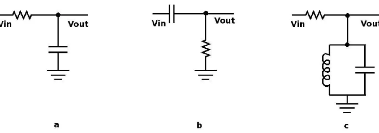
Fig 1.1.1 Three filters circuit diagrams: (a) Low pass filter (b) High pass filter (c) Band pass filter
... 2
Fig 1.1.2 Three filters function diagrams: (a) Low pass filter (b) High pass filter (c) Band pass filter ... 2
Fig 1.2.1 NMOS and PMOS (from left to right) schematic symbol ... 4
Fig 2.1.1 Gyrator-C network ...11
Fig 2.2.1 Active Inductor Based BP Filter ...13
Fig 2.3.1 AC analysis of active band pass filter ...15
Fig 2.3.2 Transient analysis of active inductor band pass filter ...16
Fig 2.3.3 Corner analysis output center frequency (split) ...17
Fig 2.3.4 Corner analysis output center frequency (combined) ...17
Fig 2.3.5 Monte Carlo analysis with mismatch data saved (run 20 times) ...19
Fig 2.4.1 FF corner ac simulation after manual adjustment ...20
Fig 2.4.2 SS corner ac simulation after manual adjustment ...21
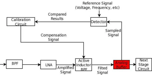
Fig 3.1.1 Block diagram of automatically calibrated active inductor band pass filter. ...22
Fig 3.2.1 Current sink analog buffer. ...23
Fig 3.2.2 AC signal equivalent circuit of current sink analog buffer ...24
Fig 3.2.3 NMOS transistor 3D diagram ...24
Fig 3.2.4 Schematic diagram of proposed analog buffer. ...28
Fig 3.2.5 AC signal equivalent circuit of the proposed analog buffer. ...28
Fig 3.3.1 Bode plot of referenced and proposed buffer : (a) one-side analog buffer; (b) low gain proposed analog buffer; (c) high gain proposed analog buffer. ...32
Fig 3.3.2 Comparison of referenced and proposed buffer time domain working performance: (a) one-side analog buffer; (b) low gain proposed analog buffer; (c) high gain proposed analog buffer. ...34
Fig 4.1.1 Schematic of CMOS peak detector ...37
Fig 4.2.1 CMOS peak detector simulation results with input amplitude equal to 0.1V (Red/Top), 0.2V (Yellow/Middle), and 0.3V (Green/Bottom). ...39
vi
Fig 4.2.2 11 output samples DC value with input amplitude from 0.1V to 0.3V. ...40
Fig 4.3.1 Modified CMOS peak detector schematic. ...41
Fig 4.3.2 Simulation waveform of modified CMOS peak detector ...42
Fig 4.3.3 Simulation results line diagram of modified peak detector ...42
Fig 4.3.4 Waveform of low output voltage CMOS peak detector ...43
Fig 4.3.5 Large output range CMOS analog peak detector output data curve. ...44
Fig 4.3.6 0mV-10mV peak detector testing result ...44
Fig 4.4.1 CMOS peak detector with 2-to-1 MUX ...45
Fig 4.4.2 Simulation results with input signal amplitude changing from 0.1V to 0.2V ...46
Fig 5.1.1 Active inductor band pass filter integrated with CMOS analog buffer and CMOS peak detector block diagram ...47
Fig 5.2.1 TT process corner circuit detection results ...48
Fig 5.2.2 SS process corner circuit detection results ...48
List of Tables
Table 2.3. 1Comparison of corner analysis ... 18 Table 2.3.2 Summary Monte Carlo Analysis ... 19 Table 2.4.1 Transistor’s function of tuning the output waveforms ... 21 Table 3.2.1 90nm theoretical parameter and circuit modulus represented by transistor widths. ... 26 Table 3.2.2 Supportive part’s transistors’ parameters. ... 29 Table 3.3.1 Time domain simulation results of low gain and high design. ... 35
viii
Acknowledgement
I would like to express my deepest gratitude to my thesis advisor: Dr. Saiyu Ren
for her selfless support on my thesis and graduate study during past two years. Her
intelligence, enthusiasm, and concentration on Very Large Scale Integrated Circuit
Design field inspire me all the time. I am thankful that she gives me a chance to be a
member of her research team, and let me learn the most advance technology in CMOS
circuit design.
Besides my advisor, I also want to thank to Dr. Raymond Siferd, who gives me
many constructive advices in my study and research. His wisdom and kindness is the
inexhaustible resource during my study life in Wright State University.
Finally, I would like to thank to Dr. Yan Zhuang for his service as my thesis defense
I. Introduction
State of the art, wireless communication applications are indispensable in all
around the world. GPS system, cellular telephone and other wireless devices are playing
an essential role in people’s daily lives [1].
For wireless applications, receiver system is the vital block. The signals in
atmosphere are detected and received by an antenna or antenna arrays, and passes to
the following low noise amplifier (LNA) stage to amplify the detected signals and filter
out some of the noise. Usually the received signal is weak and noisy, so band pass filters
(BPF) are needed to pass the desired signals in a bandwidth (BW) and attenuate noise
[2]. After the LNA and BPF, the received signals are stronger and less noise, which will
be continued processed by the following receiver chain that is out of the scope of this
thesis
1.1 Passive Filters
There are three types of filters, low pass, high pass and band pass filters. Their
basic implementations are shown in Fig 1.1.1 by using passive components, resistor,
capacitor and inductor. The Bode plot in Fig 1.1.2 shows a low pass filter passes low
frequency signals and block high frequency signals; a high pass filter passes high
frequency signal and attenuate low frequency signals, which is the opposite function of
low pass filter; a band pass filter aims to select a certain frequency range signal and
attenuates signals with frequencies outside this range. A typical passive BPF combines
2
frequency which is the desired input signal frequency with a certain bandwidth.
Fig 1.1.1 Three filters circuit diagrams: (a) Low pass filter (b) High pass filter (c) Band pass filter
(a) (b) (c)
Fig 1.1.2 Three filters function diagrams: (a) Low pass filter (b) High pass filter (c) Band pass filter
The order of a passive filter mainly depends on the number of capacitor and
inductor components in the circuit [3]. For example, the band pass filter shown in Fig
1.1.1 is a 2nd order filter. Based on Fig 1.1.1(c), Ohm’s law, and Kirchoff’s circuit laws
[4], the transfer function of this band pass filter is
𝑉𝑖𝑛 𝑅+𝑆𝐿∗ 1 𝑆𝐶 𝑆𝐿+𝑆𝐶1 ∗𝑆𝐿∗ 1 𝑆𝐶 𝑆𝐿+𝑆𝐶1 = 𝑉𝑜𝑢𝑡 (1.1.1) 𝐻(𝑠) =𝑉𝑜𝑢𝑡𝑉𝑖𝑛 = 𝑆𝑙∗ 1 𝑆𝐶 (𝑆𝐿+𝑆𝐶1)𝑅+𝑆𝐿∗𝑆𝐶1 (1.1.2)
Eq. (1.1.2) can be further simplified to
According to Eq. (1.1.3), the s order would increase when the number of inductive
and capacitive component in circuit getting large. So, for band pass filter design, the
general function is
𝐻(𝑠) =𝑎𝑚𝑠𝑚+𝑎𝑚−1𝑠𝑚−1+𝑎𝑚−2𝑠𝑚−2+⋯𝑎1𝑠+𝑎0
𝑏𝑛𝑠𝑛+𝑏𝑛−1𝑠𝑛−1+𝑏𝑛−2𝑠𝑛−2+⋯𝑏1𝑠+𝑏0 (1.1.4)
Eq. 1.1.4 indicates that higher order design could give designer more space to
optimize filters. However, more passive components would take a lot of the design area,
especially for on-chip application. Thus, the CMOS active inductor band pass filter
technology is essential and potential for today’s chip design and manufactory.
1.2CMOS Technology
CMOS technology has been widely used in very large integrated circuit
implementation for several decades, due to its low power, high density, low cost and
high yield features [5], [6].
The first CMOS circuit was invented in 1963, by Frank Wanlass [6]. After that,
this technology changes the whole world. In today’s life, nearly every electronic equipment employs CMOS technology to operate. CMOS technology include two
MOS transistors, NMOS and PMOS. Each transistor has 4 nodes: drain (D), source (S),
gate (G), and bulk (B) which can also be called body or substrate. Referring to Fig 4,
both NMOS and PMOS transistors are controlled by to-source voltage. When
gate-to-source voltage is greater than NMOS threshold voltage, NMOS is turned on to pass
the current. When gate-to-source voltage is less than PMOS threshold voltage, PMOS
4
Fig 1.2.1 NMOS and PMOS (from left to right) schematic symbol
As CMOS technology is getting more advanced, feature size, transistor size and
cost keep decreasing. Smaller feature size means higher operating speed, and lower
power supply voltage. Thus, the power consumption of each transistor is reduced. For
digital circuit design, low power consumption results in high density of integration.
Intel 15-core Xeon Ivy Bridge-EX CPU integrate 4.3 billion CMOS transistors on a
single chip with 541mm2 area [7], and the system operating clock is up to 3.8 GHz [8].
For analog circuit design, the benefit of smaller feature size is not as good as digital
design, sometimes it brings more trouble. In section 1.3, PVT (Process, Voltage and
Temperature) variation as the biggest drawback of CMOS application will be
introduced.
1.3 PVT Variation
As discussed in Section 1.2, PVT variation is the biggest barrier for many analog
CMOS designs.
Ideally the performance of a fabricated chip should be close to the simulation
results if the circuits are modeled properly. However, in the real world, that is
impossible due to the different manufacture and operating environments, especially for
of a CMOS implementation [9].
1.3.1 Process Variation
No matter how precise the manufacture equipment is, it is not possible to fabricate
two totally identical wafers. Many factors affect the accuracy of wafer production, such
as temperature, pressure and doping concentrations [10]. As a consequence, the
electrical properties like sheet resistance and threshold voltage will be different between
transistors, although they are designed to have exactly same parameters. Such
parameters process variation happens on every element throughout a whole chip, so the
practical result will be departure from expectation, and in many case, this variation is
the key reason of testing failure. Billions of transistors in a same chip experience
process variation, which may cause the chip performance vary substantially from the
theoretical value after fabricating.
There are two methods to analyze the process variation. One is corner analysis,
and another is Monte Carlo analysis. Corner analysis is simulating the different running
speed of circuits assuming all transistors are fabricated at corner process conditions. In
this thesis, three corners are considered which are: TT (Typical NMOS-Typical PMOS),
SS (Slow-Slow) and FF (Fast-Fast) [11]. Monte Carlo analysis assumes a statistical
variation of process parameters and component mismatch.
1.3.2 Voltage Variation
Voltage variation, usually is the supply voltage variation. This variation is caused
by voltage drop of current flowing through the power rail resistors [12] . Since all
currents of the circuit come from the power supply, when this variation happens, the
circuit result will be different with theoretical value. Low power consumption is a
6
scaling down. Such low supply voltage makes the voltage variation more significant,
as the jitter no longer can be ignored compared to the desired rail voltage.
1.3.3 Temperature Variation
Temperature variation cannot be avoided by day-to-day system operating. Every
transistor generates heat to the environment when they are operating. Even though, for
only one transistor, the heat is too small to be noticed, there are billions of transistors
integrated on a single chip and they can easily heat up the surrounding. In the software,
the default operating climate is 27 degree, but in reality, the climate around the chip are
changing all the time. CMOS transistor is a climate sensitive component, which will
lead to the transistor’s speed varying.
To test the temperature variation, ADE XL analysis is used in Cadence software.
In this thesis, 4 temperatures are applied to the circuit to measure the output changing.
They are 0℃, 27℃ (default), 40℃, and 80℃.
1.4 Active Inductor Band Pass Filter
As discussed in 1.1, passive band pass filter is built by passive capacitive and
inductive components. In off-chip design, the passive filter is very popular, since it is
the simplest implementation of a given transfer function. Also, passive band pass filter
can perform the required function without power supply, and the operating frequency
can be very high due to passive components strong tolerance of high current [3]. Also
passive band pass filter generate very little noise compared to active inductor band pass
filter, because the noise of passive filter only comes from resistive components. [3]
However, coming to on-chip integrated circuit design level, the passive band pass filter
has some important disadvantages, such as passive inductor lacks of wide range
difficult. The largest drawback is the extremely large on-chip passive inductor size.
Active CMOS inductors become more and more attractive in recent years. An active
inductor only takes 1-10% the area of a passive inductor with same inductance. [14]
Active CMOS inductor based band pass filter offers a wider frequency tuning range by
adjusting the bias voltage in the circuit. Potential high Q with multiple active filters in
cascaded, and adjustable gain also good for on-chip circuit design. [15] The mainly
concern for the active inductor band pass filter is the PVT variation. Such variation will
vary center frequency, gain and Q factor of active inductor band pass filter from the
desired value which may cause an unacceptable result.
1.5 Analog Buffer
CMOS analog buffer is one of the most important building blocks in mixed signal
design, especially for system on-chip applications [16]. In order to save power and area,
most on-chip applications generate weak internal signal, and only buffered at the output
stage to drive a large capacitive load without distortion [17]. Therefore, the analog
buffer’s input capacitance must be as small as possible to maintain the weak signal the same under different situations [18]. Also, the output of analog buffer needs to have a
large value of slew-rate to meet the requirement of driving a large capacitive load [19].
Previous output buffer designs are mainly focusing on two directions. One is using
the rail-to-rail class AB differential amplifier architecture to reach the low-power and
high slew-rate goals. However, this low-power performance are realized by sacrificing
the frequency. Another type of analog buffer is trying to drive the off-chip low resistive
and high capacitive load. This power amplifier consumes a large amount of power to
complete the driving requirements [20]. The design objective for the analog buffer in
8
frequency with relative low power consumption. This design objective matches the
active inductor filter application as will be discussed later.
1.6 Voltage Peak Detector
Fully automatic calibration process uses the variation information detected by the
detector to determine how to adjust the bias voltage to compensate the CMOS active
inductor band pass filter. To tell the frequency changing, based on simulation data, a
CMOS voltage peak detector is designed in this thesis. When the process variation
happens, active inductor band pass filter center frequency and output amplitude value
will vary to a different value. The peak detector can detect the output amplitude and
convert it to a desired DC feedback voltage value.
For entire calibration block, the number of transistors must be as small as possible,
due to the self process variation. The detection circuit, as the first block of whole
calibration process, has to have as small error caused by the process variation as
possible. Thus, a simple architecture CMOS peak detector is needed in this thesis. There
are many CMOS detector designs, and some of them are very accurate but complicated.
One reported CMOS peak detector uses only two transistors to detect the sine wave
amplitude alteration. In chapter 4, this detector will be analyzed and modified to meet
the design specification.
1.7 Motivation
In information age, most people cannot live without electronic devices.
Televisions, computers, and cell phones are becoming part of peoples’ daily life. Users
always want the device to be smaller, long battery life and more powerful, which
requires every single gate on the chip using less area and having better performance.
chip to filter out unwanted signals. In modern CMOS very large integrated circuit
design, band pass filter is required to have smaller size, higher center frequency and
quality factor, and lower power consumption. In order to satisfy those goals, CMOS
active inductor is implemented to replace the passive inductor. The lower area
consumption and center frequency adjustability make CMOS active inductor band pass
filter a promising on-chip component; however the PVT variation is the biggest
drawback of CMOS circuit. Researchers have been working hard to reduce PVT
variation. With feature size getting smaller, PVT variation is getting larger, and
calibration becomes a must-do procedure to produce a high performance analog CMOS
chip. For a high density integrated circuit, manually calibration is usually impossible.
So, an automatic detecting and calibrating circuit is vital to the on-chip active inductor
band pass filter application.
1.8 Objective
The objective of this thesis to implement a CMOS active inductor band pass filter
function, and be able to detect process variation direction, then calibrate the effect of
PVT variation. The detailed tasks include:
A CMOS active inductor based band pass filter with 6GHz center frequency. The center frequency of the active BPF can be tuned back to 6GHz by
adjusting only bias voltage at all three corners.
A CMOS analog buffer with 0dB DC gain, and 6GHz -3dB frequency is designed to drive peak detector and other circuits after the active filter. A good
driving ability is essential for this analog buffer design, and the input
capacitance needs to be small to minimize its effect to the band pass filter.
10
the CMOS active inductor band pass filter output changes, and reflect signal
II. CMOS Active Band Pass Filter
2.1 Gyrator-C Active Inductor Implementation
Gyrator is first proposed by Bernard D.H. Tellegen in 1948 [21]. It describes a
two-port device using voltage, current, and gyration conductance (G). For CMOS
technology, G represents the conductance of a transistor. Usually,
trans-conductance (gm) is calculated by the ratio of current and voltage, which is the reciprocal of impedance. A gyrator is built by two back-to-back connected
trans-conductors. When one node of the gyrator is connected to a capacitor which in this case
is a varactor, the network can be used to synthesize an inductor as Fig. 2.1.1 shown [22]:
Fig 2.1.1 Gyrator-C network
12
represents the trans-conductance. C is a varactor, and VC means the node voltage of this
varactor. The equivalent impedance of network is derived as follows.
Assume the input voltage is Vin and current is Iin, the input impedance can be developed in Eq. (2.1.1)
Zin= VIin
in (2.1.1)
The input current equals to
Iin = −gm2∗ Vc (2.1.2) At the same time, using gm2 path, the varactor’s node voltage also can be expressed as Eq. (2.1.3)
Vc = −gm1∗ Vin∗sC1 (2.1.3) Thus, the impedance of this gyrator design is
Vin
Iin =
sC
gm1∗gm2 (2.1.4)
Refer to the impedance Z for an inductor is equal to sL, so
Leq =g C
m1∗gm2 (2.1.5)
From Eq. (2.1.5) it can be seen that the inductance of the active inductor is
proportional to the capacitance of varactor, and inversely proportional to gm1 and gm2 which are trans-conductance of transistors.
2.2 Active Inductor Band Pass Filter
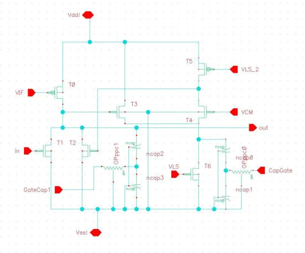
Fig 2.1.2 is the transistor level diagram for an active inductor band pass filter,
where T3, T2 and ncap0&1 are used to implement an active inductor as depicted in
Fig 2.2.1 Active Inductor Based BP Filter
For this design, transistor T0 and T6 is using as current source and current sink. .
Current of T1 transistor (IT1) value depends on current flowing from T0 (IT0) and
gm1 = IT1
Vin(DC), so IT0 will be the dominant factor for varying the inductance when
Vin(DC) is fixed. In other word, the bias voltage of T0 transistor (VIF) can control the inductance of active inductor. Also, since IT1 + IT2 (current of T2 transistor) must equal
to IT0, circuit would automatically adjust the drain node voltage of T0, which is connected to output, to balance the current in this path. Thus IT1 could affect output
offset value, and the bias voltage VIF will have a big effect for further active inductor
band pass filter calibration.
14
active inductor and a varactor to perform band pass function. The center frequency will
be controlled by the output inductance and capacitance based on band pass filter center
frequency equation. Substitute the equivalent inductance of active inductor into center
frequency equation.
𝑓𝑜 =2∗𝜋∗√𝐿∗𝐶1 = 𝑔2∗𝜋∗𝐶𝑚1𝑔𝑚2 (2.2.1)
Another important data to evaluate a band pass filter performance is the quality
factor Q. Q usually describes the ratio of center frequency and 3dB down frequency,
which is also used to measure the “sharpness” of amplitude response. The Q value can
reflect how effectively the band pass filter can enlarge the desired signal and discard
unwanted signals. For active band pass filter, Q can be estimated using the equation
below. Noticed R in Eq. (2.2.2) is the resistance of inductor.
Q =𝑅1√𝐿𝐶 [23] (2.2.2) There are two vectors to change center frequency 𝑓𝑜 and Q of active inductor band pass filter. One is changing output node capacitance (C), and another one is
changing active inductor’s value. The output capacitance is decided by both transistors connected to output node and load capacitance which is related to next stage circuit
input transistors. Once the circuit is placed on chip, all transistors’ size are fixed, and output node capacitance is also fixed. Thus by changing output capacitance cannot
adjust band pass filter’s center frequency.
However, a couple techniques can be used to adjust the active inductance, such as
varying the varactor value by adjusting the control voltage of the varactor, changing the
bias voltage of the transistors to adjust trans-conductance. Based on section 2.1 analysis,
active inductance could be tuned by adjusting varactor or bias voltage value. Using this
specification. Such characteristic makes active inductor more attractable than
traditional on-chip passive inductor whose inductance is non-variable after fabrication.
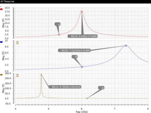
2.3 Simulation results
A one stage active inductor based BP filter is implemented in 90nm CMOS
technology. The schematic circuit is given in Fig. 2.2.1. Simulations are performed in
Cadence Analogue Design Environment (ADE). Fig 2.3.1 indicates this one stage active
inductor band pass filter’s center frequency is 6GHz. Under this center frequency, gain
is 24.84dB and f−3dB bandwidth is 187.93MHz. So, Q=31.9, as Q=BWfo mentioned in section 2.2.
Fig 2.3.1 AC analysis of active band pass filter
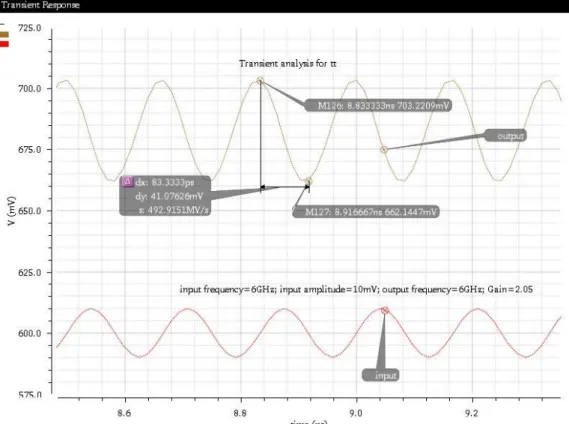
The transient analysis result in Fig 2.3.2 demonstrates the 6GHz output signal has
a gain of 2.05 in linear. This means, the active inductor band pass filter not only can let
the 6 GHz input signal pass through, but also amplify the input signal to make a
16
Fig 2.3.2 Transient analysis of active inductor band pass filter
In introduction part, PVT variation is discussed and illustrated. In this thesis,
corner analysis would be the main method to test the circuit process variation. The TT
(Typical, Typical), FF (Fast, Fast) and SS (Slow, Slow) simulation results are presented
in Fig 2.3.3 and Fig 2.3.4, and the waveform indicates that the circuit center frequency
has a huge variation, varying from 4.78GHz, SS analysis, to 6GHz, TT analysis, to
Fig 2.3.3 Corner analysis output center frequency (split)
Fig 2.3.4 Corner analysis output center frequency (combined)
In Fig 2.3.4, left waveform is produced by active inductor BPF working at SS
corner. Center one is generated at TT corner, and right one is at FF corner. Table 2.3.1
18
parameters, output could vary a lot under different corners. When circuit is in SS corner,
center frequency becomes low, gain and Q raise rapidly, and bandwidth drops
dramatically. On the contrary, in FF corner, center frequency goes high, bandwidth
becomes large, but gain and Q drops.
Table 2.3. 1Comparison of corner analysis
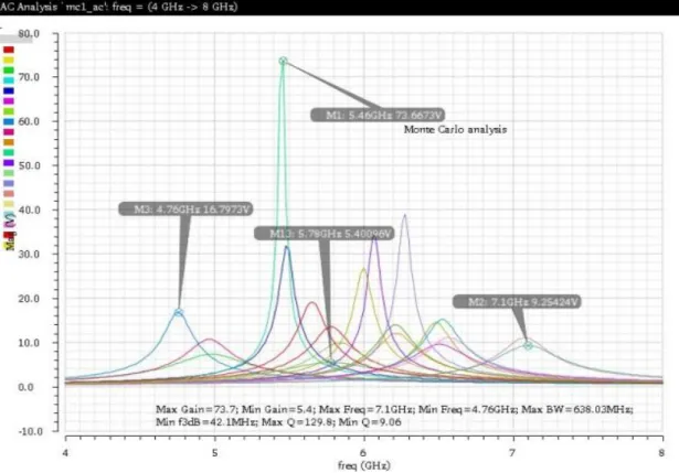
Fig 2.3.5 shows 20 times running simulation waveforms through Monte Carlo
analysis with mismatch data saved. Table 2.3.2 summarizes the variation of main
parameters. Each of this 20 samples gives a different output data. With such variation,
it is hard for designer to estimate the result, also it’s hard for whole system working with this unstable component.
Corner Center Frequency(GHz) f−3dB bandwidth(MHz) Gain Q TT 6 187.93 17.5 31.9 SS 4.78 10.87 237 440 FF 7.33 469.24 8.3 15.6
Fig 2.3.5 Monte Carlo analysis with mismatch data saved (run 20 times)
Table 2.3.2 Summary Monte Carlo Analysis
Parameter Value Different percentage with TT data (%)
Gain (Max) 73.7 +388.6
Gain (Min) 5.4 -69.1
Center Frequency (Max) 7.1GHz +18.3
Center Frequency (Min) 4.76GHz -20.7
f−3dB Bandwidth (Max) 638.03MHz +239.5
f−3dB Bandwidth (Min) 42.1MHz -77.6
Q Factor (Max) 129.8 +306.9
Q Factor (Min) 9.06 -72.6
Such variation happens nearly in all analog circuits. With these changing
parameters, this active inductor band pass filter couldn’t be used in practical circuits.
In the following part, some manual adjustments of bias voltages are employed to tune
20
2.4 Manual Calibration
The basic idea for manual calibration is changing bias voltages of active inductor
band pass filter shown in Fig 2.1.2 to vary inductance of active inductor. Based on Eq.
(2.1.5), the changing of trans-conductance and internal varactor capacitance could lead
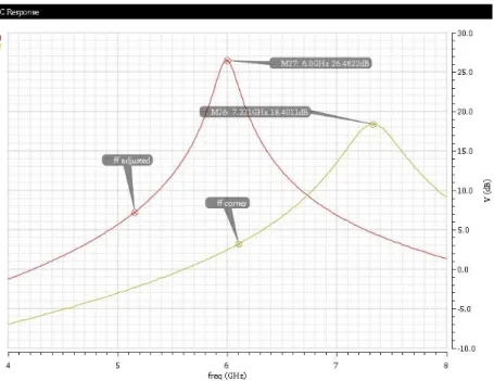
to the changing of active inductance. Fig 2.4.1 is the ac waveform of FF corner
simulation after adjusting the bias voltages of transistors. In this case, VLS the bias
voltage for current sink I5 is increased from 0.6V to 0.7V. VIF which is bias voltage
for generating Ib is increased from 0.6V to 0.618V. The result indicates that center frequency goes down to 6GHz, gain = 26.48dB (21.1), f−3dB bandwidth = 196.45MHz, and Q = 30.54. These data verify that this calibration works by comparing with TT
simulation results. In Fig 2.4.1, right waveform indicates BPF center frequency before
adjustment, and right waveform present the center frequency is brought back to 6GHz.
Fig 2.4.1 FF corner ac simulation after manual adjustment
Using the same technique to calibrate SS situation which is shown in Fig 2.4.2,
from 0.6V to 1V. VCM changes from 0.6V to 0.7V, and VB4 is decreased from 0.6V to 0.46V. VLS goes up from 0.6V to 0.65V, and VIF goes down from 0.6V to 0.59V. The
adjusted waveform center frequency goes up to 6GHz, gain = 14.01dB (5.02), f−3dB bandwidth = 586.82MHz, and Q = 10.22, which are comparable to TT analysis results.
In Fig 2.4.2, left waveform indicates BPF center frequency before adjustment, and right
waveform present the center frequency is brought back to 6GHz.
Fig 2.4.2 SS corner ac simulation after manual adjustment
Table 2.4.1 list the functionality of each individual transistor to the gain, center
frequency and quality factor of active inductor based BP filter in Fig 2.1.2. Based on
this table, the output signal can be manually calibrated to the desired center frequency.
Table 2.4.1 Transistor’s function of tuning the output waveforms
Bias voltage name Function after increase the voltage
VIF fo increase
VLS fo and Q increase
VCM fo and Gain increase
22
III. Analog Buffer 3.1 System Review
The motivation to design this analog buffer is for serving active inductor band pass
filter and calibration circuit. Traditional on-chip band pass filter is built with on-chip
passive spiral inductors; however, the fatal drawback for this component is area costing.
Advantages of the active CMOS inductor based filter include wide tuning range for
center frequencies, potential high Q values with multiple stages of active filter, tunable
gain, and small size [15]. Nevertheless, since the active inductor band pass filter uses
transistor to perform the inductor function, it would be affected by process, voltage and
temperature (PVT) variation. The PVT variation is happening all the time with circuit
running, and it is one of the most frequently factor to cause the circuit performance
degraded or function error. Thus, a calibration circuit is needed to correct the variation
error.
This section of the thesis is focusing on the wide bandwidth analog buffer design,
which is highlighted in Fig 3.1.1. This analog buffer is used to drive a larger capacitive
load which includes a detector or detectors and the following stage circuit, and also to
mitigate the effect to the active inductor band pass filter from the other following
components. To reduce the analog buffer effect to the active inductor BPF, the input
capacitance of this buffer needs to be minimized, which means keeping the input
transistor sizes small.
3.2 Circuit Architecture
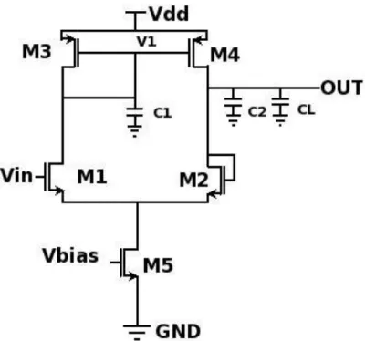
One reported high frequency analog buffer is presented in Fig 3.2.1 [24]. M1 and
M4 transistors are the trans-conductance stages, which transfer the voltage signal to
current signal. M3 transistor is the load stage with load trans-conductance
approximately 𝑔𝑚3, since 𝑔𝑑𝑠1 and 𝑔𝑑𝑠3 is much smaller than 𝑔𝑚3. The same procedure to get M2 transistor’s conductance equals to 𝑔𝑚2 [25]. The small signal
equivalent circuit is given in Fig.3.
24
Through the first stage small signal model in Fig.3, using nodal equation:
−𝑔𝑚1∗ 𝑣𝑖𝑛(𝑠)= 𝑣1(𝑠)∗ (𝑔𝑚3+ 𝑠𝐶1) (3.2.1)
−𝑔𝑚4∗ 𝑣1(𝑠) = 𝑣𝑜𝑢𝑡(𝑠)∗ [𝑔𝑚2+ 𝑠(𝐶2+ 𝐶𝐿)] (3.2.2)
C1 is the capacitance generated from M1, M3 and M4 transistors at 𝑣1 node, which includes Cgd1, Cdb1, Cgs3 and Cgs4, meanwhile the output node’s capacitance
𝐶2 = 𝐶𝑔𝑠2+ 𝐶𝑑𝑏2+ 𝐶𝑔𝑑4+ 𝐶𝑑𝑏4.
Fig 3.2.2 AC signal equivalent circuit of current sink analog buffer
Cgs, Cgd and Cdb are the gate to drain, gate to source and drain to bulk
capacitance for a single transistor, respectively. These capacitance can be estimated
using equations from Eq. (3.2.3) to Eq. (3.2.5) in the following content. The dimensions
in the equations Eq. (3.2.3) to Eq. (3.2.5) are demonstrated in Fig. 3.2.3.
Fig 3.2.3 NMOS transistor 3D diagram
means the length of N type diffusion, and this is a constant value for a specify
technology. There are three equations to estimate list below to estimate gate-to-source,
gate-to-drain, and drain-to-bulk capacitance of single transistor.
Cgs =23Cox∗ W ∗ L + CGSO ∗ W (3.2.3) Cgd = CGDO ∗ W (3.2.4) Cdb= CJ∗A (1+VdBPB)MJ+ CJSW∗P (1+PBSWVdB )MJSW (3.2.5)
For 90nm CMOS technology, 𝐶𝑜𝑥 in Eq. (3.2.3) is oxide capacitance, and it
equals to ε0 ∗ εr/tox, 𝜀0 is permittivity of free space which is 3.9 in here, and 𝜀𝑟
represent the permittivity of silicon dioxide, and its value is 8.85 ∗ 10−18 𝐹/𝑢𝑚. When the oxide thickness 𝑡𝑜𝑥 = 2.05 ∗ 10−9 𝑚, 𝐶𝑜𝑥 is estimated to be 15.97 fF/um2. CGSO in Eq. (3.2.3) and CGDO in Eq. (3.2.4) are gate-source and gate-drain overlap
capacitance, and in this thesis, they have the same value, equal 0.18 fF/um for both
PMOS and NMOS transistors. A and P in Eq. (3.2.5) represent the area and perimeter
of transistors, and A = W*LDiff, P = 2*(W+ LDiff). Choose the diffusion length (LDiff) to
be 0.32um. So, the area for each transistor is (0.32*W) 𝑢𝑚2, and the perimeter is (0.64+2W) um. Substitute all the other parameter values, which cannot be published,
into Eq. (3.2.3), Eq. (3.2.4) and Eq. (3.2.5), the results are summarized in Table.1. Some
small constant value are ignored in the calculation to get the relationship between
transistor capacitance with its width. Based on the data in Table.1, it’s easy to tell that all the capacitance are proportional to width.
DC analysis for the circuit in Fig 3.2.1, all transistors should be operating in
saturation region. M1 and M3 transistors have the same amount of current. M3 and M4
form a current mirror, so IM4= IM3∗ W4/W3 = IM1∗ W4/W3. M2 transistor and
26
transistors all comes from the current generated in M5, so IM5= IM1+ IM1∗ W4/W3,
IM1= IM5/(1 + W4/W3). Source current IM5 is decided by M5 transistor width and
bias voltage. To keep the analog buffer has enough gain, M5 size and bias voltage
should be large. In this thesis, pick W5=40um, and Vbias=0.6V. Thus,
IM5 = 0.5Kn∗ (W5/L) ∗ (Vgs5− Vthn)2 (3.2.6)
Through Cadence simulation analysis results in 90nm CMOS technology, NMOS
transistor’s process gain factor Kn = 86.62 uA/V2, and V
thn= 0.25V are chosen to
be NMOS transistor’s gate threshold voltage for further estimation. So,
IM5= 17324 ∗ (Vbias− 0.25)2 uA (3.2.7)
Based on the trans-conductance equation:
gm = √0.5K ∗ (W/L) ∗ IDSQ (3.2.8)
Table 3.2.1 90nm theoretical parameter and circuit modulus represented by transistor widths. 𝐶𝑔𝑠(𝑛,𝑝) 1.271*W fF 𝐶𝑔𝑑(𝑛,𝑝) 0.18*W fF 𝐶𝑑𝑏𝑛 0.327*W fF 𝐶𝑑𝑏𝑝 0.343*W fF 𝐶1 (0.507W1+1.271W3+1.451W4) fF 𝐶2 (1.598W2+0.523W4) fF 𝐶𝐿 50 fF 𝑔𝑚1 866.2*(Vbias− Vthn)2*√W1∗W3∗W5W3+W4 uA/V 𝑔𝑚2 866.2*(Vbias− Vthn)2*√W2∗W4∗W5W3+W4 uA/V 𝑔𝑚3 866.2*(Vbias− Vthn)2*W3*√W3+W4W5 uA/V 𝑔𝑚4 866.2*(Vbias− Vthn)2*W4*√W3+W4W5 uA/V
Apply Eq. (3.2.1) into Eq. (3.2.2) then
𝑣𝑜𝑢𝑡(𝑠)= 𝑔𝑚4𝑔𝑚1𝑣𝑖𝑛(𝑠)
(𝑔𝑚3+𝑠𝐶1)(𝑔𝑚2+𝑠(𝐶2+𝐶𝐿)) (3.2.9)
The voltage gain transfer function is,
𝐴𝑣(𝑠)= 𝑣𝑜𝑢𝑡(𝑠)
𝑣𝑖𝑛(𝑠) =
𝑔𝑚1𝑔𝑚4
(𝑔𝑚3+𝑠𝐶1)(𝑔𝑚2+𝑠(𝐶2+𝐶𝐿)) (3.2.10)
The DC voltage gain is when the s in Eq. (3.2.10) equal to 0,
Av(0) =ggm1gm4 m2gm3= W4√W1W3W5W3+W4∗√W3+W4W5 W3√W2W4W5W3+W4∗√W3+W4W5 = W4√W1W3 W3√W2W5 (3.2.11)
Another important parameter for analog buffer design is the 3dB down frequency.
The Eq. (3.2.11) can be expressed in the following equation:
𝐴𝑣(𝑠)= 𝑔𝑚1𝑔𝑚4 𝑔𝑚2𝑔𝑚3∗ 1 (1+𝑠 𝐶1 𝑔𝑚3) ∗ 1 (1+𝑠𝐶2+𝐶𝐿𝑔𝑚2 ) (3.2.12)
Therefore, this analog buffer has two poles, |𝑝1| = 𝑔𝑚3/𝐶1 and |𝑝2| =
𝑔𝑚2/(𝐶2+ 𝐶𝐿). So, at 𝑣1 node:
𝜔1 = |𝑝1| =
866.2∗(𝑉𝑏𝑖𝑎𝑠−𝑉𝑡ℎ𝑛)2∗𝑊3∗√𝑊3+𝑊4𝑊5
(0.507𝑊1+1.271𝑊3+1.451𝑊4) (3.2.13)
And at output node:
𝜔𝑜𝑢𝑡 = |𝑝2| =866.2∗(𝑉𝑏𝑖𝑎𝑠−𝑉𝑡ℎ𝑛)
2∗√𝑊2∗𝑊4∗𝑊5 𝑊3+𝑊4
(1.598𝑊2+0.523𝑊4+50) (3.2.14)
In order to have unity gain, 𝑔𝑚4𝑔𝑚1 should equal to 𝑔𝑚3𝑔𝑚2 from Eq. (3.2.11).
At the same time, to extend the -3dB frequency, 𝑔𝑚2 and 𝑔𝑚3 value need to be high enough to make both 𝑓−3𝑑𝐵𝑉1 and 𝑓−3𝑑𝐵𝑜𝑢𝑡 over 6GHz. Based on Eq. (3.2.13) and Eq. (3.2.14), all transistor widths except M5 need to be small to keep the buffer having a
correct function at 6GHz. However, equation Eq. (3.2.11) indicates that if W5 is large,
then W2 must extremely small to have the DC gain be 0dB. Thus it is hard to extend
28
not suitable for very high frequency design.
Fig 3.2.4 Schematic diagram of proposed analog buffer.
To solve this problem, a supportive stage analog buffer is putting forward. Fig
3.2.4 is the schematic diagram of the proposed analog buffer, which employs current
sink and current source analog buffer to improve the performance. To analyze this
analog buffer’s performance, a simplified small signal model is developed in Fig.5.
Fig 3.2.5 AC signal equivalent circuit of the proposed analog buffer.
Based on the Kirchhoff's current law, V1 and V2 node voltages can be expressed
as:
𝑣1(𝑠) = −𝑔𝑚1∗ 𝑣𝑖𝑛(𝑠)/(𝑔𝑚3+ 𝑠𝐶1) (3.2.15)
𝑣2(𝑠)= −𝑔𝑚7∗ 𝑣𝑖𝑛(𝑠)/(𝑔𝑚9+ 𝑠𝐶4) (3.2.16) In Eq. (3.2.16), 𝐶4 = 𝐶𝑔𝑑7+ 𝐶𝑑𝑏7+ 𝐶𝑔𝑠8+ 𝐶𝑔𝑠9, and the capacitance at output node is C2+C3+CL with C3=𝐶𝑔𝑠6+𝐶𝑑𝑏6+𝐶𝑔𝑑8+𝐶𝑑𝑏8. There are two current sources
supply the current to the output, which are 𝑔𝑚4𝑣1 and 𝑔𝑚8𝑣2. The effective resistance of output is 1/(𝑔𝑚2+ 𝑔𝑚6), when ignore the effect of 𝑔𝑑𝑠. Use one side analog buffer
analysis method to study the current source part, then: IM10 = 0.5Kp∗ (W10/L) ∗
(Vsg10− Vthp)2 (3.2.17)
The Kp in Eq. (3.2.17) is PMOS transistor’s process gain factor, and it equals to
44.66uA/V2, and PMOS transistor gate threshold voltage Vthp=0.25V. Apply some other 90nm technology PMOS parameters into Eq. (3.2.3), Eq. (3.2.4), Eq. (3.2.5), and
Eq. (3.2.8), then all the parameters of current source analog buffer can be gotten and
shown in Table 3.2.2.
Table 3.2.2 Supportive part’s transistors’ parameters.
𝐶3 𝐶3 (1.614W6+0.507W8) fF 𝐶4 (0.523W7+1.271W8+1.271W9) fF 𝑔𝑚6 446.6*(Vbias− Vthp)2*√W6∗W8∗W10W8+W9 uA/V 𝑔𝑚7 446.6*(Vbias− Vthp)2*√W7∗W9∗W10W8+W9 uA/V 𝑔𝑚8 446.6*(Vbias− Vthn)2*W8*√W8+W9W10 uA/V 𝑔𝑚9 446.6*(V bias− Vthn)2*W9*√W8+W9W10 uA/V At output node, 𝑉𝑜𝑢𝑡(𝑠) = 𝑉𝑜𝑢𝑡(𝑠)− (𝑔𝑚4𝑣1(𝑠) + 𝑔𝑚8𝑣2(𝑠))/[𝑔𝑚2+ 𝑔𝑚6+ 𝑠(𝐶2 + 𝐶3)](3.2.18) Apply Eq. (3.2.15) and Eq. (3.2.16) into Eq. (3.2.17), the proposed analog buffer’s
voltage transfer function is:
𝐴𝑣(𝑠)= (𝑔𝑔𝑚1𝑔𝑚4 𝑚3+𝑠𝐶1+ 𝑔𝑚7𝑔𝑚8 𝑔𝑚9+𝑠𝐶4) ( 1 𝑔𝑚2+𝑔𝑚6+𝑠(𝐶2+𝐶3+𝐶𝐿)) (3.2.19) When s in Eq. (3.2.19) equals to 0, the dc gain of the proposed analog buffer is:
𝐴𝑣(0) = (𝑔𝑚1𝑔𝑚4 𝑔𝑚3 + 𝑔𝑚7𝑔𝑚8 𝑔𝑚9 ) ∗ 1 𝑔𝑚2+𝑔𝑚6 (3.2.20)
30
In Eq. (3.2.19), there are three poles, which are: |p1| = gm3/C1, |p2| = 𝑔𝑚9/𝐶4, and |p3|=(𝑔𝑚2+ 𝑔𝑚6)/(𝐶2 + 𝐶3 + 𝐶𝐿). So, 𝜔1 = |𝑝1| =866.2∗(Vbias−Vthn) 2∗W3∗√ W5 W3+W4 (0.507W1+1.271W3+1.451W4) (3.2.21) 𝜔2 = |𝑝2| =𝑔𝑚9 𝐶4 = 446.6∗(Vbias−Vthp)2∗W9∗√W8+W9W10 (0.523W7+2.362W8+2.362W9) (3.2.22)
Substitute all the data into |p3|, then the output node pole can be represented by transistors’ width:
866.2∗(Vbias−Vthn)2∗√W2∗W4∗W5W3+W4 +446.6∗(Vbias−Vthp)2∗√W6∗W8∗W10W8+W9
(2.689W2+0.523W4+2.705W6+0.507W8+50) (3.2.23)
Comparing Eq. (3.2.23) with Eq. (3.2.14), there are more transistors coming into
paly to affect the -3dB frequency, which means the proposed analog buffer has more
flexibility to extend the circuit -3dB frequency. Meanwhile, if W2, W3, W6 and W9 are
fixed to maintain the -3dB frequency over 6GHz, then the DC gain can still be adjusted
to 0dB by varying transistor width of M1, M4, M7 and M8. Even more, this proposed
analog buffer can be designed to offer required gain at certain frequency by setting
transistor width appropriately.
3.3 Practical Circuit Design and Simulation Results
3.3.1 Transistor Width Set Up
Based on Eq. (3.2.20), in order to get a higher AV(0), gm1, gm4, gm7 and gm8
should be large, and 𝑔𝑚2, 𝑔𝑚3, 𝑔𝑚6 and 𝑔𝑚9 should be small. As the trans-conductance of each transistor equals to √2 ∗ 𝐾(𝑛 𝑜𝑟 𝑝)∗𝑊
𝐿 ∗ 𝐼𝑄, and K(n or p) is
this proposed analog buffer design, the quiescent current is generated from both current
sink (M5) and current source (M10), so IQ is a fixed value with parameters of current sink and source unchanged in all test cases. In this way, increasing M1, M4, M7 and
M8 transistor width and decreasing M2, M3, M6 and M9 transistors width can improve
𝐴𝑣(0). Coming into AC analysis, reducing M2, M3, M6 and M9 transistor width will make f−3dB smaller, but also bring C2 and C3 smaller due to the capacitance is
proportional to transistor width. In general, the cutoff frequency would not be affected
too much by altering the width of M2 and M6 transistors. M3 and M9 transistors size
cannot be too small, since 𝑔𝑚3 and 𝑔𝑚9 decide V1 and V2 node f-3dB frequency as
shown in Eq. (3.2.14) and Eq. (3.2.23).
As the statement in system review part, the active inductor band pass filter is lack
of driving ability, so the input transistor width must be small enough to prevent the
input capacitance distorting the output waveform of previous stage’s filter. Therefore, M1 and M7 transistors must have a small size.
As analyzed in chapter 2, process variation has a big effect on the active inductor
band pass filter. Referring data from Table 2.3.1, the center frequency is moved from
4.78GHz in SS corner analysis to 7.33GHz in FF corner analysis. Also, the gain is
changed from lowest 8.3 to highest 237. This indicate the input of the analog buffer
will be varied in a certain range. Thus, the analog buffer should have sufficient input
amplitude and frequency range. For this design, the input amplitude range is 0.1V to
0.3V, and the frequency range is 4.5GHz to 7.5GHz.
3.3.2 Simulation Result
This part presents two groups of testing results by simulating the proposed analog
buffer. One is having 0dB at low frequency, another one increases the gain at low
32
transistors’ width, and both of them have over 6GHz bandwidth.
Fig 3.3.1 is the bode plot for frequency domain simulation of one side, low gain
proposed and high gain proposed analog buffer. The ac results show that the gain is
decreasing with the growth of frequency.
Fig 3.3.1 Bode plot of referenced and proposed buffer : (a) one-side analog buffer; (b) low gain proposed analog buffer; (c) high gain proposed analog buffer.
In low frequency region, the low gain proposed analog buffer supply nearly 0dB
gain to the output, which is -56.9mdB, and the high gain design has 2.17dB, but the one
side analog buffer in Fig.2 has -4.72dB loss during this low frequency range. When the
input frequency goes up to 6GHz, the output gain of proposed high gain analog buffer
is -798mdB, which is a slightly loss. This is much more than the -6.9dB loss of one side
analog buffer. For low gain proposed buffer, the output has -3.05dB loss at 6GHz,
which is not good, but still acceptable to this design. At the required 7.5GHz point, the
proposed high gain analog buffer outputs a -2.3dB loss, but is still acceptable for next
stage detectors to tell the error. However, output signal strength of the low gain
proposed analog buffer and one side analog buffer is only -4.3dB and -7.9dB of the
input, and it adds more difficulties to implement the detection circuit since the detector
needs a very high resolution to tell the difference.
The time domain analysis waveform in Fig 3.3.2 gives a straight forward picture
about the performance increment. The one side analog buffer’s output is distorted when input amplitude is 0.1V and frequency is 6GHz, but at the same testing environment,
both of the low gain and high gain proposed analog buffer tracks the input very well.
The high gain proposed analog buffer has the best performance among this three design,
34
Fig 3.3.2 Comparison of referenced and proposed buffer time domain working performance: (a) one-side analog buffer; (b) low gain proposed analog buffer; (c) high gain proposed analog buffer.
Other time domain simulation data are shown in Table.2, and the result has a
slightly difference with the frequency domain outcome. The results of high gain
proposed analog buffer can work at required input cases, and output sufficient signal
frequency range is included in the input dynamic range of analog buffer. The low gain
proposed analog buffer has a very stable unity gain output at low frequency region, but
doesn’t fit the requirements shown above. If other application working in low frequency, then this low gain analog buffer can be a good option to enhance the design driving
ability. Furthermore, the low gain analog buffer consumes less power than the high gain
design. The advantage of the proposed analog buffer design is the freedom to adjust the
performance. More transistors involved in the output performance makes this proposed
analog buffer offer more special functions than many previous design. Besides, this
proposed analog buffer are mainly focusing on the high frequency on-chip design, so it
has a larger bandwidth than the low power design, and at the same time, the
recommended buffer consumes average 0.84mW power at 6GHz, which is much less
than 45mW of the power amplifier [8]. Therefore, this proposed analog buffer is
satisfied the high frequency, low power and sufficient input tolerant range requirements.
Table 3.3.1 Time domain simulation results of low gain and high design.
Input Low Gain Design High Gain Design
Amplitude (mV) Frequency (GHz) Gain(dB) Power (uW)
Gain(dB) Power (uW)
0.1 4.5 -2.07 536.8 -0.09 730 0.2 4.5 -2.78 617 -0.71 830 0.3 4.5 -3.37 724.3 -1.64 960 0.1 6 -3.47 548.8 -1.29 750 0.2 6 -4.05 652.4 -2.14 890 0.3 6 -4.65 780.2 -2.94 1050 0.1 7.5 -5.01 556.8 -3 760 0.2 7.5 -5.54 676.7 -3.62 930 0.3 7.5 -5.98 819.1 -4.23 1110 3.4 Summary
36
this part of thesis. The proposed analog buffer is mainly focus on the on-chip high
frequency low-power design. This unique design has more flexibilities to adjust the
function than many other design, because the output can be affected by amount of
vectors. The low gain proposed buffer offers nearly perfect unity gain function in low
frequency region, and it has an over 6GHz 3dB down frequency. The high gain
proposed analog buffer can output a sufficient signal with the previous active inductor
band pass filter stage’s required 4.5GHz and 7.5GHz input frequency range. Both
designs input dynamic range is 0.3V, which also satisfied the previous stage’s output
requirement. This proposed analog buffer can give more function by varying the
IV. CMOS Peak Detector
4.1 Circuit Implementation
The basic idea of this peak detector is using a fixed CMOS transistor’s saturation
current to force the output node reflecting the gate voltage changing [26]. The
schematic diagram of this peak detector is shown in Fig 4.1.1.
Fig 4.1.1 Schematic of CMOS peak detector
When input signal coming into circuit, vin is a continuing changing gate voltage
for transistor T4. A DC bias voltage, Vin-bias is generated from output through Rfeedback.
38
paths on diagram. One path is going to charge output capacitance and produce output
DC result. Another path is to T4. The average current of T4, closes to equal Ibias when
output voltage stabilized. The last path would pass the feedback current (Ifeedback)
through resistor connected between drain and gate nodes of T4, which is also the gate
leakage current—smaller enough to be tolerated. Refer to Kirchoff’s current law:
Icharge + IT4 + Ifeedback = Ibias (4.1.1)
If input amplitude is low, gate-to-source voltage of T4 will be barely larger or even
smaller than threshold voltage. Thus, T4 will generate small amount of current IT4.
Since Ibias is fixed, Icharge and Ifeedback would increase to satisfied Eq. (4.1.1). At the same
time, Icharge would increase output node voltage, which is also drain-to-source voltage
of T4. Then, Vin-bias is increased and IT4 goes high, until all the current are balanced and
output voltage is stabilized as a DC signal. If input amplitude is large, T4 will be
strongly turned on, and this will lead to a large IT4 value. When IT4 is larger than Ibias,
output capacitor C1 will discharge, and supply current to T4 to balance Eq. (4.1.1).
Finally, output voltage would become lower after discharging to decrease IT4 to make
all currents balance again. So, this detector should output a high voltage when input
amplitude is low, and low output voltage when input amplitude is high. The resistor
shown in Fig 4.1.1 is used to generate input bias voltage which should equal to output
node voltage. Thus, this resistor cannot be too small. However, too large resistor value
would increase the stabilization time for this detector, since input stage time constant
equal to R*C. In this thesis, 10KΩ is chosen to be the resistor value.
4.2 Simulation Results
Based on the analysis above, an amplitude peak detector is built in 90nm CMOS
Fig 4.2.1 is the schematic simulation results of the designed peak detector with 6GHz
input amplitude of 0.1V, 0.2V, and 0.3V, respectively.
Fig 4.2.1 CMOS peak detector simulation results with input amplitude equal to 0.1V (Red/Top), 0.2V (Yellow/Middle), and 0.3V (Green/Bottom).
The results in Fig 4.2.1 show that, this detector can detect the difference of
different amplitude sine waves, but the output difference is too small. For example,
when input amplitude is 100mV, the detector outputs 517mV DC voltage as seen the
top waveform in Fig. 4.2.1; when input is 200mV, the detector outputs 462mV as seen
the middle waveform. There is only 65mV output difference for 100mV input amplitude
difference. To verify the sensitivity of this detector, an 11 samples of input amplitude
from 0.1 to 0.2 simulation data is provided in Fig 4.2.2. From the graph, every two
adjacent data almost have the same difference for about 3mV, and this proves that the
40
However, the output difference is too small for the following circuit to recognize.
Fig 4.2.2 11 output samples DC value with input amplitude from 0.1V to 0.3V.
4.3 Circuit Modification
Two characteristics of the reported CMOS peak detector can be modified if the
requirements of detection system are different. One is increasing the output voltage
range, and another is having the output be proportional changing to the increment of
input amplitude, instead of inversely proportional as Fig. 4.1.1. To solve these two
problems, an active load amplifier is added after the original peak detector to amplify
and inverse the output DC signal as shown in Fig 4.3.1.
460 470 480 490 500 510 520 0.1 0.11 0.12 0.13 0.14 0.15 0.16 0.17 0.18 0.19 0.2 Input Amplitude(V) Peak De tector Ou tp u t (m V)
Fig 4.3.1 Modified CMOS peak detector schematic.
The simulation results in section 4.2 indicates that the smaller input amplitude
results in a larger detected DC output voltage. This large DC voltage turns on M3
strongly and generates a large current flowing through M3 and M4 transistors. Since
the drain and gate voltages are the same for M4, M4 drain node voltage must be small
to make 𝑉𝑠𝑔4 large enough to let a large current pass through. Therefore the OUT node voltage becomes smaller, and such design can make the peak detector output
proportional to the input signal amplitude changing.
Fig 4.3.2 is the simulation waveform of the modified CMOS peak detector, which
42
Fig 4.3.2 Simulation waveform of modified CMOS peak detector
Fig 4.3.3 Simulation results line diagram of modified peak detector
It can be seen from Fig 4.3.3 that the output of the peak modified detector has a
linear growth when the input amplitude within 0.1V and 0.3 range. Then, a turning
point appears between 0.3V and 0.4V, and after that point, the output becomes linear
again till 0.6V. This detector has over 100mV voltage difference between every two
380 480 580 680 780 880 0.1 0.2 0.3 0.4 0.5 0.6 Output Amplitude(V) O u tp u t(mV)
adjacent output results, which is more easily to be distinguished by next circuit block
than the original design. Also, a good linearity could make next stage circuit algorithm
more easily be found and realized.
Further modification of Fig. 4.3.1 by adjusting transistor size and bias voltage to
increase output voltage range is implemented. The simulation results in Fig. 4.3.5 show
that the output voltage range is increased to100mV to 800mV from 400mV to 840mV
of Fig. 4.3.2. Even though, the results is not as linear as the above one, the output results
are more clearly to reflect the input signal amplitude.
44
Fig 4.3.5 Large output range CMOS analog peak detector output data curve.
The linearity of Fig. 4.3.5 is plotted in Fig. 4.3.6 and is not as good as the one in
Fig 4.3.3. The advantage of this design is the output provides the largest DC voltage
range among all the CMOS analog peak detectors mentioned in this thesis. This large
difference may make the next stage calibration circuit be implemented more easily.
Fig 4.3.6 0mV-10mV peak detector testing result
To find the minimum signal amplitude that this peak detector can sense, an
experiment with input amplitude sweeping from 0mV to 10mV is made, and test result
is shown in Fig. 4.3.6. Compare the output results of input amplitude equal to 0mV and
0 100 200 300 400 500 600 700 800 900 0.1 0.2 0.3 0.4 0.5 0.6 Output Amplitude(V) Ou tp u t(m V)
Forward Increment Peak Detector Starting at Low
Voltage
71.5 71.55 71.6 71.65 71.7 71.75 0 1 2 3 4 5 6 7 8 9 10 input amplitude(mV) o u tp u t(m V)1mV, the difference between them is only 1.7uV. But, if there is an amplifier connect at
output and the gain of this amplifier is large enough, such small difference still can be
used to distinguish 0mV and 1mV input signals. So, this peak detector could be used in
very low voltage operating system, and only need a amplify stage to enhance its
performance.
4.4 Output Continuous Detection with Input Amplitude Change
In real circuit operation, detector input signal amplitude may change all the time,
due to calibration process. In this section, a 6.0GHz input signal with amplitude
changing from 100mV to 200mV as shown in Fig. 4.4.2, the bottom waveform, is used
to verify the peak detection function. As seen the top waveform of Fig. 4.3.1, the
detector quickly changes its output values following its input amplitude change. The
re-stabilization time is about 200nS. A 2-1 multiplexer is used to provide two different
amplitude inputs to the detector as shown in Fig. 4.4.1.
46
Fig 4.4.2 Simulation results with input signal amplitude changing from 0.1V to 0.2V
4.5 Circuit Summary
CMOS peak detector, as the first stage of automatic calibration block, is used to
detect input signal amplitude peak. In this thesis, a peak detector is placed after the
analog buffer to detect the CMOS active inductor band pass filter output change. Based
on the detection data, the calibration stage can decide process direction and control the
compensation circuit. Three types CMOS peak detector are implemented in this chapter.
The first one has an inversely proportional output changing trend compared to the input,
and the second one is more emphasizing on the linearity of the output. The last one
V. On-chip CMOS Active Band Pass Filter with Amplitude Detection
5.1 Circuit introduction
The designed CMOS active band pass filter is integrated with the analog buffer
and amplitude peak detector as shown in Fig 5.1.1 to achieve the goal of process
variation detection. The methodology is sweeping the input frequency with fixed input
amplitude and recoding the detected output, and find the center frequency. Compare
this measured center frequency with simulated center frequency in TT analysis to
decide process variation direction and how to adjust the bias voltage in the active based
inductor BPF. Such as if the measured center frequency is less than the simulated one,
then increase VLS in Fig 2.1.2 to bring the center frequency higher or if the measured
center frequency is higher than TT corner value, then increase VIF to pull back the
center frequency to desired value. All manually calibration methods have been
discussed in chapter 2.
Fig 5.1.1 Active inductor band pass filter integrated with CMOS analog buffer and CMOS peak detector block diagram
48
5.2 Automatic Amplitude Detector Simulation Result
The input sweeping frequency starts from 4GHz, and end at 8GHz with same input
amplitude of 0.1V. The recoded detected data are plotted in Fig 5.2.1, Fig. 5.2.2 and Fig
5.2.3 for three different process corners, respectively.
Fig 5.2.1 TT process corner circuit detection results
Fig 5.2.2 SS process corner circuit detection results 80 100 120 140 160 180 200 220 3 3.5 4 4.5 5 5.5 6 6.5 7 7.5 8 8.5 9 Frequency(GHz) Det ect o r O u tp u t(mV)
Detection Result in tt Corner
60 80 100 120 140 160 180 200 3 3.5 4 4.5 5 5.5 6 6.5 7 7.5 8 8.5 9 Frequency(GHz) De tector Ou tp u t(m V)
Fig 5.2.3 FF process corner circuit detection results
The results in Fig 5.2.1 indicate the center frequency of the PBF is around 6GHz
with gain of 2.2 at TT analysis. Fig 5.2.2 and Fig 5.2.3 demonstrate the performance
changing when the process variation happens on the system. The center frequency
moves to 5 GHz for SS variation and 7.5GHz for FF variation. Such detection of center
frequency provides information for future process variation calibration.
80 100 120 140 160 180 200 220 240 3 3.5 4 4.5 5 5.5 6 6.5 7 7.5 8 8.5 9 Frequency(GHz) Det ect o r O u tp u t(mV)