1
UTOPIA 3.0:
Power Cycling Controller Board
By
Allan Chan in collaboration with Western Digital
COMPUTER ENGINEERING DEPARTMENT
California Polytechnic State University
San Luis Obispo
Faculty Advisor: Dr. John Oliver
March 2010
2
Table of Contents
ABSTRACT ... 5
I. INTRODUCTION ... 6
Problem Statement ... 6
II. PROJECT REQUIREMENTS ... 7
UTOPIA 2.5 Features ... 7
UTOPIA 2.5 Limitations ... 8
Utopia 3.0 Proposed Features ... 8
Independent Interfaces for Voltage Control and SIO Mode ... 8
High Performance Microcontroller ... 8
Voltage Margining ... 9
Design Requirements ... 9
Constraints ... 10
III. DESIGN ... 11
System Architecture ... 11
Hardware Block Diagram ... 12
USB-UART IC Component ... 13
Requirements and Selection Criteria ... 13
Options Considered... 14
Option Selected and Justification ... 14
Microcontroller Component ... 14
Requirements and Selection Criteria ... 14
Options Considered... 15
Option Selected and Justification ... 15
Voltage Regulator Component ... 16
Requirements and Selection Criteria ... 16
Options Considered... 16
Option Selected and Justification ... 17
Test Plan ... 17
IV. UTOPIA 3.0 IMPLEMENTATION ... 18
Overview of CAD Software ... 18
3 Microcontroller ... 18 USB-UART IC ... 18 5V/12V Voltage Regulator ... 19 5V/12V Switch ... 19 PCB Layout Design ... 20
Overview of Design Procedures ... 20
Top Layer ... 21 Bottom Layer ... 21 Board Fabrication ... 21 Software Architecture ... 23 Software Algorithm ... 24 Software Features ... 25 Existing Commands ... 25 New Commands ... 26
V. INTEGRATION AND TEST ... 27
Acceptance Testing... 27
Test Report ... 27
Results... 31
Design Recommendations ... 31
VI. FURTHER DEVELEPMENT/TESTING... 32
VII. BIBLIOGRAPHY ... 33
APPENDIX A: Circuit Schematics ... 34
APPENDIX B: PCB Layout Design ... 40
APPENDIX C: Bill of Materials ... 43
APPENDIX D: Source Code ... 47
4
Table of Figures
Figure 1: UTOPIA 2.5 Hardware Block Diagram ... 7
Figure 2: Top Level System Design ... 11
Figure 3: Utopia 3.0 Hardware Block Diagram ... 12
Figure 4: Photo of UTOPIA 3.0 (Top) ... 22
Figure 5: Photo of UTOPIA 3.0 (Bottom) ... 23
5
ABSTRACT
The Universal Test & Observation Power Interface Adapter (UTOPIA) is a device used for hard drive testing by Western Digital. Utopia is designed to provide an interface to communicate with a hard drive and perform power cycling functions on a hard drive.
The purpose of this project is to develop a prototype that retains the features of the previous Utopia boards while including two new features to be used in the next design: voltage margining and improved Serial Input/Output (SIO) drive control.
This document describes the design of version 3.0 of UTOPIA starting with component selection, schematic design and, PCB layout and, manufacturing. Necessary firmware modifications to support the new voltage margining features are described. Finally, testing results of the Utopia 3.0 is shown.
6
I. INTRODUCTION
The purpose of the UTOPIA device is to provide an interface for power cycling and communicating with a hard drive in a testing environment. During hard drive development, it is common to test the hard drives’ various functions such as: spinning up or down the hard disk platters, power cycling, and performing random reads or writes onto the disk. UTOPIA allows engineers to communicate with a hard drive using SIO, which allows direct control over the hard drive. Utopia is typically used for small scale testing on a lab bench, but also has uses in long term reliability testing. Using UTOPIA, hard drive tests can be automated and data can be gathered for failure analysis.
Problem Statement
The objective of this project is to upgrade the existing UTOPIA 2.5 design to UTOPIA 3.0 by developing a prototype that retains the features of the current device and includes two new features: voltage margining and improved Serial Input/Output (SIO) drive control.
7
II. PROJECT REQUIREMENTS
Chapter 2 covers the features and limitations of the previous UTOPIA 2.5 design. The proposed new features for UTOPIA 3.0 are then discussed, which culminates with a list of the requirements and constraints for the design of UTOPIA 3.0.
UTOPIA 2.5 Features
UTOPIA 2.5 is the previous design and is also the 3rd generation of the device (after UTOPIA 1.0 and 2.0). It features a PIC 18F4550 microcontroller that includes a built-in USB transceiver to
communicate with a lab bench PC. Users are able to perform power control and data acquisition. A serial input/output (SIO) interface is provided by the microcontroller and its purpose is to communicate with the hard drive. It is a low level channel that can control and return information from the hard drive. The UTOPIA 2.5 board also has two power connections, one for power input and the other for power output. The power input contains two rails that are referred to as the 5V rail and 12V rail in which each rail is connected to an external power supply that supplies power to the outputs. Each rail on the power output is independently controlled and support switching and ramping functionality. Figure 1, below, shows a simplified hardware block diagram for UTOPIA 2.5.
8
UTOPIA 2.5 Limitations
The hardware configuration in UTOPIA 2.5 prevents the use of WD hard drive test script
software such as TREX, WINDEX, or SASDEX (WD proprietary testing scripts) while the hard drive is in SIO mode. This is a limitation due to the microcontroller. It requires a special command to enable SIO mode and it is not possible to adjust power cycling settings while in this mode. Also, large commands cannot be sent or received because the data buffers can only store up to approximately 1 Kbytes of data before overflowing. The on-chip USB transceiver in the microcontroller is only capable of USB 1.0 specifications which limit the maximum data transfer speeds up to 12 Mbits/second [1].
Although UTOPIA 2.5 supports independent control over the 5V and 12V power outputs, it lacks the ability to regulate the voltage supply. More specifically, it can toggle the power outputs on or off, but does not allow voltage margining. The existing design requires two external power supplies and power is manually set on the external equipment. For most applications, it is only a minor
inconvenience. However, it becomes a problem when the device is used in the torture stand. The torture stand is a method for long-term reliability testing. In this application, multiple drives share a single power supply and are tested at the same voltages. This prevents the possibility of power cycling multiple hard drives at different voltages because only one test routine can be performed at any given time. The consequence is delays if more than one test routine is needed to be run simultaneously. There is also no over-voltage-protection (OVP) feature to prevent the risk of damaging the hard drives due to extremely high voltage settings. It is essential that the user has knowledge of the power limits of the hard drive and take precautions to prevent exceeding those limits.
Utopia 3.0 Proposed Features
In addition to the features and capabilities of UTOPIA v2.5, the new design adds three additional improvements. The following new features will be implemented in UTOPIA 3.0: independent interfaces for voltage control and SIO mode, high performance microcontroller, and voltage margining.
Independent Interfaces for Voltage Control and SIO Mode
In order to address the SIO mode issue, the hardware design in UTOPIA 2.5 will be modified to include a dual USB-to-UART IC chip. The proposed change will provide the lab bench PC with
independent communication interfaces for voltage control and SIO mode. Thus, it will be possible to adjust power cycling settings and communicate with the hard drive via SIO simultaneously. By providing a direct channel between the PC and hard drive’s SIO port, there is a high possibility that test script software such as SASDEX will be compatible. One of the goals in the new design is support of USB 2.0 specifications which will allow higher data transfer rates. With respect to the microcontroller, the proposed piece of hardware is expected to provide an improvement in data transfer rate because of the increase in available bandwidth and larger data buffers.
High Performance Microcontroller
While it is possible to reuse the current microcontroller, it will be advantageous to reevaluate the needs and expectations of the microcontroller. The microcontroller must retain the existing functionalities of UTOPIA 2.5, but there is opportunity for an upgrade by replacing it with a part that supports improved speeds and capabilities. The addition of the dual USB-UART IC renders the USB
9
function on the 18F4550 useless. Therefore, lower cost can be achieved by sourcing a part that excludes USB support. It is desired to acquire a microcontroller that includes high speed internal oscillator and faster CPU speeds.
Voltage Margining
The ability to provide onboard voltage margining will greatly improve the complexity of tests that could be performed. The UTOPIA board will allow voltages at the power outputs to be adjusted in software. Each rail will be adjustable independently and require only a single power supply rather than the two supplies required by UTOPIA 2.5. The range of power supply input is expected to range between 17 VDC and 24 VDC. The range of power supply output is expected to be able to supply up to 10 VDC for the 5V rail and 18 VDC for the 12V rail. To implement this feature, it will require completely new
hardware and software to control it. Numerous benefits are achieved such as allowing multiple hard drives to be connected to a single power supply and power cycling them at different voltages, included voltage protection in software, and the ability to voltage margin with Western Digital test script software.
Design Requirements
Table 1 lists the overall project requirements and justification.
Table 1: Project Requirements
Engineering Requirements Justification
1. The UTOPIA board components must be USB bus powered
Reducing the dependency on additional equipment will provide easy usability 2. The Utopia board must support USB 2.0
specifications of 480 Mbits/second
Higher bandwidth increases the rate of data transfers
3. The UTOPIA board components must be able to withstand ambient operating temperatures between -10°C and 75°C
In the torture stand, the devices may be subjected to temperatures ranging between -10°C and 75°C 4. Provide greater than 1Kbyte transmit and
receive buffers on USB interface
Allows more data to be transferred at a time 5. Provide independent interfaces between PC
and microcontroller, PC and hard drive SIO port
Allows simultaneous communication for SIO drive control and voltage control
6. Support UART baud rate of at least 57 Kbaud Improves board response 7. Microcontroller must provide following: 1
UART, 1 SPI, 8 analog inputs, 2 PWM outputs
Retain UTOPIA 2.5 features 8. Power input must accept an allowable range
between 17 VDC and 24 VDC
Provide compatibility with a wide range of power supply outputs
9. Power outputs must supply up to 10 VDC on the 5V rail and 18 VDC on the 12V rail
Allow wide range of voltage margining functionality
10. Allow independent control of voltage margining on the 5V and 12V rail
Each supply is separately adjustable for maximum flexibility
10
Constraints
The new UTOPIA 3.0 design must retain the features that are already in place from UTOPIA 2.5 which include data acquisition, voltage ramping, electrical switching, and SIO support. The UTOPIA board should be USB bus powered, as in the previous design, to reduce the necessary equipment required to operate the device. One application of the device is the torture stand. In this application, the devices are placed inside thermal chambers that may be subjected up to 75°C. All of the board
components must be able to operate correctly at that temperature. Overall board size should be kept to a minimum and provide enough space to fit all necessary components. Overall board cost is not a huge concern. Since this is the initial prototype, the design is more likely regarded as a proof of concept. However, production runs should be approximately $5 per board in batches of 100 devices.
11
III. DESIGN
The overall system architecture and hardware block diagram is presented to provide a overview of how the device works. It is followed by parts selection for three components of the UTOPIA device: USB-UART IC, microcontroller, and voltage regulator. The chapter concludes with the test plan for the design.
System Architecture
The Utopia device provides an interface for the Lab Bench computer, external power supply, and the hard drive under test. Figure 2 is an example of a typical UTOPIA 3.0 configuration.
Figure 2: Top Level System Design
Lab Bench Personal Computer
The lab bench personal computer (PC) is used to operate and control the UTOPIA device. It is connected to the board via USB using a USB to mini-USB cable. The PC communicates to the board via an open COM port using any communication utility that supports serial protocols such as Hyperterminal or WD hard drive test script software such as SASDEX.
External Power Supply
The power supply is expected to provide an output of up to 17VDC during normal operations. The purpose of the power supply is to provide power to the hard drive. It is desirable to utilize a variable type power source, but not required. Any power source can be used as long as it outputs DC voltages on 17 V. The Utopia3 board will step down the input voltage to the desired voltages on each set of outputs. It is desired to supply the Utopia3 board with 17VDC to increase the range of voltage margining. The power supply is connected to the UTOPIA device’s input header using a standard 4-pin Molex connector. The positive and negative terminals are located on pins 1 and 2 of the input header where pin 1 is identified as a square pad.
12
The drive under test (DUT) is connected to the output header and the SIO connector of the Utopia board. The Utopia board powers the DUT from the output header and communicates with the hard drive via the SIO port.
Hardware Block Diagram
Figure 3 shows the hardware block diagram of UTOPIA 3.0. The components shaded in color are new features of the design.
Figure 3: Utopia 3.0 Hardware Block Diagram
1. Dual USB-to-Serial Port Adapter
The dual USB-to-Serial Port Adapter allows the lab bench PC to communicate with the PIC microcontroller and hard drive via a USB-to-UART interface. Each interface is independent and allows simultaneous control of the microcontroller and hard drive. Data can be transmitted or received between the PC and microcontroller, likewise, between the PC and hard drive SIO port. The component is made by FTDI LTD and is known as the FT2232HL.
2. Microcontroller
The microcontroller is responsible for controlling the power outputs that interface the hard drive such as ramping up/down, switching on/off, and voltage margining. It can also take measurements of voltages and currents being output to the hard drive. The PIC microcontroller controls the regulator controllers and ramp controllers using the SPI communication protocol. It is the PIC 18F45K20, which is made by Microchip.
13
The 5V and 12V switch consists of the ramp generator and ramp controllers. The ramp generator can set the ramping period between 1 microsecond and 1 second. Each controller can independently toggle the 5V or 12V output to be either on or off.
4. 5V and 12V Switching Regulator
Two switching regulators provide voltage margining for the 5V and 12V rail independently. The input is connected to the external power supply. Each output is interfaced with their respective switch and provide power to the power output header.
5. Onboard 3.3V LDO Regulator
The regulator is used to step down the 5V power supply provided by the USB connection to the 3.3V required by the board components such as the PIC microcontroller and FTDI USB-to-UART IC chip. The input is connected to the USB +5V pin and the output is connected to the board’s inner power layer. The part used in this prototype is the MCP1700 which is made by Microchip.
6. USB Input
The mini-USB connector is used to interface the Utopia board to the PC. It provides a 5V source to power the board components and the USB data lines are connected to the FTDI USB-to-UART IC chip. 7. SIO Port
The 8-pin header is used to interface to the SIO port of the hard drive and provide communication between the PC and hard drive.
8. Voltage Input Header
The 4-pin header provides a connection to attach the external power supply. The header can accept the wires directly or a 4-pin Molex power connector to provide easy connectivity. The supplied voltage is sent to each switching regulator for the 5V rail and 12V rail on the board.
9. Voltage Output Header
The 4-pin header provides a connection for attaching a 4-pin Molex power connector to the DUT. The header can accept a 4-pin Molex power connector to provide easy connectivity.
USB-UART IC Component
This component provides independent ports to interface the microcontroller and the hard drive SIO port to the PC. It converts USB data to UART. One benefit is that Utopia commands can be executed simultaneously as data gets transferred between the hard drive and PC.
Requirements and Selection Criteria
The first requirement is that it must provide two interfaces to allow the PC to communicate with the microcontroller and SIO port independently. The goal is to provide a dedicated port to talk to hard drive via SIO and be able to send commands to the microcontroller at the same time. Another
requirement is that the USB port must meet USB 2.0 specifications that support data transfer rates up to 480 Mbits/second. The previous implementation in UTOPIA 2.5 only supported USB 1.1 specifications which allows up to 12 Mbits/second. The higher bandwidth will allow more data to be transferred within the same time frame compared to the previous design.
14
The selection criteria are: support a baud rate of at 115Kbaud or greater, data buffers with at least 1Kbyte of storage, smallest package type, and be compatible with WD drive test script software. A baud rate of 115Kbaud is double that of the previous design and will increase the amount of data transfers. Larger data buffers will allow large amounts of data to be transferred from the hard drive SIO port and can collect large sets of data.
Options Considered
The FTDI FT2232HL is a dual USB-to-UART IC and contains two independent channels that can be configured to support interfacing USB to a wide variety of communication protocols such as UART, FIFO, SPI, I2C, JTAG, RS232, or parallel [2]. The entire USB protocol is handled on chip and each channel is configured as a USB-to-UART interface on default. The chip is compatible with USB 2.0 specifications. Both interfaces feature individual data buffers that can hold up to 4 Kbytes of data. The UART transfer rate is specified to handle up to 12 Mbaud. FTDI offers a royalty-free Virtual Com Port (VCP) and proprietary drivers to eliminate the need for USB driver development. The chip requires a 3.3V power supply to operate under normal conditions. It is rated to handle operating temperatures of -40°C to 80°C.
The only drawback is that overall board size of UTOPIA 3.0 must increase to fit the FT2232HL and its required components. The chip needs an external oscillator and two pairs of LEDs for transmit and receive status indicators.
Option Selected and Justification
The FTDI FT2232HL did not have any other comparable competition. It is the best selection because it meets all of the component requirements. The dual UART interface meets Requirement 5 of Table 1. It provides a separate interface between the PC and two components on UTOPIA, the
microcontroller and the SIO port. Also, the UART interface will support WD drive test script software such as TREX, WINDEX, and SASDEX. The 4Kbytes data buffers are four times greater compared to the previous UTOPIA design and exceed Requirement 4 of Table 1. The chip meets Requirement 2 in Table 1 because it is compatible with both USB 2.0 High Speed and Full Speed specifications which allows maximum flexibility for board design. The IC package is a 64-pin LQFP package. Its operating temperature range exceeds Requirement 3 of Table 1.
Microcontroller Component
This purpose of the microcontroller is to take commands from the PC for controlling the voltage regulators and the switch on the power outputs. It is also used to acquire measurements of the voltages and currents.
Requirements and Selection Criteria
The microcontroller component has four main requirements: UART data transfer rates greater than or equal to 57 Kbaud, support for at least 1 UART I/O port and 1 SPI I/O port, at least 8 analog inputs, and at least 2 PWM outputs. Higher data transfer rates improves UTOPIA board response. The I/O ports are needed to maintain the functionality of the previous designs.
15
The microcontroller will be selected based on the following criteria: include most, if not all, features of PIC 18F4550 excluding USB support, greater than or equal to 10 MIPS, at least 8 MHz internal oscillator, greater than or equal to 1024 bytes of RAM, lowest price, and availability in a 44-pin TQFP package. It should retain the same amount of I/O ports and capabilities of the PIC 18F4550 so that modifications to the previous UTOPIA 2.5 design is kept to a minimum. Any CPU speed greater than 10 MIPS will be an improvement over the previous design. The microcontroller in the previous design is a 44-pin TQFP package and using the same type of package is desirable.
Options Considered
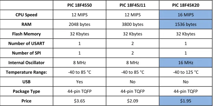
Consideration was taken into account of reusing the PIC 18F4550 microcontroller from the previous design or replacing it with a different microcontroller. The contending microcontroller choices were narrowed down to two families, the 18F K-series and J-series. Table 2 compares the possible microcontroller choices.
Table 2: Comparison of Microcontrollers
PIC 18F4550 PIC 18F45J11 PIC 18F45K20
CPU Speed 12 MIPS 12 MIPS 16 MIPS
RAM 2048 bytes 3800 bytes 1536 bytes
Flash Memory 32 Kbytes 32 Kbytes 32 Kbytes
Number of USART 1 2 1
Number of SPI 1 2 1
Internal Oscillator 8 MHz 8 MHz 16 MHz
Temperature Range: -40 to 85 °C -40 to 85 °C -40 to 125 °C
USB Yes No No
Package Type 44-pin TQFP 44-pin TQFP 44-pin TQFP
Price $3.65 $2.09 $1.95
The PIC 18F45J11 and 18F45K20 were considered because of their similarity in capabilities and characteristics with respect to the PIC 18F4550 used in UTOPIA 2.5. Two advantages that the PIC 18F45K20 has over the other choices are the faster CPU and higher internal oscillator speed which will improve performance. The PIC 18F45J11 does not improve on performance with respect to the existing microcontroller, but has more I/O capabilities because it features 2 UART and 2 SPI ports and allow more design possibilities. The advantage of reusing the PIC 18F4550 is that only slight changes to the PCB layout are required. However, the disadvantage is that the overall cost per device will be increased due to the proposed additional components such as the voltage regulator and FTDI USB-UART IC.
Option Selected and Justification
After evaluating all of the choices, It was determined that the best choice will be to replace the PIC 18F4550 with the PIC 18F45K20. All of the microcontroller options meet requirement 6 and 7 listed in Table 1, support of I/O capabilities and UART baud rate of 57 Kbaud, respectively. However, the
16
selection criterion was used to ultimately decide upon the microcontroller choice. The PIC 18F45K20 exceed many items in the selection criteria including lower unit cost, same 44-pin TQFP package type as in UTOPIA 2.5, higher CPU speed, and higher internal oscillator speeds. These items are highlighted in the shaded boxes of Table 2. The operating voltage range will support 3.3V and allow compatibility with the FTDI chip.
The features included in the PIC 18F4550 did not justify the higher cost since the USB is not a required feature. The dual SPI ports in the PIC 18F45J11 was determined to be unnecessary with clever design. The SPI port specifies three required signals, clock, data, and chip select. Although multiple SPI ports are required to interface the voltage controllers and ramping controllers, it is possible to parallel the clock and data signals with all the controllers and use a single digital output pin for each controller. Thus, each controller only operates when their chip select line is selected.
Voltage Regulator Component
The onboard voltage regulators regulate the amount of power applied to the hard drive. It provides independent control over the 5V and 12V rails. The purpose of adding this component to the UTOPIA board is to provide voltage margining from a single external power supply and allow power control in software.
Requirements and Selection Criteria
The input voltage for the power supply requires approximately 20 VDC with an operating range between 17 VDC and 24 VDC. The output voltages must be capable of supplying 18 VDC. Both rails must be independently controlled to allow maximum flexibility.
The selection criteria are listed as follows: provide the largest range of operating voltage for input and output, highest current output, and smallest PCB package type. The larger range in voltages provides more testing capabilities. The lowest output voltage value is desired.
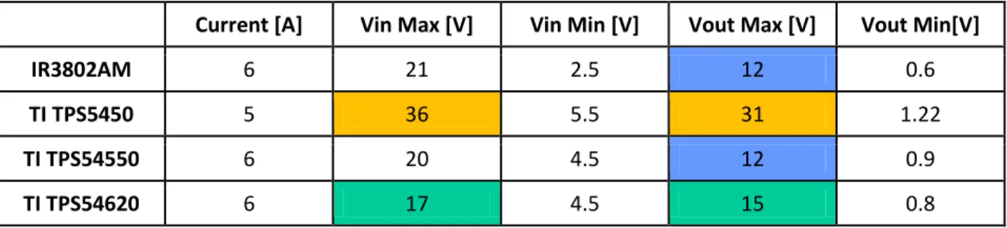
Options Considered
Below in Table 3, the technical specifications are compared between four DC/DC converters. Three out of the four choices are manufactured by Texas Instruments (TI) while the IR3802AM is made by International Rectifier (IR).
Table 3: Comparison of Switch Regulators
Current [A] Vin Max [V] Vin Min [V] Vout Max [V] Vout Min[V]
IR3802AM 6 21 2.5 12 0.6
TI TPS5450 5 36 5.5 31 1.22
TI TPS54550 6 20 4.5 12 0.9
17
These options were considered because of their ability to handle high currents. In the table, the minimum and maximum voltages for the input and output are specified. Different colors are used to distinguish each part’s ability to meet design requirements. The option with the highest maximum voltage for both input and output is the TPS5450 with up to 36 VDC for input and up to 31 VDC for output [3]. The option with the lowest maximum voltages is the TPS54550 with 20 VDC for input and 12 VDC for output [4]. The minimum values for the input voltage are negligible for all of the choices because the operating range is not expected to be below 17 VDC.
Option Selected and Justification
Two of the choices, IR3802AM and TPS54550, were immediately taken out of consideration as a result of not meeting the minimum voltage requirements in requirement 9 of Table 1. Only two options remain and the selection of the TI TPS5450 was due to its much larger operating voltage ranges. The TPS5450 meets requirement 8 and 9 in Table 1. Each rail will include its own individual DC/DC converter to meet requirement 10 of Table 1 which requires that each rail have support independent voltage margining.
Test Plan
Software testing will ensure that user commands perform the intended operation. For example, UTOPIA 2.5 features the power on command that should turn on the power outputs of the UTOPIA board. This function will be tested by using Hyperterminal to send the PON command to turn on the UTOPIA device’s power outputs. Then each rail on power output header will be measured by a digital multi-meter to determine whether the outputs are supplying power. Likewise, the POFF command should turn off the power outputs and measuring the power output header should read 0 VDC.
The data acquisition commands for measuring the voltages and currents will be tested to verify that the measurements are consistent with the actual value measured with a digital multi-meter. These tests involve sending the DATA command and a read out of the measurements are displayed in
Hyperterminal. Each rail of the power input header and power output header will be measured and errors of 0.1 VDC are acceptable.
The voltage margining feature in UTOPIA 3.0 will be tested by setting the power output voltage with the VSET5 and VSET12 command for the 5V rail and 12V rail, respectively. The command requires a voltage value in milli-volts. Once the voltage has been set, the output voltage is measured by a digital multi-meter and compared with the voltage setting. The measured values should be approximate to the voltage setting and calibration will be needed if the values do not match.
The testing for the OVP feature is very straight forward and only requires that the user not be allowed to set a voltage on the power output that is higher than the OVP value for the specified rail. The OVP value is predetermined and hardcoded into the firmware. The power outputs are measured by a digital multi-meter and it is required that the measured voltage value not exceed the OVP value.
18
IV. UTOPIA 3.0 IMPLEMENTATION
This chapter discusses the implementation of the four main circuit components: microcontroller, USB-UART IC, 5V and 12V regulator, and 5V and 12V switch. Then, the PCB layout and board fabrication will be covered. Lastly, the embedded firmware design will be described in detail.
Overview of CAD Software
The UTOPIA 3.0 prototype was designed using ExpressPCB CAD software. It includes two applications, one called ExpressSCH for drawing schematics and one called ExpressPCB for circuit board layout. The software creators provide circuit board manufacturing services. This method of prototyping is relatively low cost because the software is free and board manufacturing time takes approximately a week.
Circuit Schematic Design
There are four main circuit components that exist in UTOPIA 3.0 in which two of them are new additions to this design. The microcontroller and switch circuit already exist, while the USB-UART IC and voltage regulator circuit are new. The circuit schematics can be found in Appendix A. Each section will describe its interfaces and hardware functionalities.
Microcontroller
This component consists of the PIC 18F45K20 microcontroller, U1. The schematic can be found in Appendix A-1. It is interfaced to the USB-UART IC via UART using two signals identified as PIC TX and PIC RX. An SPI interface is used to communicate with the voltage ramping controllers, U2 and U3, and voltage regulator controllers, U15 and U16. The SPI interface requires three signals for each interface, SCLK, SDATA, and an individual chip select for each controller: SYNC_12, SYNC_5, PROG_5V, PROG_12V. The 5V rail requires two signals for control of its switch which are “5 PWM” and 5Control. Similarly, the 12V rail requires “12 PWM” and 12Control for control of its switch. The “Drive Vin” signal is used to measure input voltages and two signals, “+5vdr sense” and “+12 vdr sense”, measure voltage levels at the output. The signals that measure actual output voltages are 12VOLT and 5VOLT.
The ICSP header is used to flash firmware programs onto the microcontroller. An NTC1
thermistor is used to measure board temperatures. An external oscillator, X1, is used to provide it with a 20 MHz clock source. Future testing will determine whether the microcontroller’s internal oscillator is accurate enough so that this part can be removed. Two LEDs, D4 and D5, are connected for debugging purposes. Power is supplied to the chip via the 3.3V low-dropout (LDO) regulator.
USB-UART IC
The data sheet for the FTDI FT2232HL provides a recommended circuit example for the UART configuration. The circuit schematic can be found in Appendix A-6 in which the IC is labeled as U10. It has two UART interfaces in which port A is interfaced to the hard drive SIO port and port B is interfaced to the PIC microcontroller. Each interface only requires two signals, TX and RX. The USB interface requires two signals for data and is connected to the USB port.
19
A pairs of LEDs are connected to each port as status indicators for the TX and RX lines. The LEDs will blink when data is being transmitted. Additional components are required such as a 3.3V LDO regulator , U11, to provide a 3.3V operating supply, external EEPROM, U12, to store configuration settings, and external 12 MHz oscillator identified as X2.
5V/12V Voltage Regulator
Each voltage regulator circuit is essentially a TI TPS5450 DC/DC converter attached to a resistor divider network. The circuit schematic can be found in Appendix A-5 for the 5V regulator and Appendix A-4 for the 12V regulator. Note that each regulator is essential the same circuit, which is slightly modified from the recommended configuration provided in the TPS5450 data sheet [3]. Each rail is regulated by a single converter; the 5V rail is regulated by U14 and the 12V rail is regulated by U13.
The 12V rail is powered directly by the external power supply through the power input header. The voltage output is located on the output of the 15 μH power inductor, L3. The output voltages of the DC/DC converter can be adjusted by increments of 1/16 VDC depending on the equivalent resistance at the VSENSE port on pin 4 of U13. The ADG738, identified as U15, is a serially controlled 8-input MUX switch [5] and is responsible for generating the equivalent resistances. The MUX switch accepts an 8-bit binary value and turns on the inputs corresponding to the bit positions that are set high. The inputs, ranging between S1 to S8, conduct to ground and are then paralleled together to produce a parallel resistance value. With all switches in the “off” state or open, the TPS5450 defaults to output 2 VDC. Any combination of closed switches will add to the 2 VDC and result in an increase in output voltage. The total voltage output can reach a maximum of approximately 18 VDC. Each MUX switch is connected to a specific resistance value that is designed to provide the output voltages shown in Table 4. For example, if the MUX switch is set with the binary value “1000000” or 127 in decimal, the input at S8 will be switched on and the rest will be switched off. Thus, the total output voltage on the rail will be 10 VDC because of the default 2 VDC added to the 8 VDC supplied by the MUX switch.
Table 4: MUX Switch Settings
Switch Input S8 S7 S6 S5 S4 S3 S2 S1
Binary Bit Position 7 6 5 4 3 2 1 0
Output Voltage [V] 8 4 2 1 1/2 1/4 1/8 1/16
The 5V rail works in a similar fashion to the 12V rail. The only difference is that the resistors at the S7 and S8 inputs are not populated in the board fabrication. This limits the maximum total output voltage to approximately 6 VDC because the 8 VDC and 4 VDC outputs are not selectable.
5V/12V Switch
The switch circuit is referenced in Appendix A-2 and A-3. The 5V and 12V rails have nearly identical circuit configurations for the switch. The 12V switch will be described in detail and the characteristics can be applied to the 5V switch.
On the 12V switch, the 12Control signal turns on or off the power output in the 12V switch. The input voltages are passed into the source of a FET, U7, and forced through a feedback loop that is connected to the S1 input of the ADG738 MUX switch, U2. The output of the 12V switch is connected to pin 1 of the power output header, J5. Voltage ramping is controlled by a combination of PWM signals and a decade resistor network attached to the inputs of U2. The MUX switch provides a course method
20
of adjusting the ramping rate, while the “12 PWM” signal provides a fine tuning method. Depending on the MUX switch setting, the voltage ramps can be adjusted between 1 μs to 1s. The output of the MUX switch is connected to the positive input of a TL072 operation amplifier [6] identified as U6. The ADM4073F [7], identified as U4, is a voltage output, current-sense amplifier. It converts the current reading at the power output to an analog voltage value that can be used by the PIC microcontroller to measure the current of the 12V output in Amps. A LED, D2, is used to indicate the status of the switch output.
Similarly, the 5Control signal controls the output of the 5V switch. The input voltages are passed into the source of a FET, U9, and forced through a feedback loop that is connected to the S1 input of ADG738 MUX switch, U3. The output of the 5V switch is connected to pin 4 of the power output header, J5. Voltage ramping is controlled by a combination of PWM signals and a decade resistor network attached to the inputs of U3. The “12 PWM” is replaced with “5 PWM”. The output of the MUX switch is connected to the positive input of a TL072 operation amplifier identified as U8. The ADM4073F,
identified as U5, converts the current reading at the power output to an analog voltage value that can be used by the PIC microcontroller to measure the current of the 5V output in Amps. A LED, D3, is also used to indicate the status of the switch output.
PCB Layout Design
The board requires a relatively small footprint. The design utilizes a 4-layer PCB board which consists of a top, bottom, ground, and power layer. Components can be mounted on the top or bottom layer, while the power and ground layers are separately sandwiched in between. The board dimensions are approximately 2.5” x 2.5”. It is almost double the size of UTOPIA 2.5 which was 2” x 1.5”.
Overview of Design Procedures
The size of shape of each part is determined by its available package type in which some components only feature one specific one, while others have multiple types. Each part’s data sheet specifies this information along with recommended PCB patterns. Most of the parts such as resistors, capacitors, and ICs were standard and there were no issues finding it in the parts library of ExpressPCB. However, certain components such as the mini-USB plug and power inductors, L3 and L4, had PCB patterns that the parts library did not support. As a result, these parts had to be custom made by grouping together pads according to the measurements provided by their data sheets. For example, the power inductor specified a 12.8 mm x 12.8 mm square in which two 2.9 mm x 5.4 mm pads were separated by 7 mm. ExpressPCB provides a method of making the pads and using the built-in ruler to design a PCB pattern that met those specifications. Similarly, the mini-USB port was created by grouping traces and pads according to the specifications provided by the manufacturer’s data sheet.
Component placement was determined by the pin locations of each part. The strategy was to arrange each part so that traces lengths connecting two pins are minimized. All of the parts were first placed on the layout to determine the approximate board space required.
General PCB design rules were followed which includes running traces only horizontally, vertically, or at 45 degree angles [8]. The connections are routed with 7 mil traces that have a width of 0.007”. The power signals are routed with thicker 10 mil traces that have a width of 0.010”. A good
21
design practice is leaving at least a minimum gap of 7 mils surrounding traces. Filled planes are used to minimize current loss.
Top Layer
The PCB layout for the top layer is shown in Appendix B-2. It is subdivided into four parts in which the microcontroller is laid out on the top left section, the power output switches are laid out on the top right section, the voltage regulators are laid out on the lower right section, and the USB-UART IC is laid out on the lower left section.
Certain components had priority on the top layer. The large bulky components were placed on the top layer so that the board could lie flat on a lab bench surface. This included the aluminum capacitor, C16, which can be found in Appendix A-2 and C20 which can be found in Appendix A-3. The power inductors, L3 and L4, were also large components which are shown in Appendix A-4 and A-5, respectively. Also, the LEDs identified as D1, D2, D3, D4, D5, D8, D9, and D10 were placed on top so that they would be always visible.
Once all of the parts were laid out, it was a matter of orienting them such that placing the traces can be as short and direct as much as possible. For example, the FTDI USB-UART IC, U11, is oriented such that the traces for the TX and RX signals can be routed as short as possible to the PIC 18F45K20, U1. The output pins of the voltage regulators which are located on pin 2 of L3 and L4 are oriented to face the input of the power output switches. For L4, it is adjacent to C20 and is connected by a filled plane to minimize current loss. Likewise for L3, it is adjacent to C16 and provides the shortest path possible. Since there was no way to shorten the ground trace between the power input header and the power output header, a filled plane runs directly across the UTOPIA board to prevent current loss.
Bottom Layer
The bottom layer consists of the smaller or flat components such as resistors and the ADG738 MUX switches. Like the top layer, the board was subdivided into the sections mentioned in the previous top layer description above. The bottom layer is characterized by the long traces that run across the board. These are the clock, data, and chip select signals that connect between the microcontroller and the ADG738 MUX switches. In the lower right corner of the board, there is a filled plane that connects to the power input header and is spread out to reach the input terminals of the TI TPS5450 DC/DC
converters on top. Due to the lack of board space, it was difficult to connect the inputs. The solution was to use vias that connect between the top and bottom layers to make the connections. Again, the filled plane is used to minimize the loss of currents.
Board Fabrication
The manufacturing of the boards were made by ExpressPCB. Once the circuit schematic and PCB layout were complete, a final verification was done to verify that all of the connections were
implemented. The order is made online through the ExpressPCB software. The turnaround time for the boards took about a week from the date of the order. In order to reduce board costs, three copies of the layout were made onto a single PCB.
22
Upon visual inspection of the manufactured boards, two noteworthy errors were identified. A trace error caused by an unintentional short across capacitor C14 was found. This capacitor is part of the FTDI EEPROM circuit. It is an easy fix that only requires cutting the trace and should be corrected in the next board revision. The other error involved the PIC microcontroller and was caused by the routing an analog signal trace to a pin that was not assigned as an analog pin. Thus, it is not capable of reading the analog input. This will also be fixed in the next revision of the board, but for now, the incorrect pin and the correct pin will be shorted together to achieve correct functionality to develop the firmware.
While the boards were being manufactured, a parts order was placed at Digi-Key to obtain the remaining parts that were unavailable at Western Digital. In two weeks’ time, two complete Utopia boards were produced and ready for testing and development. It is important to note that there are some differences between the prototype and the circuit schematic due to unavailability of parts. Some of the resistor values on the voltage regulator components are not the exact values specified. The external oscillator on the prototype is rated at a frequency of 25 MHz and not the 20 MHz as specified in the schematic.
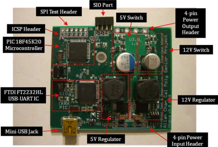
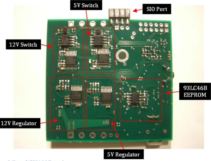
The two figures below highlights the location of the main board components on UTOPIA 3.0. Figure 4 shows the top of the board and each main component is identified by a dotted line. The I/O interfaces such as the mini-USB plug, power headers, and SIO port are also labeled. Figure 5 shows the bottom of the board and identifies the components placed below.
23
Figure 5: Photo of UTOPIA 3.0 (Bottom)
Software Architecture
This section describes the algorithm of the embedded system and the new commands that were implemented. The firmware for UTOPIA 3.0 is designed for the PIC microcontroller. The programming language is Basic. Code development was done using Proton Basic software [9 ].
24
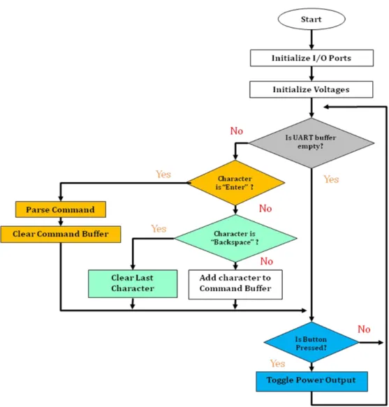
Software Algorithm
Figure 6: Software Flow Chart
The main loop algorithm is shown above in Figure 6. It is mainly used to parse commands from user input. It can be found in Appendix D on pages 49-50. Once the device has initialized its I/O ports and voltages, an infinite loop continuously checks the UART receive buffer for input from the user. If there is no data and the UART buffer is empty, then it checks whether the onboard button switch has been pressed. Pressing the button will toggle the power outputs and turn it on or off depending on the current state. If there is data in the UART buffer, each character is processed one at a time. Three conditions are checked: whether the input is an “Enter” key, a “backspace” key, or an alphanumerical key. The “enter” key indicates that the user is finished typing the command and the contents of the command buffer will be parsed to determine the action to perform. Once the command has been performed, the command buffer is cleared and ready to accept a new command. If the key press was a “backspace” key, then the previous character is removed from the command buffer. If the key is an alphanumerical character, then it is added to the command buffer.
25
Software Features
The software in UTOPIA 3.0 is responsible for three main tasks. It has to provide independent control of the power output switch, independent control of voltage margining, and perform data
acquisition of voltages and currents. The power output switch functionality and data acquisition features have already been implemented in UTOPIA 2.5. New software for voltage margining needs to be
developed to adjust the voltage settings and provide OVP on the power outputs.
The code for voltage margining is found in Appendix D between page 58-59. When the user calls the VSET5 or VSET12 command with a voltage value in millivolts, an if-statement checks whether the value is valid, either above the minimum voltage or below the OVP value. If it is valid, then it is converted to an 8-bit binary number for setting the MUX switch using the following formula:
SDATA = 256/16000 *(Vout – 2000)
Vout represents the value passed in from the VSET command. The value SDATA is a binary number ranging from 0-255 which is set on the MUX switch controlling the voltage rails.
The OVP feature was suggested during firmware development. The user can change the OVP for each rail independently or query for the OVP value. Its implementation is simple and only requires adding two registers to store the value in memory. The code can be found in Appendix D on page 53. On page 48, the registers are initialized with the values MAXOVP5 and MAXOVP12 which are the default OVP values on each rail. The user calls the command OVP5 or OVP12 with a voltage value in millivolts. An if-statement determines whether the value is valid and sets the new OVP value if it is. The valid voltage range for the 5V rail is 3 VDC to 6 VDC and for the 12V rail is 3 VDC to 18 VDC.
Existing Commands
The commands listed below in Table 5 are already implemented in UTOPIA 2.5. The PON and POFF commands are used to power on or power off the power outputs, respectively. Independent switching is also available for each power output using the PON5, POFF5, PON12, and POFF12 commands. The remaining commands in the list are used to take measurements of input voltages, output voltages, output currents, and board temperature.
Table 5: Existing UTOPIA 2.5 Commands
Output Switch
PON
Turns on 5V and 12V outputs
POFF
Turns off 5V and 12V outputs
PON5
Turns on 5V output
POFF5
Turns off 5V output
PON12
Turns on 12V output
POFF12
Turns off 12V output
26
Status
TEMP
Displays board temperature
DATA
Displays voltage and current measurements
CUR
Displays current measurements
VOLTS
Displays voltage measurements
U3ID
Displays the firmware version
New Commands
In addition to the existing commands, there are seven new commands for UTOPIA 3.0 listed in Table 6 that has been developed to control the voltage regulators. One pair of commands, VSET5 and VSET12, adjusts the voltage settings on the power outputs. Four commands are related to the over-voltage-protection (OVP) feature. The commands, OVP5 and OVP12, set the maximum voltage possible on the power output. The commands, GETOVP5 and GETOVP12, read back the OVP value on the 5V rail and 12V rail, respectively.
Table 6: New UTOPIA 3.0 Commands Power Settings
VSET5 volts Sets the voltage value on the 5V rail in mV VSET12 volts Sets the voltage value on the 12V rail in mV
OVP Settings
OVP5 volts Sets the over-voltage-protection value on the 5V rail in mV OVP12 volts Sets the over-voltage-protection value on the 12V rail in mV
OVP Status
GETOVP5 Reads back the over-voltage-protection value on the 5V rail GETOVP12 Reads back the over-voltage-protection value on the 12V rail
Miscellaneous
27
V. INTEGRATION AND TEST
Chapter 5 describes the testing that was involved for the UTOPIA 3.0 device. Testing verified that the design is sound and meets requirements. The results are presented and recommendations for the next board design conclude the chapter.
Acceptance Testing
The final prototype is expected to meet the requirements listed in Table 1. Each component of the board must be tested to ensure successful operation upon integration. Specifically, the UTOPIA device was tested on accepting commands, supplying power to hard drive, and communicating with SIO port.
The UTOPIA 3.0 device’s ability to accept commands was tested first. Only the commands related to setting the voltage, controlling the power outputs, and data acquisition were tested. For each tested voltage setting, the power outputs were measured and recorded. It was deemed a success as long as the voltage measurement was within 1 VDC difference because the hardware has not been calibrated. The power outputs were tested by issuing the commands and making sure that the power on command applied power to the output terminals and the power off command removes power from the output terminal. The voltage measurements in software were compared to measurements by electronic measuring tools. The current measurements and board temperature were not included in the final testing. It will be performed in the next stage of development where precision tools will be available.
The ability to supply power to the hard drive was tested next. The main task was to make sure voltage margining was functional and the power outputs could be switched on and off. Initially, the voltages were set by sending a value between 0 and 255 via SPI protocols to the ADG738 MUX switches which it uses to adjust the voltage setting. Different values switch on different combinations of the 8 input switches and, in turn, provide different voltage outputs.
Communication with the SIO port was tested at Western Digital and involves running SASDEX, test script software, to run an automated test script that repeatedly powers up and down the hard drive at two different pairs of voltage settings. The test results have been shown that it meets Western Digital specifications.
Test Report
The tests included in this report demonstrate basic operation of UTOPIA 3.0. The voltage ramping features was not tested at this time because it was beyond the scope of the project. There are five tests and they aim to verify basic functionality of UTOPIA 3.0.
28 Test: Program PIC microntroller
Description: This test flashes a blinking LED program onto the PIC microntroller. It demonstrates that the microcontroller can be flashed with a program. The two debugging LEDs are set to alternately blink continuously at a rate of 100 ms.
Equipment: UTOPIA 3.0 device, PICkit 2 Programmer, mini-USB cable, PICkit 2 v2.61 programming software
Procedure: 1. Connect PICkit 2 to PC using mini-USB cable 2. Connect PICkit 2 to ICSP header
3. Import HEX file into PICkit 2 software and click "Write" button
4. PIC microcontroller will perform a power-on reset and begin running the program Results: The blinking LED program loaded successfully. After the reflash, the PIC microcontroller
performs a reset and the LEDs start blinking in the middle of the board.
Test: SPI Test Header
Description: The SPI test header provides an external connection for communication via SPI 3-wire protocols. It supports input and output of data. This test demonstrates that the PIC microcontroller sends valid data to the ADG739 MUX switches for voltage margining and ramping control
Equipment: UTOPIA 3.0 device, Oscilloscope, 3 scope probes, Hyperterminal, mini-USB cable Procedure: 1. Connect UTOPIA 3.0 device to mini-USB cable
2. Attach 1 scope probe to pin 2 of SPI test header to measure SCLK 3. Attach 1 scope probe to pin 4 of SPI test header to measure SDATA
4.Attach 1 scope probe to pin 5 of SPI test header to measure SPI head CS (chip select) 5. Set Oscilloscope to trigger on SPI head CS on falling edge
6. Open Hyperterminal and type in "SPI5 10" 7. Read output from oscilloscope
Results: The oscilloscope measures all three signals, SCLK, SDATA, SPI head CS. The port is activated by the SPI head CS signal when it selects low and data transmission stops when the chip select turns off and idles high. Data transmission occurs in 8-bit words and is transferred bit by bit on each clock cycle. Output is expected to show the chip select toggled low and a binary sequence of the value 10 that is timed to the clock signal. The binary equivalent of '10' (0b00001010) is shown on the scope in addition to a toggling clock source. The results meet expectation.
29 Test: Software OVP
Description: Provides a over-voltage-protection limit on the UTOPIA 3.0 power outputs. This test makes sure that voltages cannot be set higher than the default OVP settings, 5.3 VDC on the 5V rail and 13.3 VDC on the 12V rail.
Equipment: UTOPIA 3.0 device, mini-USB cable, External 20 VDC power supply, digital multi-meter Procedure: 1. Connect UTOPIA 3.0 device to PC using mini-USB cable
2. Connect digital multi-meter to 5V power output
3. Connect power supply to UTOPIA 3.0 power input header 4. Open Hyperterminal and connect to UTOPIA 3.0 device 5. Call "VSET5 6000" command to set 6 VDC on 5V rail 6. Call "VSET12 15000" to set 15 VDC on 12V rail 7. Measure voltages at power output header
Results: The test sets the power outputs to settings that exceed the OVP value. The results meet expectations. In both situation, the power outputs are unchanged and an error message notifies the user that the voltage setting was too high.
Test: Power Output Switch
Description: This test is performed to ensure that the power on command switches on the power output and the power off command switches off the power output.
Equipment: UTOPIA 3.0 device, mini-USB cable, External 20 VDC power supply, digital multi-meter Procedure: 1. Connect UTOPIA 3.0 device to PC using mini-USB cable
2. Connect power supply to UTOPIA 3.0 power input header 3. Open Hyperterminal and connect to UTOPIA 3.0 device 4. Call "VSET5 6000" command to set 6 VDC on 5V rail
5. Connect digital multi-meter to 5V power output and measure voltages at power output header
6. Call "VSET12 15000" to set 15 VDC on 12V rail
7. Connect digital multi-meter to 12V power output and measure voltages at power output header
Results: The test sets the power outputs to settings that exceed the OVP value. The results meet expectations. In both situation, the power outputs are unchanged and an error message notifies the user that the voltage setting was too high
30 Test: Voltage Margining
Description: Ensure that voltage margining is functional on the 5V rail and 12V rail. A range of voltage settings are selected and set on the UTOPIA 3.0 device. The power outputs are measured and compared to the voltage settings
Equipment: UTOPIA 3.0 device, mini-USB cable, External 20 VDC power supply, digital multi-meter Procedure: 1. Connect UTOPIA 3.0 device to PC using mini-USB cable
2. Connect power supply to UTOPIA 3.0 power input header 3. Open Hyperterminal and connect to UTOPIA 3.0 device 4. Call "VSET5 5000" command to set 5 VDC on 5V rail
5. Connect digital multi-meter to 5V power output and measure voltages 6. Call "VSET12 12000" to set 12 VDC on 12V rail
7. Connect digital multi-meter to 12V power output and measure voltages 8. Repeat steps 4 through 7 for each voltage setting desired for testing
Results: The voltage settings and measured voltages are compared in the tables below. Table 7 lists the measurements for the 12V rail. The values are very closely matched to the voltage setting and have less than 1% error approximately. In Table 8, the 5V rail has slightly more percent error with up to almost 2% error. The amount of error for both outputs is acceptable because the certain resistance values for the decade resistor network in each voltage regulator don’t all match exactly to the circuit schematic.
Table 7: 12V Rail Power Output Measurements
12V Rail Measurements
Setting [V] Measured Voltage [V] Percent Error [%]
3.00 2.99 0.3 5.00 4.97 0.6 11.50 11.42 0.7 12.00 11.93 0.6 12.50 12.42 0.7 13.30 13.16 1.1
Table 8: 5V Rail Power Output Measurements
5V Rail Measurements
Setting [V] Measured Voltage [V] Percent Error [%]
3.00 2.98 0.7 4.00 3.96 0.9 4.50 4.44 1.3 5.00 4.95 1.1 5.10 5.01 1.8
31
Results
Successes
The PCB board has a relatively low number of defects due to design. The problems were not severe and fixed with temporary solutions that did not hinder our ability to make progress on board development. There have been no known defects due to manufacturing, so it appears that all of the spacing and trace widths are acceptable. All of the parts have been tested for correct functionality and compatibility. The goal of the project has been reached with the PC able to communicate with the Utopia board and control the voltages. This board is now able to be used as a base for further
development such as calibrating the voltage outputs to be more accurate, testing higher data transfer rates, and determining the potential of the powerful microcontroller.
Shortcomings
There have been no major failures so far that prevent the UTOPIA device from functioning normally. However, an issue with the Hyperterminal interface has not been resolved. The initial
character of the very first typed command is always corrupted due to an apparent hardware issue. That is, the first character does not match the character typed on the keyboard on startup. The issue is resolved by deleting this character and it never occurs again until the next restart. This issue will require more debugging and testing to determine a solution.
Design Recommendations
1. One of the capacitors (C14) connected to the FTDI IC chip contain an electrical short across its pins. This can be fixed by removing the electrical short.
2. Resistors R3, R4, R13, and R14 should have resistance values of 1 Kohm rather than 249 ohm. The resistors placed on the board are actually 1 Kohm and the change only needs to be made to the circuit schematic.
3. There is an analog signal trace that is routed to a wrong pin on the PIC microcontroller. The analog pin for the 5CUR signal should be connected to pin 22 and not pin 23. This was due to an error in the circuit schematic that connected the analog signal to a pin that does not support analog measurements.
32
VI. FURTHER DEVELEPMENT/TESTING
There are three items that need to be addressed in future development before UTOPIA 3.0 is ready for mass production.
One of the items is to determine whether the EEPROM for the FTDI USB-UART IC should be included for all boards. The EEPROM is not required for proper device operation. However, it is not possible to adjust the brightness of the TX and RX status LEDs without it. The advantages and disadvantages will need to be taken into consideration before a decision can be made.
Secondly, the PIC 18F45K20’s built-in internal oscillator which is capable of clock speeds up to 64 MHz will need to be thoroughly tested for accuracy at clock speeds higher than 20 MHz. It is unknown whether it is advantageous to run at a higher speed, so the UTOPIA 3.0 prototype will be evaluated at different speeds.
It is also important to calibrate the analog readings of the voltages and currents from the power input and output in order to provide accurate measurements in software. Precise testing equipment will be used to measure the actual values and the software will be tuned to match the analog readings to the actual measurements.
33
VII. BIBLIOGRAPHY
[1] Microchip. "PIC 18F2455/2550/4455/4550 Data Sheet." 27 October 2009. Microchip.com. 14 November 2009 <http://ww1.microchip.com/downloads/en/DeviceDoc/39632e.pdf>. [2] FTDI Ltd. "FT2232H Datasheet v2.06." 21 September 2009. ftdichip.com. 21 January 2010
<http://www.ftdichip.com/Documents/DataSheets/DS_FT2232H_V206.pdf>.
[3] Texas Instruments. "TPS5450EVM-254 5-A, Swift Regulator Evaluation Module." 9 March 2007. focus.ti.com. 10 December 2009 <http://www.ti.com/litv/pdf/slvu211>.
[4] Texas Instruments. "TPS54550EVM-158 Swift Regulator EVM." 29 March 2006. focus.ti.com. 13 November 2009 <http://www.ti.com/litv/pdf/slvu151>.
[5] Analog Devices. "ADG738: CMOS, Low Voltage, Single 8 to 1 Multiplexer, Serially Controlled Matrix Switch." May 2000. analog.com. 8 March 2010
<http://www.analog.com/static/imported-files/data_sheets/ADG738_739.pdf>.
[6] Texas Instruments. "TL072 Dual Low-Noise JFET-Input Gen. Purpose Operational Amplifier." 23 March 2005. focus.ti.com. 10 March 2010 <http://www.ti.com/lit/gpn/tl072>.
[7] Analog Devices. "ADM4073: LOW COST, VOLTAGE OUTPUT, HIGH-SIDE CURRENT SENSE
AMPLIFIER." October 2006. analog.com. 16 March 2010 <http://www.analog.com/static/imported-files/data_sheets/ADM4073.pdf>.
[8] ExpressPCB. "Tips for Designing PCBs." expresspcb.com. 10 December 2009 <http://www.expresspcb.com/ExpressPCBHtm/Tips.htm>.
34
APPENDIX A: Circuit Schematics
35
Appendix A-2: 12V Switch
36
Appendix A-3: 5V Switch
37
Appendix A-4: 12V Regulator
38
Appendix A-5: 5V Regulator
39
Appendix A-6: USB-UART IC
40
APPENDIX B: PCB Layout Design
41
Appendix B-2: Top Layer
42
Appendix B-3: Bottom Layer
43
APPENDIX C: Bill of Materials
PIC Microcontroller (18F45K20)
Count Part
ID Value Description Size MFR Part Number MFR
Digi-Key Part Number Unit Price 2 C10, C11 20pf Capacitor 0603 WD part 0.005
1 D4 Blue Discrete LED 0603 APG1608QBC/E Kingbright
754-1352-1-ND 0.72
1 D5 White Discrete LED 0603 WD part 0.195
2 R1, R50 10K Resistor 0603 WD part 0.005 1 R42, R43 220 Resistor 0603 WD part 0.005 1 R45 100K Resistor 0603 WD part 0.005 1 NTC1 10K Resistor 0603 WD part 0.005 1 X1 25 MHz Crystal 5.0mm x 3.2mm NX5032GA-25.000000MHZ NDK 644-1041-1-ND 0.81 1 U1 18F45 K20
IC PIC MCU FLASH
16KX16 44-TQFP 44-TQFP PIC18F45K20-E/PT Microchip PIC18F45K2 0-E/PT-ND 3.1 Total 4.86 USB-UART IC (FTDI FT2232HL) Count Part
ID Value Description Size
MFR Part Number MFR Digi-Key Part Number Unit Price 2 C1, C3 4.7uF Polarized Capacitor 0603 WD part 0.005 2 C15, C17 18pF Capacitor 0603 WD part 0.005 12 C4, C5, C9, C12, C14, C18, C19, C21, C22, C23, C29, C26 C9, C12
.1uF Capacitor 0603 WD part 0.005
44 Count Part
ID Value Description Size
MFR Part Number MFR Digi-Key Part Number Unit Price
1 C13 3.3uF Capacitor WD part 0.005
1 R2 1K Resistor 0603 WD part 0.005 1 R41 12K Resistor 0603 WD part 0.005 3 R44, R51, R52 10K Resistor 0603 WD part 0.005 1 R53 2.2K Resistor 0603 WD part 0.005 4 R56, R57, R58, R59 220 Resistor 0603 WD part 0.005 1 X2 12Mhz Crystal 5.0mm x 3.2mm ABM3-12.000MH Z-B2-T Abracon Corporation 535-9100-1-ND 1.88 2 D1, D9 Green Discrete LED 0603 Kingbright Corp
754-1356-2-ND 0.195 2 D8,
D10 Red Discrete LED 0603 Avago Technologies
516-2005-1-ND 0.5 1 U10 FT223 2H FTDI USB-UART IC 64-LQFP FT2232HL - REEL FTDI, Future Technology Devices International Ltd 768-1024-1-ND 6.71 1 U11 MCP1 700T
CMOS low dropout (LDO) Voltage Regulator, 3.3V SOT-23 3-pin MCP1700 T-3302E/TT Microchip MCP1700 T3302ETT CT-ND 0.45 1 U12 93LC4 6B 1Kbit low-voltage serial Electrically Erasable PROMs (EEPROM) SOIC - 0.050 pitch - 8 pin 93LC46B-I/SN Microchip 93LC46B-I/SN-ND 0.34 Total 10.91 5V and 12V Regulator
Count Part ID Value Description Size MFR Part
Number MFR Digi-Key Part Number Unit Price 6 C31, C32, C33, C42, C43, C44
.01uF Capacitor 0603 WD part 0.005
2 C40, C45 .1uF Capacitor 0603 WD part 0.005
2 C30, C41 10uF Capacitor 1812 C4532Y5V1H
106Z TDK 445-3483-1-ND 3.02 2 D11, D12 B540 C Diode DO-214AB, SMC B540C-13-F Diodes Inc B540C-FDICT-ND 1.08 2 R64, R78 2.5K Resistor 0402 WD part 0.002 1 R73 3K Resistor 0603 WD part 0.005 2 R65, R79 5K Resistor 0402 WD part 0.002 2 R66, R88 10K Resistor 0402 WD part 0.002
45
Count Part ID Value Description Size MFR Part
Number MFR Digi-Key Part Number Unit Price 2 R67, R81 20K Resistor 0402 WD part 0.002 2 R60, R74 31.6K Resistor 0402 WD part 0.002 1 R72 33K Resistor 0603 WD part 0.005 2 R61, R75 34.0K Resistor 0402 WD part 0.002 2 R62, R76 36.5K Resistor 0402 WD part 0.002 2 R68, R82 40K Resistor 0402 WD part 0.002 2 R69, R83 80K Resistor 0402 WD part 0.002 2 R63, R77 86.6K Resistor 0402 WD part 0.002 2 R70, R84 160K Resistor 0402 WD part 0.002 2 R71, R85 320K Resistor 0402 WD part 0.002 2 L3, L4 15uH Power Inductor 12.8mm x 12.8mm CDRH127/LD NP-150MC SUMIDA AMERICA COMPONENTS INC 308-1333-1-ND 2 U15, U16 ADG7
38 IC MUX 16-TSSOP ADG738BRU Z Analog Devices ADG738BR UZ-ND 3.85 2 U13, U14 TPS5 450 TPS5450 Step Down Conv 8-SOIC Exposed Pad TPS5450DDA R Texas Instruments 296-21715-5-ND 6.25 Total 28.5 5V and 12V Switch
Count Part ID Value Description Size MFR Part
Number MFR Digi-Key Part Number Unit Price 10 C2, C7, C8, C25, C27, C28, C29, C34, C35, C38
.1uf Capacitor 0603 WD part 0.005
1 C16 150uF25 vPoly Aluminum Capacitor 0.327" L x 0.327" W EMVE250A DA151MHA 0G United Chemi-Con 565-2221-1-ND 0.85 1 C20 470uF10 vPoly Aluminum Capacitor 0.406" L x 0.406" W PCF1A471M CL1GS Nichicon 493-2996-1-ND 1.99 4 C6, C24, C36, C37 .001uF WD part 0.005 2 D2, D3 Red Discrete LED 0603 Avago Technolog ies 516-2005-1-ND 0.5 2 D6, D7 Schottky WD part 0.005 2 R33, R34 0.02
Ohm Resistor 0603 WD part 0.005
2 R5, R15 20 Ohm Resistor 0603 WD part 0.005
2 R27, R30 50 Ohm Resistor 0603 WD part 0.005
2 R6, R16 200
Ohm Resistor 0603 WD part 0.005