ELECTROMECHANICAL RESPONSE OF
TEXTURED FERROELECTRIC PZT THIN FILM STACKS
BY
DEBASHISH DAS
DISSERTATION
Submitted in partial fulfillment of the requirements
for the degree of Doctor of Philosophy in Aerospace Engineering in the Graduate College of the
University of Illinois at Urbana-Champaign, 2017
Urbana, Illinois
Doctoral Committee:
Professor Ioannis Chasiotis, Chair and Director of Research Professor John Lambros
Professor Nancy R. Sottos Professor Philippe H. Geubelle
ii
ABSTRACT
Thin film piezoelectric materials with high piezoelectric coefficients such as PbZr0.52Ti0.48O3 (PZT) offer several advantages to microelectromechanical systems (MEMS) due to their low power requirements, large displacements, high work and power densities, as well as high sensitivity in a wide dynamic range. The performance of PZT-based MEMS can be further improved by increasing the piezoelectric response of PZT polycrystals via texture control. However, freestanding PZT films, in particular for MEMS, are comprised of several other films forming a stack. These additional layers serve as seeding (TiO2), buffer (SiO2), and conducting (Pt) layers with substantial thickness and stiffness compared to the main PZT layer. As a result, quantitative understanding of the mechanical behavior of each layer is required in order to extract the electromechanical response of the PZT layer itself in a stack.
This dissertation research investigated (a) the mechanical behavior of highly {111} textured Pt films grown on {100}-TiO2 which is required to achieve ~100% (001)-textured PZT films, and (b) the electromechanical behavior of freestanding (001)-textured PZT film stacks, with PZT texture varying from 100% (001) to 100% (111). PZT stacks in the form of d31-type actuators were comprised of an elastic SiO2 layer, an adhesion layer of
{100}-textured rutile TiO2, a metallization layer of highly {111}-textured Pt, a seed layer of PbTiO3, the PZT layer, a second Pt metallization layer, and, finally, a thin ALD layer of Al2O3 and HfO2 deposited by atomic layer deposition.
Microscale uniaxial tension tests were carried out on patterned SiO2 films and combinations of layers, such as TiO2-Pt, TiO2-Pt, TiO2-Pt-PZT and SiO2-TiO2-Pt-PZT-Pt-ALD to determine the properties of each layer. Experiments on TiO2-Pt stacks with different Pt thickness showed that a reduction in film thickness increases the flow stress of Pt. The evolution of flow stress with plastic strain as a function of film thickness and grain size was successfully modeled, providing insight into the deformation behavior of polycrystalline metal films grown epitaxially on polycrystalline underlayers. Mechanical experiments on (SiO2-TiO2-Pt-PZT) and full PZT stacks (SiO2-TiO2-Pt-PZT-Pt-ALD) showed that the mechanical, piezoelectric and ferroelastic properties of PZT
iii
thin films depend strongly on grain orientation. The open circuit PZT modulus varied linearly with %(001) and %(111) texture factors between the two texture bounds: a lower bound for 100% (001) and an upper bound for 100% (111). Pure (001) texture exhibited maximum non-linearity and ferroelastic domain switching, contrary to pure (111) texture with more linear behavior and the least amount of switching. A micromechanics model based on the Eshelby inclusion problem was employed to calculate the strain due to domain switching. The model reproduced the experimentally observed non-linearities in the stress vs. strain curves of (001) and (111) textured PZT films. Finally, the linear piezoelectric and ferroelectric properties of textured PZT films at low and high electric fields, respectively, were calculated using laser Doppler vibrometer measurements on PZT unimorphs. All samples, except one comprised of 73% (001) and 27% (111) texture, demonstrated saturation in transverse piezoelectric coefficients beyond ~150 kV/cm. Notably, the sample with the combination of 73% (001) and 27% (111) textures showed stable transverse piezoelectric coefficients at all electric field values with technologically significant implications to ultra-low-power MEMS. The ferroelectric and linear piezoelectric coefficients (with the exception of the aforementioned sample with stable linear properties) depended strongly on film texture, and the effective transverse strain and stress coefficients varied linearly with %(001) and %(111) texture factors. PZT films with 100% (001) orientation displayed 150%, 140%, and 80% larger linear piezoelectric strain coefficient, saturated strain coefficient and saturated stress coefficient, respectively, compared to films with 100% (111) orientation for the same electric bias and the same film thickness. Finally, PZT films with pure (001) texture showed 20% higher dielectric constant and 50% higher figure of merit in sensing than films with pure (111) texture.
This dissertation research provided insight into material microstructure-electromechanical property relationships for freestanding PZT film stacks. The results will assist the development of reliable low power PZT-based MEMS devices with higher actuation and better sensing characteristics.
iv
ACKNOWLEDGEMENTS
I am grateful to my advisor, Prof. Ioannis Chasiotis, for his constant support and guidance which not only proved invaluable for the successful completion of this dissertation but also helped me develop the skill-sets in the field of nanomechanics which was initially a steep learning curve for me being from a material science background. He showed extreme patience and helped me through tough times during the completion of this dissertation research. I would also like to acknowledge the ARO grant # W911NF-12-1-0204 for supporting my research.
I would like to extend my sincere gratitude to our collaborators, Dr. Ronald Polcawich of Army Research Laboratory (ARL), Adelphi, MD for providing me the samples, providing insightful discussions and suggestions and help me carry out experiments at ARL. I am also indebted to Dr. Ryan Rudy of ARL for showing me the facilities at ARL and helping me carry out the electrical characterization of the PZT films at ARL. I will like to thank Prof. Sottos, Prof. Lambros, and Prof. Geubelle for agreeing to serve on my doctoral committee and providing invaluable feedback during my preliminary examination that was crucial to improving this dissertation.
Many thanks are due to all my present and past lab mates from Prof. Chasiotis’s research group, especially Mr. Korhan Sahin, Dr. Pavan Kolluru, Dr. Sivakumar Yagnamurthy, Dr. Nikhil Karanjgaokar, Mr. Dimitrios Antartis and Mr. Fan Yang for their invaluable discussions which have always helped bring in a fresh perspective to the problems at hand.
I would like to sincerely thank the Aerospace Department staff for their constant support, especially the machine shop members Mr. Greg Milner and Mr. Lee Booher for their valuable suggestions to improve the design of parts, and to Ms. Staci McDannel and Ms. Kendra Lindsey for help with administrative issues. I also extend my thanks to the staff at Material Research Laboratory for training me on several necessary instruments, primarily to Dr. Jim Mabon for FIB and SEM training, Dr. Mauro Sardela for XRD training, and Dr. Scott Maclaren for AFM training.
v
I am forever grateful to my parents, my wife, Pikee Priya and my relatives for the constant encouragement, support and for believing in me. Finally, I would like to thank my friends Esperanto, Chaitanya, Shamiparna, Alok, Avinash, Anand and many others for supporting and being there for me.
vi
TABLE OF CONTENTS
Chapter 1: Introduction ... 1
1.1 Motivation and Approach ... 2
1.2 Structure and Recent Advances in Fabrication of PZT Films ... 8
1.3 Mechanical Behavior of Textured Thin Films ... 12
1.4 Research Objectives and Approach ... 14
1.4.1 Research Methods and Tasks ... 17
1.5 Outline of this Dissertation ... 17
Chapter 2: Experimental Methods ... 19
2.1 Experimental Methods for Mechanical Testing of Thin Films ... 19
2.2 Microscale Tension Experiments with Thin Films ... 21
2.3 Ferroelectric Characterization of Thin Film PZT Stacks ... 27
2.3.1 Measurement of Ferroelectric and Dielectric Properties ... 29
2.4 Summary ... 31
Chapter 3: Mechanical Behavior of Epitaxially Grown {111} Textured Pt Films ... 32
3.1 Experimental Methods ... 35
3.1.1 Specimen Preparation and Materials Characterization ... 35
3.2 Elastic Properties of Pt and TiO2 Films ... 43
3.3 Inelastic Response of Pt Films ... 46
3.3.1 Model for Initiation of Plastic Deformation ... 49
3.3.2 Dislocation Nucleation at Film Surface due to Surface Roughness ... 57
3.3.3 Prediction of Plastic Flow Stress ... 59
3.4 Strain Rate Sensitivity of Pt/TiO2 Films ... 62
3.5 Conclusions ... 67
Chapter 4: Mechanical Response of Textured PZT Films ... 68
4.1 Experimental Methods ... 72
4.2 Stress-strain Response of Textured PZT Films ... 76
vii
4.4 Elastic Modulus as a Function of Texture... 86
4.5 Conclusions ... 88
Chapter 5: Control of Ferroelectric Response of PZT Films through Texture ... 89
5.1 Experimental Methods ... 90
5.1.1 Specimen Preparation and Materials Characterization ... 90
5.1.2 Measurement of out-of-plane Displacement and Piezoelectric Properties .. 92
5.2 Results and Discussion ... 92
5.2.1 Unipolar Piezoelectric Actuation ... 92
5.2.2 High Field Effective Transverse Piezoelectric Coefficients ... 94
5.2.3 Low Field Effective Transverse Piezoelectric Coefficients ... 105
5.2.4 P-E Hysteresis Loops and Bipolar Piezoelectric Actuation ... 110
5.3 Conclusions ... 114
Chapter 6: Conclusions… ... 115
6.1 Assessment of Dissertation Outcomes ... 115
6.1.1 Mechanical Response of Epitaxially Grown {111} Pt Thin Films ... 116
6.1.2 Effect of Texture on Mechanical Response of PZT Thin Films ... 117
6.1.3 Effect of Texture on the Ferroelectric Response of PZT Thin Films ... 118
6.2 Future Directions ... 119
1
CHAPTER 1
Introduction
Microelectromechanical systems (MEMS) integrate miniaturized elements with combined mechanical and electrical functionalities via microfabrication techniques that produce typical feature sizes in the 1-100 µm range. The field of MEMS has grown significantly with the advent of modern electronics and recent advances in fabrication technologies by which both sensing and actuation elements could be realized on-chip. Motion in MEMS can be generated by different means, such as thermal, electrostatic, magnetostrictive, and piezoelectric. However, most current MEMS devices are actuated electrostatically which requires significant actuation voltage that necessitates large external sources. The alternative piezoelectric actuation, particularly based on lead zirconate titanate (PZT) films, offers several benefits, such as the unique combination of high work and power densities, superior power efficiency, and low voltage actuation. PZT thin film actuators with very high piezoelectric coefficients can achieve significant forces and structural displacements at small voltages, thus eliminating the need for bulky power conditioning circuits. PZT sensors, on the other hand, do not require external energy sources, offering the possibility of ultra-low-power miniaturized systems. PZT transduction has also been utilized for energy harvesting [1]. Other examples of PZT-MEMS devices include radio frequency (RF) switches [2], ultra-low power mechanical logic [3], inkjet printer heads [4], biosensors [5] and millimeter scale robotics [6].The performance of PZT-MEMS devices hinges upon the piezoelectric response of the PZT films that is quantified by the piezoelectric coefficients. Epitaxial and strong-oriented piezoelectric films with a well-defined polar axis orientation may further increase the actuation force produced by PZT-based MEMS. The electromechanical
2
properties of PZT thin films depend on the fabrication process [7] and, thus, differ significantly from bulk PZT. The key differentiating factor of freestanding PZT thin films fabricated for MEMS devices is the significant thickness of all auxiliary films acting as electrodes or support relative to the thickness of the PZT film itself, which affects the maximum output displacement. Furthermore, epitaxial PZT films grown on silicon substrates need suitable seed and buffer layers that act as structural templates and barriers against Pb cation migration into Si. Epitaxial PZT films are usually deposited thinner than randomly oriented films since the thinner textured/epitaxial films require lower coercive voltages while displaying comparable remnant polarizations. Because of their multilayer structure, PZT films fabricated for MEMS are henceforth referred to as PZT stacks. The grain structure and texture of underlying films in a PZT stack bias and control the texture of the PZT layer itself, requiring mechanical characterization of each layer in the stack to ensure the mechanical performance and reliability of PZT-MEMS.
1.1 Motivation and Approach
Epitaxial films may be deposited with several different textures and their combinations which directly influences their piezoelectric and mechanical properties. A large number of possible textures and the difficulty in preparing and testing PZT films with different texture have limited the number of available comprehensive studies [8-14]. Even more scarce are data on freestanding PZT films. Prior studies of PZT films using uniaxial tension [15], nanoindentation [8-10], membrane deflection techniques [16,17] and resonance frequency techniques [11] have reported a broad range of values for the elastic modulus, ranging between 37 GPa [18] and 400 GPa [19]. The lack of a large and consistent base of experimental modulus data has implications in the calculation of other important properties of PZT films. For instance, determination of the piezoelectric strain coefficient, d31*, requires explicit knowledge of the elastic modulus [20-22]. Inaccuracies
* Piezoelectric strain coefficient (𝑑𝑖𝑗𝑘) is the linear coupling factor between polarization (𝑃𝑖) and applied stress (𝜎𝑖𝑗) for the direct piezoelectric effect, 𝑃𝑖= 𝑑𝑖𝑗𝑘𝜎𝑗𝑘. Alternately, it is the linear coupling factor between strain (𝜀𝑖𝑗) and electric field (𝐸𝑖) for the converse piezoelectric effect, 𝜀𝑖𝑗 = 𝑑𝑘𝑖𝑗𝐸𝑘.
3
in the values of the latter could be responsible for the vast disparities in the values of d31
reported in the literature, in the range of 30 pmV-1 [23] to 180 pmV-1 [24]. Furthermore, existing literature on PZT films with {100} or {111} preferred orientation lack quantitative texture data: for instance, the fraction of (001), (110) and (111) oriented grains or the distribution of misalignment of (001), (110) and (111) oriented grains relative to the substrate normal. Such data would allow to establish fabrication-structure-property relations and support further progress in PZT thin films.
Recently, it has been shown that large amounts of excess Pb in a PbTiO3 seed layer and a highly {111} textured Pt layer grown on {100} TiO2 promoted ~100% (001)-textured PZT films [25] with the highest reported transverse piezoelectric coefficients. However, there are no prior studies on the mechanical response of the polycrystalline Pt films grown epitaxially on polycrystalline TiO2 seed layer resulting in grain-to-grain {111}Pt ||{100}TiO2 heteroepitaxy. While the elastic properties of such textured Pt layers may be possible to compute fairly accurately, the inelastic behavior would depend on the interplay between film thickness, grain size, texture, the structure of the underlying layer (amorphous or polycrystalline). These factors are known to influence the mechanical behavior of epitaxially grown single crystal face-centered cubic (FCC) metal films [26] and non-epitaxial polycrystalline films deposited on amorphous deformable underlayers [27,28].
Because of its ferroelectricity, PZT displays both intrinsic and extrinsic response. The intrinsic response is associated with ionic deformation of unit cells in the crystalline material, whereas the extrinsic response is associated with the motion of non-180˚ domain walls or phase boundaries. Several studies [29-31] have demonstrated that the intrinsic response of PZT thin films depends on grain orientation. However, prior literature quantified only the extreme cases of (111), (001) or (110) film texture, leaving all intermediate cases of different textures unexplored. Moreover, the available literature data show discrepancies in the orientation dependence of piezoelectric properties, as different studies have reported an improved response for (001) [29,30], Figure 1.1(a),
4
{111} [32], (110), Figure 1.1(b) [33] or even randomly oriented, Figure 1.1(c) [34] PZT films near the morphotropic phase boundary (MPB†).
These inconclusive results are further shrouded by the fact that the majority of prior studies had examined PZT films that were bonded to thick Si substrates with various PZT thicknesses and grain sizes and without always accounting for the effect of residual stresses on the piezoelectric response, especially when those stresses were large. Significant residual stresses, on the order of several hundred MPa [35,36], develop in sol-gel derived PZT which originate from the constrained shrinkage of the wet film as it sol-gels and dries and then pyrolyzed, densified, crystallized, and finally cooled to room temperature on a rigid substrate. Biaxial tensile residual stresses, which are most common for PZT films deposited on platinized silicon (Si-SiO2-Ti-Pt), create an in-plane clamping effect on domains [35-37] leading to lower field-induced in-plane and out-of-plane strains, consequently altering the piezoelectric behavior, Figure 1.2(a). This is further complicated by the fact that residual stresses are closely related to the film texture. Tuttle
et al. [38] demonstrated that the stress experienced by a PZT film during cooling through the Curie temperature, Tc‡ controls the orientation of the domain structure. Tensile
stresses during the cooling process tend to orient the polar vector approximately parallel to the substrate (“a” domain configuration), and compressive stresses tend to orient the polar vector perpendicular to the substrate (“c” domain configuration). Hence, residual stresses could be different for films with different texture that are deposited on rigid substrates, which could be the reason for the difference in reported linear and nonlinear ferroelectric properties [31,39]. PZT film thickness is another variable which affects the effective properties of films bonded to thick substrates. Thin films have higher residual stresses when compared to thicker films and show lower piezoelectric coefficients [35,39], Figure 1.2(b). Interestingly, films with different thicknesses and comparable residual stress had similar piezoelectric responses, Figure 1.2(b) [35]. This implies that
† Tetragonal to rhombohedral phase transition occurs at the morphotropic phase boundary (MPB) near the
Zr+4/Ti+4 ratio of 52/48. ‡ The Curie temperature, T
c, is the temperature below which a centrosymmetric cubic crystal structure at
nonpolar paraelectric state spontaneously changes to a non-centrosymmetric distorted crystal structure having a polar ferroelectric state.
5
the residual stress and not the film thickness controls the film’s ferroelectric response. The grain size is another important parameter which might alter ferroelectric properties [31] since larger grains show more complicated domain structure within individual grains whereas smaller grains can accommodate only a limited number of domain variants. Thus, films with larger grains are less susceptible to reduction in piezoelectric response: Figure 1.2(c) shows an increase in piezoelectric properties with increased grain size of Pb(Ni1/3Nb2/3)O3 – Pb(ZrxTi1-xO3) PMN-PZT films [40], although the increase is only ~11% for ~150% increase in grain size.
(a)
6 (b)
(c)
Figure 1.1 Orientation dependence of transverse piezoelectric stress coefficient, e31,f§
of PZT thin films showing better response from (a) {100} [29], (b) (110) [33] and (c) random [34] textured PZT films. Reprinted from references [29], [33] and [34] with permission from Elsevier, VBRI Press, and John Wiley and Sons, Inc, respectively.
§ Piezoelectric stress coefficient (𝑒
𝑖𝑗𝑘) is the linear coupling factor between polarization (𝑃𝑖) and applied strain (𝜀𝑖𝑗) for the direct piezoelectric effect, i.e. 𝑃𝑖= 𝑒𝑖𝑗𝑘𝜀𝑗𝑘. Alternately, it is the linear coupling factor between stress (𝜎𝑖𝑗) and electric field (𝐸𝑖) for the converse piezoelectric effect, 𝜎𝑖𝑗 = 𝑒𝑘𝑖𝑗𝐸𝑘.
7 (a)
(b)
8 (c)
Figure 1.2 (a) Dielectric constant, dissipation factor, and piezoelectric strain coefficient as a function of residual stress: the piezoelectric and dielectric properties increase with decreasing residual stresses [36]. Reprinted with permission from Elsevier. (b) Effect of film thickness is shown: the thinnest film with the highest residual stress shows the minimum strain [35]. Reprinted with permission from AIP Publishing LLC. (c) Piezoelectric stress coefficient as a function of average grain diameter in PMN-PZT films showing an increase in e31,f with grain size [40]. Reprinted with permission from AIP Publishing LLC.
1.2 Structure and Recent Advances in Fabrication of PZT Films
PZT can be considered as a solid solution of PbZrO3 and PbTiO3 with perovskite
crystal structure of the kind ABO3, where A and B represent the divalent and tetravalent cations, Pb+2, and Ti+4 or Zr+4, respectively, and O represents the divalent anion, O2-. PZT exists in a nonpolar paraelectric state with a centrosymmetric cubic crystal structure above the Curie temperature, Tc, of 230-490˚C [41]. At Tc, there is a structural transition
to a polar ferroelectric state with a noncentrosymmetric distorted crystal structure. This distorted crystal structure, depending on the Zr+4/Ti+4 ratio, can possess tetragonal,
9
rhombohedral, or monoclinic symmetry when the cubic unit cell expands along one of the 6, 8 and 12 equivalent <001>, <111> and <011> directions, respectively. These distortions induce a dipole moment as a result of the shift between the center of the negative and positive charges formed by the oxygen and the cation sublattices, respectively. Thus, spontaneous polarization along the six and eight equivalent directions in tetragonal and rhombohedral symmetry develops in each unit cell upon cooling below
Tc and domain boundaries form between adjacent domains with different polarization
directions. Figure 1.3(a) shows the structural changes occurring in PZT as a function of temperature and compositional variations. Tetragonal to rhombohedral shift occurs at the morphotropic phase boundary (MPB) near the Zr+4/Ti+4 ratio of 52/48. Phase equilibrium at the MPB requires the co-existence of both tetragonal and rhombohedral structures in the region and results in an increased number, 14 of possible polarization directions. Thus, compositions near the MPB result in heightened dielectric and piezoelectric properties as shown in Figure 1.3 (b,c).
Apart from the MPB composition, it has also been recognized that controlling the crystallographic grain orientation in PZT films is critical to achieving desirable electromechanical properties [29,30] since perovskite ferroelectric materials are strongly anisotropic. However, controlling the texture and specifically achieving (001), or c-axis orientation, in PZT is not straightforward. The growth of PZT is strongly nucleation controlled [42]. The substrate structure and chemistry [43-47], thermal treatment [43,48], solution stoichiometry and content of excess lead [43,46], and chemical composition of the first monolayers [43], all play essential roles in determining thin film orientation. With so many parameters affecting texture, a textured Pt (111) electrode would be a good starting point for achieving textured PZT. PZT with a lattice constant close to Pt (2-3% mismatch [31]) would be expected to grow with an (111) orientation of Pt. However, when deposited on Pt (111), PZT can have many different orientations [43]. Aoki et al. [49] showed that pure Pt is not the ideal substrate to nucleate the perovskite structure because of low nucleation density and consequently high leakage currents. As a result, thin seeding layers of the type (TiO2)x(PbO)y have been reported [46] to yield specific PZT textures successfully. Ti-rich and TiO2 seed layers yield (111) PZT orientation [45,46] whereas Pb-rich seed layers yield {100} PZT orientation [46] as shown in Figure
10
1.4(a). Two distinct regions with pure {100} phase at high PbO concentrations and (111) PZT phase at high TiO2 concentrations are separated by a narrow region of random PZT growth. It is thought that excess PbO is needed to nucleate (100) textured PbTiO3 which has a lower surface energy with the PbO nuclei [46] and subsequently {100} textured PZT grows on top of (100) textured PbTiO3. Chen et al. [43] showed that the formation of PbO requires Pb excess because the driving force for PbO formation decreases as the amount of Pb excess is reduced. Figure 1.4(b) shows that PZT {100} is more favored by an excess Pb composition consistent with this idea.
There have been many literature accounts [33,43-48,50,51] on processing, microstructure and electromechanical properties of PZT thin films. Recent focus has been on orientation control and, in turn, the piezoelectric and dielectric properties [33,44-46,51]. A recently patented microfabrication process [25] allows for the fabrication of PZT layers with the ability to control texture from 100% (001) texture to 100% (111) texture as well as various combinations of the two textures.
(a) (b) (c)
Figure 1.3 (a) Phase diagram for PbZrO3-PbTiO3 solid solution showing the MPB composition at a Zr+4/Ti+4 ratio of 52/48. Figure adapted from [52] (b,c) Effective piezoelectric strain coefficient, d33 and dielectric constant, K33, of PZT, respectively, vs.
composition showing a maximum at the MPB [30]. Reprinted with permission from AIP Publishing LLC.
11 (a)
(b)
Figure 1.4 (a) PZT texture as a function of seed layer composition and thickness [46]. Reprinted with permission from Elsevier. (b) Effect of Pb-excess on (111), (110) and (100) PZT textures [43]. Reprinted with permission from John Wiley and Sons, Inc.
12
The use of a highly {111}-textured Pt layer grown on {100}-TiO2 and a PbTiO3 (PTO) seed layer played a significant role in improving the PZT orientation. This improvement was not possible with Ti-Pt layers alone [44] which were used in numerous previous studies [8,15,53]. It was even shown that the PZT deposited on TiO2-Pt-PTO showed an increase in {100} Lotgering factor** by ~15% when compared to the one deposited on Ti-Pt-PTO [44]. Experiments further revealed that varying the amount of excess lead in the PTO seed layer controlled the PZT texture, with 30% Pb-excess giving rise to ~100% (001) texture which is of major technological importance.
1.3 Mechanical Behavior of Textured Thin Films
The elastic and inelastic mechanical response of the top and bottom thin film Pt electrodes in the aforementioned PZT stacks needs to be quantified in order to deduce the mechanical behavior of PZT films inside the stacks. Both Pt electrodes are comprised of textured Pt grown on an underlying textured ceramic polycrystal. This microstructure requires special considerations in understanding the initiation and evolution of inelastic deformation in Pt films, especially the scaling of inelastic properties with the coupled role of Pt film thickness and grain size.
The mechanical behavior of metallic thin films depends on a variety of factors, such as texture [28], grain size and film thickness [27], the structure of the underlying layer [26], etc. Of primary importance in determining the structure and, in turn, the mechanical properties of metallic films are the film thickness and the structure of the underlying layer. These parameters can be controlled during film deposition. For metallic films deposited on substrates, the flow stress has been shown to increase with decreasing film thickness, and mechanistic models have been developed to explain this inverse dependence. For example, based on the threading dislocation concept by Freund for single crystal films bonded to a substrate with some mismatch strain [54], Nix [55] developed a quantitative model considering film/substrate interface acting as an
** Lotgering Factor provides an estimate of the degree of orientation in a textured material, a value of 0
13
impenetrable obstacle to dislocation motion, thus, necessitating the deposition of misfit dislocations at the interface. Later, Thompson [56] extended the Nix-Freund model to polycrystalline films with grain diameters that are at least twice the film thickness by including grain boundaries (GBs) as additional obstacles to dislocation motion. Blanckenhagen et al. used dislocation dynamics [57] to model the flow stress in thin films by considering dislocation sources in non-epitaxial polycrystalline metal films to be rare and, therefore, Frank-Read sources inside grains requiring to operate several times to generate more dislocations to achieve the imposed deformation. This approach successfully modeled the flow stress vs. film thickness in non-epitaxial polycrystalline metal films deposited on amorphous and deformable substrates, whereas the approach by Nix and Freund was found to be better suited in modeling the flow stress in epitaxial single crystal thin films.
In-situ TEM studies of thermally strained and epitaxially grown single crystal Al [58] and Cu films [26] on (0001) α-Al2O3 substrates revealed the motion of threading dislocations on inclined {111} planes with eventual deposition of interfacial dislocation segments at Al/α-Al2O3 and Cu/α-Al2O3 interfaces. It was further observed, Figure 1.5, that epitaxial film-substrate interfaces act as dislocation sources, and dislocation half-loops are emitted from the interfacial dislocation network. In contrast, no such phenomena were observed in polycrystalline Al and Cu films deposited on amorphous oxide or nitride layers on Si substrates. The amorphous underlayers did not promote the formation of stable interfacial dislocation networks because they permitted atomic rearrangements that allowed for dislocation segments arriving at the interface to escape [59]. Consequently, in the absence of interfacial dislocations, the Nix-Freund or the Thompson model underestimated the flow stress in polycrystalline films deposited on amorphous layers [60,61] where initiation of plastic deformation is delayed due to the scarcity of dislocation sources as envisioned in the Blanckenhagen model.
Thus, the underlying layer in a metallic film such as Pt plays a major role in determining the inelastic deformation of thin metal films: the source controlled deformation model works well for polycrystalline films in the absence of interfacial dislocation networks, whereas the Nix-Freund model describes well epitaxially grown
14
single crystal metal films. However, there are hardly any studies on the inelastic deformation of polycrystalline metal films grown epitaxially on polycrystalline layers, which is expected to be significantly different from that of metallic films deposited on amorphous layers. Furthermore, the Nix-Freund or the Thompson model which should be applicable to epitaxially grown metal films also do not model the evolution of flow stress with plastic strain, which remains an open question.
Figure 1.5 Dislocation half-loops in single crystal epitaxial Cu films on Al2O3 substrate, originating in the film/substrate interface and expanding during thermal cooling [26]. Reprinted with permission from Elsevier.
1.4 Research Objectives and Approach
The aim of this dissertation research is to investigate the electromechanical response of Pb(Zr0.52Ti0.48)O3 thin films, fabricated for low power MEMS devices, as a function of texture ranging from strong (111) texture to strong (001) texture. The composition of PZT 52/48 (52% PbZrO3 and 48% PbTiO3) which is near the MPB has been selected, for which improved properties have been reported in the past [30,62]. In
15
this work, material microstructure-electromechanical property relationships for PZT film stacks are obtained for different textures and combinations of those. As discussed in Section 1.1, several factors, such as chemical composition, nature and type of interfaces, grain orientation and texture, film thickness, and residual stresses could control the piezoelectric properties of PZT films. However, this study aimed at isolating the effect of film texture on the electromechanical response, and therefore, several of the aforementioned parameters needed to remain constant across different films. Towards this goal, the same MPB composition ratio 52/48, and interfaces (stacking sequence) SiO2-TiO2-Pt-PZT-Pt were utilized. A uniform thickness of ~500 nm for the PTO-PZT layers was targeted during fabrication to eliminate thickness effects. Maintaining uniform grain size was also a goal, but the average measured grain size across different samples was 95 ± 20 nm with the maximum and minimum grain size being 73 ± 4 nm and 125 ± 3 nm, respectively. The important effect of residual stresses on the measured piezoelectric/ferroelectric properties was moderated by etch-releasing and rendering the textured PZT stacks (SiO2-TiO2-Pt-PTO-PZT-Pt), initially bonded to thick Si substrates, as freestanding. As a result of the release of the mean and the gradient residual stresses, all test specimen films had an initial curvature. Furthermore, with the release of residual stresses, the effect of the small differences in film thickness would not affect the ferroelectric response, as discussed in Section 1.1.
Thin multilayered freestanding stacks, similar to a d31-mode actuator, with the
textured PZT layer deposited via a recently patented microfabrication process [25], were used to characterize and quantify the electromechanical behavior. The stacks were comprised of an elastic SiO2 layer, an adhesion and seeding layer of {100}-textured rutile (TiO2) to grow a highly {111}-textured Pt electrode serving as the metallization layer, a seed layer of PbTiO3 with 0-30% excess Pb, the PZT layer with 0-10% excess Pb, a second Pt metallization layer, and, finally, an ALD layer consisting of Al2O3 and HfO2. The excess Pb in the PbTiO3 layer controlled the texture of the PZT film. The film stacks were in the form SiO2-TiO2-Pt-PTO-PZT-Pt-ALD, as described in Figure 1.6.
Microscale uniaxial tension experiments were carried out to determine the mechanical properties of the PZT films. Due to the presence of multiple layers,
16
mechanical characterization of each layer had to be performed to extract both the mechanical and the piezoelectric coefficients for the textured PZT films at hand. The proposed experiments quantified the open circuit mechanical response of textured PZT films and the mechanical behavior of highly (111) textured Pt electrodes in terms of microstructure and size parameters (e.g. grain size, texture, and film thickness).
Figure 1.6 Schematic of a PZT stack with layer thicknesses.
Evaluation of the effective piezoelectric coefficients, d31,f and e31,f, as a function
of electric field for various textures was carried out by obtaining the deflection of cantilevers comprised of PZT stacks, via a laser Doppler vibrometer (LDV). Unlike in bulk PZT ceramics, the rest of the layers in multilayer stacks containing thin PZT films impose constraints on the PZT films thereby reducing the d31 coefficient to the “effective
piezoelectric strain coefficient” d31,f [63]. Similarly, the measured piezoelectric stress
coefficient, e31, which is related to the piezoelectric strain coefficient is termed the
“effective stress coefficient” e31,f. These effective coefficients are also used to account for
other nonlinearities due to the high-field operation of PZT films in MEMS applications [64]. Amorphous SiO2 (300 nm) Pt (100 nm) PZT (0-10% Pb excess) (~500 nm) Pt (50 nm) ALD layer (75 nm) TiO2 (35 nm) PbTiO3 (0-30% Pb-excess) (20 nm)
17 1.4.1 Research Methods and Tasks
The following major tasks were carried out in this research to achieve the aforementioned goals:
1. The mechanical response of {111}-textured Pt thin films with thicknesses ranging between 50-1000 nm on 35-50 nm thick {100}-textured TiO2 was quantified as a function of film thickness and grain size via microscale uniaxial tension experiments at different strain rates on patterned dog-bone and microscale thin film specimens. 2. The open circuit mechanical response, i.e. the stress-strain response of PZT film
stacks was quantified as a function of texture via microscale uniaxial tension experiments on SiO2, SiO2-TiO2-Pt, PZT and SiO2-TiO2-Pt-PTO-PZT-Pt-ALD stacks.
3. The piezoelectric and ferroelectric response of textured PZT film stacks were evaluated as a function of texture. Experiments were carried out with unimorphs, and the out-of-plane bending response was measured via a laser Doppler vibrometer (LDV).
1.5 Outline of this Dissertation
This thesis consists of six chapters describing the experimental techniques, measurements, data analysis and analytical models developed for the evaluation of the electromechanical and mechanical response of PZT and Pt thin films. The second Chapter describes the experimental techniques that facilitate reliable electromechanical experiments with freestanding thin film materials.
Chapter 3 discusses the elastic/plastic mechanical behavior of freestanding polycrystalline {111}-textured Pt films with thicknesses 50-1000 nm and different combinations of grain size and film thickness, grown epitaxially on a 35-50 nm thick polycrystalline (100)-TiO2 (rutile) seed layer. Experiments showed that the flow stress increased, while the plastic strain accumulation at failure decreased with decreasing Pt
18
film thickness. It was revealed that the mismatch strain between the {111}-Pt films and the underlying (100)-TiO2 seed layer gives rise to an interfacial dislocation network, which, in turn, determined the initiation of plastic deformation in Pt. A modified Thompson model that accounted for the combined effect of film thickness and grain size provided good predictions for the elastic limit of Pt films. A Taylor strain hardening model was superimposed to the modified Thompson model to account for additional hardening as a result of dislocation interactions during plastic deformation, which provided good predictions for the evolution of flow stress with plastic strain.
The fourth Chapter discusses the effect of texture on the mechanical response and linearity in the stress vs. strain behavior of PZT thin films. The open circuit mechanical properties of PZT films with a controlled texture varying from 100% (001) to 100% (111) were quantified for freestanding thin film specimens. The mechanical and ferroelastic properties of 500 nm thick PZT (52/48) films were found to be strongly dependent on grain orientation. A micromechanics model was employed to calculate the strain due to domain switching, which fitted well the non-linearity in the experimental stress-strain curves of (001) and (111) textured PZT films.
The ferroelectric behavior of textured PZT film stacks is presented in the fifth Chapter. The ferroelectric response was derived from deflection measurements of ~500 nm thick PZT unimorphs obtained using an LDV. It was found that the ferroelectric properties were strongly dependent on grain orientation: PZT films with higher %(001) texture content demonstrated more pronounced ferroelectric response than those with high %(111) texture content. Finally, the Conclusions Chapter discusses the results obtained in this dissertation research vis-à-vis the initially stated objectives.
This thesis builds on two journal publications by the author [65,66]. Chapter 3 includes material from Ref. [65] with permission of Elsevier. Chapter 4 includes material from Ref. [66] with permission of AIP Publishing LLC. Some material from both journal publications is incorporated into Chapter 1 and material from Ref. [66] is incorporated into Chapter 2.
19
CHAPTER 2
EXPERIMENTAL METHODS
In this Chapter, the experimental methods for mechanical testing of thin film specimens and their limitations are presented and discussed, followed by a description of experiments carried out in this dissertation to study the electroactive response of PZT films.2.1 Experimental Methods for Mechanical Testing of Thin Films
Design and analysis of MEMS devices require extensive mechanical characterization of the constituent materials to ensure failure reliability. The micron or submicron thickness of films deposited for MEMS applications reduces the available options for mechanical testing. Specialized techniques have been developed in the past to measure the mechanical response of thin films and stacks of thin films, such as uniaxial microscale tension [15,67], nanoindentation [8-10,68-72], wafer-deflection [17,73], resonant frequency [7,74,75], surface acoustic wave-based [76], residual stress measurement via X-ray diffraction [77], and surface curvature measurement [78] techniques. An early review can be found at [79].
Instrumented nanoindentation is often the most convenient technique to measure the elastic modulus and hardness of thin films attached to a substrate, requiring no special specimen preparation [80]. However, nanoindentation measurements on thin films can be influenced by substrate effects [81], while in polycrystalline films, the length scales introduced by the grain size and the indentation size can complicate the derivation of equivalent bulk-scale properties. Limiting the indentation depth to less than 10% of the
20
film thickness has been shown to minimize the effect of the substrate [82], but this rule cannot be practically applied to films with thicknesses of the order of 100 nm because the scatter in the measured modulus is quite large at smaller depths of penetration and applied loads [83]. In such thin films, surface roughness and grain size play a key role in determining the average film properties; for the same indentation depth, it has been shown that standard deviation in the elastic modulus increases with increasing surface roughness [84]. Finally, the nature and magnitude of residual film stresses, film texture, and the presence of thin surface oxide layers, etc. influence the properties measured by nanoindentation.
For freestanding films, the bulge test has been extensively used to obtain the mechanical properties [17,73]. In this type of testing, uniform pressure is applied to one side of a freestanding thin film membrane, formed by back-etching portion of the wafer, resulting in film bulging in a state of plane strain. This technique removes most substrate effects and involves a well-defined stress and strain profile to compute elastic and plastic/failure properties. However, bulge tests require a model and perhaps different types of film geometries to extract the elastic modulus, Poisson’s ratio, and residual stress. Also, the accuracy of measured properties through bulge test is reduced when the magnitude of strain due to residual stresses dominates the overall strain. Additionally, stress concentrations at the corners of rectangular or square shaped membranes result in early yielding or failure of brittle films.
Unlike the quasi-static load applied in the film bulge technique, resonance methods have been employed to measure the elastic modulus of thin films, e.g. by monitoring the shift in cantilever resonance frequency [7,74]. The resonance frequency shift, albeit small, could be easily measured from sharp frequency peaks and be used to calculate the thin film modulus. However, most models require precise determination of the geometrical dimensions of the cantilevers and the density of the film and the substrate materials, which may not be easy to measure for micrometer long cantilevers with sub-micrometer thicknesses. Furthermore, this technique is very sensitive to environmental conditions and measurements should be performed inside a vacuum chamber.
21
Other, less common, techniques have employed surface acoustic waves (SAW), substrate curvature measurements and X-ray diffraction. In the case of SAW, short laser pulses are focused into a line to create wide-band surface acoustic waves on the surface of a thin film which propagate as a pulse along the surface and detected at a different location with a time-resolving detector system. Dispersion causes a change in the pulse shape with distance from the source, which can be harnessed to determine material properties: The frequency dependence is related to the mechanical properties of the film and the substrate and a fit between the experimental data and the theoretical dispersion curves provides the material properties. Other groups have utilized X-ray diffraction [77] to measure the mechanical properties of thin films attached to substrates, and changes in substrate curvature [78] to determine residual thermal stresses.
Of the aforementioned methods, microscale uniaxial tension is the most straightforward method to generate the stress-strain response of a material with the least number of assumptions and measurement uncertainty. Uniaxial tension tests produce macroscopically uniform stress and strain fields that can be directly measured. Several important mechanical properties, such as elastic modulus, fracture stress and strain, yield stress, Poisson’s ratio, etc. can be directly extracted unlike other inverse methods where the properties are extracted from the response of a model test structure. A custom-built microscale tension apparatus for freestanding thin films developed by this group in the past [67], was employed for the experiments in this dissertation research as described in detail in the following Sections.
2.2 Microscale Tension Experiments with Thin Films
A custom-built modular apparatus for microscale tension tests with freestanding thin films, described in detail in references [67,85,86] and shown in Figure 2.1, was employed to apply strain rates in the range of 10-6 to 101 s-1. Two types of force sensors were employed: a strain gauge load cell for slow rates (10-6 to 10-3 s-1) and a piezoelectric load cell for higher rates (10-3 to 101 s-1). Piezoelectric actuators were used to induce strain to the thin film specimens shown in the figure. The load cell and actuator were
22
mounted on linear and rotational micro-positioners to control the specimen alignment. The fixed end of the tensile specimen was attached to the load cell using a fixture, while the freestanding end was bonded using UV curable adhesive to the PZT actuator via a glass grip. The apparatus was placed under an optical microscope to record high-resolution images of the specimen surface during loading. The microscope was equipped with two types of digital cameras: a camera with a pixel resolution of 2448×2048 and 15 fps for slow loading rates and a high-speed camera with a pixel resolution of 512×80 and 35,000 fps for higher strain rates. Strains were directly obtained from the specimen gauge section using a fine random speckle pattern deposited on the films by dispersing 1-μm Si particles [67]. The Si particles adhered to the specimen surface due to van der Waals forces and followed the surface points as the film deformed. Application of Digital Image Correlation (DIC) to speckle patterned surfaces provided full-field displacements in the axial and transverse directions.
Figure 2.1. Schematic of the apparatus for uniaxial tension experiments with thin film specimens. Figure adapted from Ref. [67,86] with permission from Springer.
23
The DIC algorithm divides the image into subsets, and point displacements are computed by correlating images taken during deformation with a reference image taken prior to deformation. The reference subset size, chosen to be 15-20 µm as shown in Figure 2.2(a), controls the subset of pixels around the point of interest in the image where displacement is computed. The subset of 15×15 µm2 contains several grains with average grain size of ~75 nm. At the scale of the DIC subset, the local microstructural features are well averaged out away, as shown in Figure 2.2(b) on the left, the microstructure is not distinguishable at the scale of the subset. As a result, strain heterogeneity at triple junctions and grain boundaries could not be captured by DIC using optical images. Figure 2.2(b) on the right shows a highly magnified area of the PZT top surface where some microstructural features are shown.
To minimize the uncertainty in the displacements calculated using DIC to sub-pixel accuracy, a fine speckle pattern providing smooth grayscale gradients is needed. Si particles resulted in a fine grayscale pattern when imaged by an optical microscope in dark and bright field conditions, e.g. Figure 2.3(a,b). This pattern was highly effective at slow and high imaging rates. It may be noted that the PZT film stacks in Figure 2.3(c) have some curvature unlike the Pt films in Figure 2.3(a,b).
The strain was calculated from the axial displacement field, u, via DIC and the procedure outlined in [86]. Figure 2.4(a) shows an optical image of a SiO2-TiO2-Pt-PTO-PZT multilayer stack with 2,448 pixels per horizontal line resolution and the superimposed axial displacement contours derived via DIC. The average film strain was computed as the average slope of all axial contour lines in the contour plot in Figure 2.4(a) as described in [86]: Figure 2.4(b) shows the u-displacement as a function of location for 25 horizontal lines of the displacement contours in Figure 2.4(a). The dashed line in Figure 2.4(b) is the average of the best-fit lines to all experimental displacements, and its slope was used as the average strain in the specimen for the particular stress at which Figure 2.4(a) was obtained. The uncertainty in strain calculation is affected by the uncertainty in displacement resolution of DIC. The latter was quantified by rigid body translations of a patterned surface using a PZT actuator with a step size of 12 nm for a total distance of 1,200 nm [67,87]. A comparison with the cumulative rigid body
24
displacement computed by DIC showed that the uncertainty is of the order of 25 nm (0.15 pixels), and is not cumulative, i.e. remains the same regardless of the total displacement. The experimental surface strains at the top PZT and Pt layers in a PZT stack as computed via DIC were assumed to be the same in every layer in a PZT stack, namely isostrain conditions hold and that the strain is uniform through the thickness of the PZT layer (500 nm). Figure 2.5 shows the stress vs. strain curves of two SiO2-TiO2-Pt-PTO-PZT film stacks for two extreme textures with the error bars corresponding to one standard deviation in the strain calculation described in Figure 2.4(b). The uncertainty bars are barely discernible in the plots and therefore omitted when multiple curves are shown in the same chart.
(a)
(b)
Figure 2.2 (a) Top surface of the gauge section of a SiO2-TiO2-Pt-PTO-PZT specimen with a speckle pattern. The red box represents the subset chosen to perform DIC. (b) (Left) Magnified image of the subset where no microstructural features can be discerned. (Right) The grain structure can be distinguished only by high magnification SEM.
25 (a)
(b)
(c)
Figure 2.3. Speckle pattern on the gauge section of 500 nm Pt specimen imaged in (a) dark field, (b) bright field, (c) a multilayer film SiO2-TiO2-Pt-PTO-PZT imaged in bright field conditions.
26 (a)
(b)
Figure 2.4. (a) SiO2-TiO2-Pt-PTO-PZT film stack with speckle pattern on the gauge section. The superposed axial displacement field computed by DIC shows excellent specimen alignment. (b) Axial displacement as a function of position for 25 lines of the displacement contours. The slope of the line profiles is the strain in the axial direction, and the average value is given by the dashed line.
27
Figure 2.5. Stress vs. strain response of a SiO2-TiO2-Pt-PTO-PZT film stack for two extreme textures of PZT with the error bars in strain, computed using the approach shown in Figure 2.4, corresponding to one standard deviation. The uncertainty bars are barely discernible in the plots and, therefore, are omitted when multiple curves are shown in the same chart.
2.3 Ferroelectric Characterization of Thin Film PZT Stacks
Design and analysis of PZT-based MEMS devices require extensive knowledge of electromechanical parameters. Several piezoelectric coefficients are in use in PZT MEMS devices which can be designed either in d33 or d31 mode depending on whether
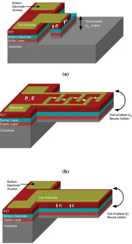
the longitudinal or the transverse piezoelectric response, respectively, is harnessed as explained in Figure 2.6. For thin film PZT, modest but potentially useful [88] surface displacements are generated in d33 mode, Figure 2.6(a). The d33 mode could also be
utilized in a flexural structure with interdigitated electrodes patterned on the PZT film, Figure 2.6(b). Applying an electric field between the electrodes, a modest in-plane strain can be induced in the plane of the film which leads to large out-of-plane displacements. Figure 2.6(c) shows the most commonly used d31 or e31 modes [2,6] to achieve large
28 (a)
(b)
(c)
Figure 2.6. Schematic of common sensing and actuation modes in piezoelectric MEMS. (a) Out-of-plane piston mode, (b) bending d33 mode, and (c) bending d31 or e31
29
In Figure 2.6(c), an electric field applied in the PZT thickness direction between the top and bottom electrodes induces strain in the thickness direction which, in turn, gives rise to in-plane strain. The unimorph structure then bends due to the mechanical asymmetry of the structure about the piezoelectric layer. Since the thickness of the PZT films used in this study was only 500 nm, the d31 mode was utilized.
In this dissertation research, cantilevers with d31 configuration were fabricated. As
described in Chapter 1, the piezoelectric coefficient d31,f depends on several factors, such
as chemical composition, nature and type of interfaces, grain orientation and texture, film thickness, and residual stresses. Although several attempts were made in the past to measure d31 of PZT thin films, by measuring the charge generated by a laterally deformed
PZT film on a Si wafer [29,90] or from the out-of-plane deflection of PZT cantilevers, universally accepted standard methods for the evaluation of the piezoelectric coefficient,
d31 have not been established yet. The following Section describes the experimental
methods used in this study to determine the ferroelectric and dielectric parameters of the PZT films at hand. Details about the fabrication of the PZT stacks and Pt films are provided in the respective Chapters in this dissertation.
2.3.1 Measurement of Ferroelectric and Dielectric Properties
Periodic oscillation of cantilever arrays fabricated from PZT stacks was induced by applying triangular wave voltage signals between the upper and bottom Pt electrodes in PZT stacks. Then, non-contact displacement measurements along the length of each cantilever were measured using a Polytec MSV-400 microscope scanning laser Doppler vibrometer (LDV) described in the schematic in Figure 2.7. The LDV was made available for this research by the US Army Research Laboratory (ARL) in Adelphi, MD. The out-of-plane displacement resolution of the LDV system was ~10 nm with a lateral resolution of ~2 µm using a 20× objective lens. An internal function generator created the triangular wave signals at 2 Hz, which is much lower than the mechanical resonant frequencies of the cantilevers, which are of the order of 100s of kHz. Voltage was applied to the top electrode while the bottom electrode was grounded. The out-of-plane
30
displacement and velocity were obtained using an interferometer that utilized a helium neon laser, which compared the reflected laser beam to a reference beam. The frequency and phase difference provided the instantaneous velocity and displacement, respectively. The displacement values along the length of the cantilevers were used to calculate the transverse piezoelectric properties of the textured freestanding PZT films. Additionally, polarization vs. electric field (P-E) hysteresis loops were measured at 100 Hz using a Radiant Technologies RT-66A measurement unit, and capacitance versus voltage (C-V) sweeps were performed using the Agilent Technologies B1500A device analyzer.
Figure 2.7. Displacement and velocity measurement principles using an LDV. Figure adapted from [91].
31
2.4 Summary
The experimental methods employed to achieve the objectives of this dissertation research, outlined in Chapter 1 were presented and discussed. A custom built modular tensile testing apparatus was employed to study the mechanical response of Pt films and PZT film stacks in the wide range of strain rates 10-6 – 101 s-1. Uniaxial tension experiments were performed under an optical microscope, and DIC was employed to compute local displacements with a resolution of ~25 nm. An LDV setup was used to measure out-of-plane deflections of microfabricated cantilevers which were then used to compute ferroelectric and linear piezoelectric coefficients of textured PZT.
32
CHAPTER 3
Mechanical Behavior of Epitaxially Grown {111}
Textured Pt Films
Pt thin films with thicknesses ranging between 50 nm and 8 µm [92] are frequently used as contact electrodes in piezoelectrically actuated MEMS. Most high conductivity metals, such as Al or Au, have a low melting point and hence low thermal stability and show creep deformation even at room temperatures [93,94]. High melting point materials, such as Ti and Ta, suffer from decreased chemical inertness and higher electrical resistivity. On the other hand, Pt is a relatively hard material with high melting point (Tm~1768°C), good conductivity and excellent chemical resistance. It is, therefore, utilized either as structural or contact material in MEMS devices with high resistance to plastic deformation at elevated temperatures while providing good electrical conductivity [95]. In connection with PZT materials, Pt films provide a sharp interface that suppresses diffusion of Pb and prevents the formation of lead silicate phases which would otherwise leach Pb from the ferroelectric and severely degrade its electrical properties [96]. It was recently shown that {001}-textured PZT with high transverse piezoelectric coefficient could be grown on a {111}-textured Pt layer [97]. Thus, piezoelectric properties which are strongly crystal structure dependent [30] may be tuned with appropriate choice of Pt film texture leading to an enhancement of PZT-based MEMS performance.Previous studies on the mechanical behavior of Pt thin films utilized various techniques including resonance [75], nanoindentation [68-72] and uniaxial tension [67,98]. Salvadori et al. [75] measured the resonance frequencies of atomic force microscope (AFM) cantilevers before and after coating them with Pt films with thicknesses between 18 and 73 nm; the authors used beam theory to determine the elastic
33
moduli of Pt as 139.7 ± 2.7 GPa. Mencik and Swain [68, 69], Lee et al. [70], Hyun et al. [71], and Romasco et al. [72] applied instrumented nanoindentation to quantify mechanical properties of Pt thin films with thicknesses in the range of 200 - 1500 nm and reported elastic moduli in the range 154 - 190 GPa. Jonnalagadda et al. [67] performed uniaxial tension tests at strain rates between 10-6 - 101 s-1 on 400 nm thick freestanding Pt films and reported an elastic modulus of 182 ± 8 GPa. They also showed that inelastic properties of nanocrystalline Pt films were rate-sensitive with tensile strength reaching almost 2 GPa at the fastest strain rate of 10 s-1 which is several times that of bulk, large grain Pt. Meirom et al. [98] also performed uniaxial tension tests on 460 nm thick freestanding Pt films and reported an elastic modulus of 158 ± 5 GPa with a yield strength of 1.5 ± 0.1 GPa and ultimate strength of 1.75 ± 0.05 GPa.
Most previous studies on Pt thin films were concentrated on a single film thickness or treated different thicknesses individually providing no correlation between film thickness, grain size, and mechanical response. Furthermore, the available literature on Pt thin films [68-70] has not always documented the details about film structure, i.e. film texture and grain size, which makes it difficult to establish the interplay between microstructural parameters in the mechanical response of Pt thin films.
Experiments with other face-centered cubic (FCC) Ag, Al, Au, Cu, Ni, Pb films with thicknesses of 50-2,000 μm have shown that the flow stress increases with decreasing film thickness [26-28,60,61,99-102]. In the case of metal films deposited on substrates, mechanistic models have been developed to explain this inverse film thickness dependence of flow stress. Based on the threading dislocation concept by Freund for a film bonded to a substrate with some mismatch strain [54], Nix [55] developed a quantitative model considering the film/oxide and film/substrate interfaces acting as impenetrable obstacles to dislocation motion, thus necessitating the deposition of misfit dislocations at interfaces. Later, Thompson [56] extended the Nix-Freund model to polycrystalline films with grain diameters that are at least twice as large as the film thickness by including grain boundaries (GBs) as additional obstacles to dislocation motion. The two models combined could qualitatively explain the inverse film thickness and grain size dependence of flow stress that was reported for Al films deposited on Si
34
substrates with an anodic oxide layer at the top surface [27]. Both the Nix-Freund and the Thompson models showed that the film texture influenced the yield stress.
The Nix-Freund model could quantitatively capture the flow stress of epitaxial metal films. Furthermore, epitaxial film-substrate interfaces acted as dislocation sources, and dislocation half-loops were emitted from the interfacial dislocation network. In contrast, no such phenomena were observed in polycrystalline films deposited on amorphous oxide or nitride layers on Si substrates. The amorphous underlayers did not promote the formation of stable interfacial dislocation networks because they permitted atomic rearrangements at the interface, thus allowing for dislocation segments arriving at the interface to escape [59]. Consequently, in the absence of interfacial dislocations, the Nix-Freund or the Thompson model underestimated the flow stress in polycrystalline films deposited on amorphous layers [60,61] where initiation of plastic deformation is delayed due to the scarcity of dislocation sources.
Von Blanckenhagen et al. [57] used the aforementioned idea to model the deformation response of polycrystalline metal films. They considered dislocation sources in polycrystalline metal films to be rare and, therefore, each Frank-Read source inside a grain had to operate several times to generate more dislocations and achieve the resulting plastic deformation. Their approach using discrete dislocation dynamics reproduced the experimentally measured flow stresses in polycrystalline Cu films deposited on amorphous and deformable polyimide layers. Thus, the underlying layer plays a major role in determining the plastic deformation of metal films: source controlled deformation models work well for polycrystalline films in the absence of interfacial dislocation networks, whereas epitaxially grown single crystal metal films are well described by the Nix-Freund model. However, there are hardly any studies on the deformation behavior of polycrystalline metal films grown epitaxially on polycrystalline layers. Although many metal films are deposited on amorphous diffusion barrier layers that are on top of single crystal silicon to prevent the formation of metal silicides [103,104], there are cases when polycrystalline metal films were grown epitaxially on polycrystalline layers in order to achieve specific textures [105]. The deformation behavior of such films is expected to be significantly different than of those films deposited on amorphous layers. Furthermore,
35
the Nix-Freund or the Thompson models which should be applicable to epitaxially grown metal films do not model the evolution of flow stress with plastic strain.
This dissertation investigated the inelastic response of highly {111}-textured epitaxial polycrystalline Pt films grown on 35-50 nm thick (100)-textured polycrystalline rutile TiO2 underlayers. Specifically, this research focused on relationships between the film thickness, grain size, strain rate and the plastic mechanical response of textured Pt films in the form of bilayers with an underlying TiO2 seeding layer and total thicknesses ranging between 50 nm and 1000 nm. The role of high aspect ratio columnar grain structure, which is not captured by previous models, was also addressed. To this goal, existing dislocation-based mechanistic models, modified to account for strain hardening, were applied to predict the evolution of flow stress with plastic strain and were compared with the experimental measurements obtained in this research.
3.1 Experimental Methods
3.1.1 Specimen Preparation and Materials Characterization
Micro and nanometer thick freestanding Pt film specimens were fabricated at the US Army Research Laboratory (ARL) in Adelphi, MD using a combination of DC magnetron sputtering and etching on Si (100) substrate. The fabrication process, described in detail in [106], began with the deposition of a base layer of Ti on a 500 ± 25 nm thermally grown SiO2 layer on a silicon wafer to serve as an adhesion layer using DC magnetron sputtering with a 99.99% pure Ti target at 40˚C. The Ti films had a strong {0001} texture with the basal plane of hexagonal close-packed (HCP) structure lying in the plane of the substrate. The Ti films were then converted to rutile through oxygen annealing for 30 minutes inside a tube furnace at 750˚C. The TiO2 films had measured thicknesses of 35 nm and 50 nm, and X-Ray diffraction studies showed (100) texture for TiO2. Next, sputter deposition of Pt was carried out for thicknesses of 1000, 500, 200, 100 and 50 nm onto the TiO2 with a 99.99% pure Pt target at a substrate temperature of 500°C as shown in step (A) in Figure 3.1(a). The resulting {111}Pt||(100)TiO2 grain-to-grain heteroepitaxy has been established before for 100 nm thick Pt films [105,106] with
![Figure 1.2 (a) Dielectric constant, dissipation factor, and piezoelectric strain coefficient as a function of residual stress: the piezoelectric and dielectric properties increase with decreasing residual stresses [36]](https://thumb-us.123doks.com/thumbv2/123dok_us/11108808.2998651/15.918.286.681.105.413/dielectric-dissipation-piezoelectric-coefficient-piezoelectric-dielectric-properties-decreasing.webp)

![Figure 1.5 Dislocation half-loops in single crystal epitaxial Cu films on Al 2 O 3 substrate, originating in the film/substrate interface and expanding during thermal cooling [26]](https://thumb-us.123doks.com/thumbv2/123dok_us/11108808.2998651/21.918.171.798.343.662/figure-dislocation-epitaxial-substrate-originating-substrate-interface-expanding.webp)


![Figure 2.7. Displacement and velocity measurement principles using an LDV. Figure adapted from [91]](https://thumb-us.123doks.com/thumbv2/123dok_us/11108808.2998651/37.918.199.750.434.786/figure-displacement-velocity-measurement-principles-using-figure-adapted.webp)


