Introduction
Two greatest research devices developed primarily for nuclear physics: nuclear reactors and charged particle accelerators are nowadays employed mostly outside of the field. Whereas nuclear reactors are used for electrical power generation, accelerators working in the energy range below 1 GeV are currently used in medicine as well as materials research and technology. In this review we will focus on the last issue.
Magnetic mass separators emerged as a by-product of American nuclear project during the World War II. Following the pioneer work of Chalk River Labor-atories in Canada and Harwell Nuclear Centre in UK at the beginning of 1960-ties they were further developed into the new class of accelerators: ion implanters [8]. Ion implanter is an electrostatic accelerator capable to produce intense ion beams at energies typically between 100 keV and 500 keV. Its ability to implant almost any kind of atom in the high purity vacuum environment was rapidly recognized by research and industry as an efficient tool for modification of solids. Semiconductor technologists and metallurgists were among the first users of this technique. Ion implantation is nowadays well established technological step of many modern industrial processes.
MeV accelerators remained the domain of nuclear physics till the mid-sixties of the last century. Depletion of research programmes in the nuclear basic research opened almost unlimited access to accelerators to the other users. Fortunately, in the same time silicon surface barrier detectors became available. Moreover,
Accelerators in materials research
Andrzej TurosA. Turos
Institute of Electronic Materials Technology, 133 Wólczyńska Str., 01-919 Warsaw, Poland and The Andrzej Sołtan Institute of Nuclear Studies, 05-400 Otwock-Świerk, Poland,
Tel.: +48-603-092223, Fax: +48 22-8645496, E-mail: [email protected] Received: 1 July 2005
Abstract Since at least forty years accelerators of charged particles no longer belong to nuclear physics exclusively. This is especially true for accelerators at energies below 1 GeV. The vast majority of accelerators in this energy range is used for materials research and medicine. In materials research the applications are principally twofold: modifications of solids and surface layer microanalysis.
Two most important challenges for materials research at the beginning of XXI century as determined by the Materials Research Society are: development of materials able to repair human body and development of materials for new electronic devices able to cope with the enormous amount of information to be stored and transmitted. The role of accelerators with regard to the challenges of modern technology will be discussed.
rapidly expanding semiconductor industry urgently demanded new methods of surface layers analysis. All these factors produced a strong driving force for merging the experimental skills of nuclear physicists with the solid state physics and technology. As a con-sequence, a powerful analytical technique of ion beam analysis was born [1, 17, 19, 20].
Ion beam modification of materials Ion implanters
Modification of surface regions of solids using ion beams can be divided into two groups. The first one is the classical ion implantation employing low energy ion implanters. These low energy accelerators are specially designed to produce high intensity ion beams that can be easily distributed over large area samples. They are usually equipped with different types of ion sources in order to be able to deliver a great variety of ion species. The typical acceleration voltage of an implanter ranges from 50 kV to 300 kV. The delivered beam power can be as high as 25 kW.
The other class of high current accelerators emerged in the second half of 1980-ties following the develop-ment of a new type of tandem accelerators. They are typically equipped with the sputter type ion sources that make it possible to produce virtually any kind of ions. With the terminal voltage up to 6 MV tandem acceler-ators are capable to deliver multiple charged heavy ions of energies well above 100 MeV. There are actually two companies that share the world market of such acceler-ators: High Voltage Engineering in the Netherlands and National Electrostatics Corp., USA. The principles of accelerator operation and other details can be found on their websites: www.highvolteng.com and www.pelletron.com, respectively.
Principal applications of ion implantation Doping of semiconductors
The introduction of dopants in a semiconductor is the most common application of ion implantation. In the case of silicon dopants are either group III atoms such as boron, phosphorus or group V atoms like arsenic. When implanted in a semiconductor, each dopant atom creates a charge carrier thus modifying the conductivity of the semiconductor to p-type or n-type.
Each incident ion collides with target atoms, resulting in a transfer of some amount of energy to the knocked-on atom such that it leaves its crystal site. This target atom then itself becomes a projectile in the solid, and can cause successive collision events. As a consequ-ence many point defects in the crystal such as vacancies and interstitials are produced. These point defects can migrate and cluster with each other, resulting in disloca-tion loops and other defects. Because ion implantadisloca-tion caused damage usually precludes electrical activity of implanted dopants subsequent thermal processing is necessary to achieve the damage recovery.
Silicon-on-insulator (SOI)
The Metal-Oxide-Field-Effect-Transistors (MOSFET) are widely used in large-scale digital integrated circuits (IC’s) where their high input impedance can result in very low power consumption per component [3]. Principle of the MOSFET is shown in Fig. 1a.
− Silicon-on-insulator (SOI) circuits consist of ICs which employ silicon-islands isolated from the substrate (and each other) by an underlying dielectric region. Each island contains a single transistor. Figure 1b is a schematic depiction of a MOSFET fabricated on an SOI wafer. Note that a buried-oxide exists beneath each device, providing vertical isolation. SOI is being intensely developed because it offers a number of significant advantages over bulk-CMOS technology, especially as devices scale below 100 nm. These are: lateral and vertical isolation of active devices from the substrate. This results in reduction of power-consumption and allows faster performance.
SOI wafers are produced by one of two main methods, both of which rely on ion implantation:
− SIMOX − Separation by IMplantation of OXygen: oxygen can be implanted at high energy into a silicon substrate, at a high enough dose that subsequent high temperature annealing forms an oxide layer underneath the surface layer of silicon. The oxide is an insulator, thus producing a silicon on insulator (SOI) structure.
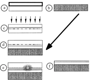
− Smartcut − this process is illustrated in Fig. 2. First, oxidized surfaces are grown on two wafers (Figs. 2a,b), and then in one of waters 1016/cm2 of Fig. 1. Schematic presentation of field effrect transistor (FET) structure: a − classical MOSFET, b − MOSFET on SOI.
a
hydrogen ions are implanted at energy 150−200 keV (Fig. 2c), subsequently wafers are bonded together as shown in Fig. 2d. Upon heating at 600°C most of the top wafer is cleaved away along a band of hydrogen bubbles which form from implanted ions (Fig. 2e). The thin layer of silicon that is left behind is isolated from the substrate by what were originally the surface oxide layers (Fig. 2e).
Steel tool toughening
To the date this is the most important application of ion beams to metals. Ion implantation of tools to improve their wear resistance is a very promising alternative to hard coatings. Mostly nitrogen ions are implanted into a steel tools especially those for cutting and forming like broaches, milling cutters, gear-shapers, drills, etc. The structural change caused by the implanta-tion produces a surface compression in the steel, which prevent crack propagation and thus makes the material more resistant to fracture. The chemical change can also make the tool more resistant to corrosion. Further advantage of this technique is the possibility to irradiate complicated, well developed surfaces.
Figure 3 shows an example of a cutting tool subjected to such a treatment. 80 keV N ions were implanted to the fluence of ranging from (1–5) × 1017 N/cm2 at RT [10]. An outstanding result of this treatment is shown in Fig. 4. The important increase of the total lifetime of tested tools is clearly visibly, however, there is an optimal implantation fluence of 3 × 10¹⁷ N/cm2. The overall increase of the lifetime of about 60% is an important factor for the industry. This beneficial effect has been attributed to the formation of the new phase of iron nitride namely ξ–Fe2N.
Modification of biomaterials
In the contemporary total joint arthroplasty, in which the total diseased joint has been replaced, metal-on-UHMWPE total joint replacement is an international standard [4]. Ultrahigh molecular weight polyethylene
(UHMWPE) is the material of choice for the load bearing surfaces of total joint implants. Selection of UHMWPE is due primarily to the combination of properties such as high abrasion resistance, high toughness, low coefficient of friction, good chemical resistance and relatively low cost. Unfortunately, failure is often observed caused by the UHMWPE fragility. Despite the recognized success a major obstacle limiting the lifetime of implants is osteolysis induced by wear debris produced in the form of microparticles from the surface of UHMWPE component. Microparticles are typically released from the microcracks generated by dynamical loads on the joint. Numerous efforts to solve the wear problem have revealed the necessity of UHMWPE modification, which is usually performed using different physical and chemical techniques leading to material crosslinking.
Fig. 2. Smartcut process.
a b
c
d
e f
Fig. 3. Special tool used in tests.
beam
Advantage of ion bombardment is the high stopping power of incident particles and limited, easily controlled range. Hence, by the judicious choice of implantation conditions the properties of near surface region up to several micrometers thickness can easily be tailored. Bombardment with light ions, like H or He, by pro-ducing primarily ionization and little displacements promotes crosslinking and are at best suitable for production of a hard layer [2, 18]. The increase of UHMWPE hardness due He-ion bombardment is shown in Fig. 5. The performed scratch tests clearly demonstrated that up to very high loads no cracks were formed. The reason most probably is the formation of a hard layer on the top of softer, unmodified material. Since the soft material can act as a shock absorber the response to dynamic load of such a structure can be significantly improved.
For more detailed description of various ion beam techniques applications the reader is referred to the Proceedings of the consequtive Conferences on Ion Beam Modification of Materials [11, 12].
High-energy accelerators
High-energy accelerators used in materials research are electrostatic accelerators of either single-end or tandem type. They can be typically applied for deep or ion beam analysis. Ion implantation at high energy is performed according to the rules presented earlier. The virtue of high energy is that it makes it possible to perform ion implantation to much greater depths. By employing multiple charged heavy ions energies over 100 MeV can be reached. At such energies LET of heavy ions attains extremely high values exceeding 10 keV/nm. As a consequence new physical effects like latent track formation take place. The most spectacular use of this effect is the production of nanopores and nanofilters that can be used for filtering of very small objects like bacteria, etc.
Ion beam analysis
Ion beam analysis (IBA), also called in its early days nuclear microanalysis, was born by the advent of semiconductor surface barrier detectors (www.ortec-online.com/detectors). They made measurement of energy spectra of charged particles and photons an easy and swift task.
This is based on the measurement of energy spectra produced by the interaction of incident beam (usually light ions like H or He) with analyzed sample [6, 16]. The interaction products are primarily charged par-ticles. The principal techniques are:
• RBS – Rutherford Backscattering Spectrometry is based on elastically scattered incident ions; this technique provides an easy way for detection and depth profiling of elements with atomic mass above 20. When combined with ion channeling can be used for single crystal analysis especially for defect depth distribution determination and impurity atoms lattice site location.
• NRA – Nuclear Reaction Analysis makes use of charged particles produced by nuclear reactions, mostly useful for detection and profiling of light elements. It makes also use of gamma rays emitted by nuclear nuclei produced by nuclear reactions. This branch is usually called PIGE – particle induced gamma-ray emission.
• ERDA – Elastic Recoil Detection Analysis here recoiled target atoms ejected from the sample by the impact of incident ions are detected; mostly used for depth profiling of light and medium atomic mass ions. Incident particle are usually high energy, i.e. above 30 MeV heavy ions.
• PIXE – Particle Induced X-ray Emission is based on detection of characteristic X-ray photons. In contrast to other technique, PIXE is not depth sensitive, its main virtue is very high sensitivity (detection limit can be as low as 10−8 g/g). PIXE can be applied for elements with atomic number Z >12. All these techniques are rather insensitive to atomic bonding, thus unable to provide chemical information. On the other hand, this is one of their biggest advantages because they are not affected by matrix effects and can provide results in absolute numbers. They are either internally calibrated, i.e. do not need an external ref-erence standard or can be calibrated by almost any suitable reference sample.
Because of the limited range of incident ions, which usually do not exceed a few µm IBA is the surface layers analysis technique. With respect to a vast majority of analyzed materials it is undestructive technique pre-dominantly applied for depth profiling of layered structures and atomic transport phenomena studies [9]. The main domain of IBA applications is modern high technology like micro- and optoelectronics, metallurgy, electrochemistry of solids, etc. Moreover, PIXE is frequently applied in environmental, biological and geological research. With the advent of nanotech-nology special IBA techniques were developed that make it possible to focus ion beams on the very small spots. It has been usually achieved by using special ion optics system allowing compressing ion beam down to
Fig. 5. Hardness improvement in low density polyethylene (LDPE) and ultrahigh density polyethylene (UHMWPE) upon 130 keV He-ion bombardment to different fluences.
250 nm diameter [7, 21, 22]. The other approach has been opened by development of nuclear emission spectro-scopies, which make it possible to visualize the impact points of single ions on the sample surface [5, 15].
The principal virtues of IBA can be summarized as follows:
− the analysis is quantitative, the measurement accuracy is better than a few per cent,
− depth resolution of 5 nm can be achieved,
− detection limits depend strongly on the sample composition but typically are of the order of 1015 at/cm2,
− lateral resolution, which is usually of the order of 1 mm can be scaled down to 250 nm using micro-beam systems.
The detailed description of all branches of IBA is beyond the scope of this review. Hence, only the most important issues has been presented. For more detailed description of various ion beam analysis techniques, the reader is referred to the Proceedings of the consequtive Conferences on Ion Beam Analysis [13, 14].
Conclusions
Rapid development of ion beam techniques for materials modification and analysis is one of the most spectacular examples of the strong feedback between industry and basic research. Strong driving force over last four decades has been hi-tech industry continuously demanding new dedicated techniques of higher and higher precision and sensitivity. Accelerator based technique were able to keep the pace. This was, however, only possible due to concentrated efforts of the basic research in the field of beam-solid interaction. The stagnated by end of the sixties last century the domain of atomic collisions in solids has got new inspirations and affluence of young talented researchers. The skilled technicians followed.
Nowadays ion beam techniques are indispensable steps in a variety of major technological processes. Although the complete technological processes cannot exclusively rely on these techniques their replacement would be expensive and ineffective.
Acknowledgment The author would like to express his gratitude to G. Gawlik and J. Jagielski (ITME), R. Ratajczak and A. Stonert (IPJ) for their support in preparing this review and J. Piekoszewski and Z. Werner (IPJ) for supplying the data on tool toughening.
References
1. Amsel G, Nadai J, d’Aretemare E, David D, Girard E, Moulin J (1971) Microanalysis by the direct observation of nuclear reactions using a 2 MeV Van de Graaf accelerator. Nucl Instrum Meth 92:481−485
2. Bieliński D, Lipiński P, Ślusarski L et al. (2004) Surface layer modification of ion bombarded HDPE. Appl Surf Sci 564:179−186
3. Colinge JP (2004) Silicon on insulator technology, 3rd ed. Kluwer Academic Publishing, Boston MA
4. Costa L, Luda MP, Trossarelli L et al. (1998) Oxidation in orthopaedic UHMWPE sterilized by gamma-radiation and ethylene oxide. Biomaterials 19:659−668
5. Doyle BL, Walsh DS, Renfrow SN, Vizkelethy G, Schenkel T, Hamza AV (2003) Nuclear emission spectro-scopies. Nucl Instrum Meth B 181:199−210
6. Feldman LC, Mayer JW (1986) Fundamentals of surface and thin film analysis. North-Holland, New York 7. Fischer BE, Heiss M, Cholewa M (2003) About the art
to shoot with single ions. Nucl Instrum Meth B 210:285−291
8. Mayer JW, Eriksson L, Davies JA (1970) Ion implanta-tion in semicondutors. Academic Press, New York 9. Mayer J, Turos A (1973) Comparison of surface layers
analysis techniques. Thin Solid Films 19:1−10
10. Narojczyk J, Werner Z, Piekoszewski J, Szymczyk W (2005) Effects of nitrogen implantation on lifetime of cutting tools made of SK5M tool steel. Vacuum 78:229−233
11. Proceedings of the XIIth Int Conf on Ion Beam Modification of Materials (2000) Nucl Instrum Meth B 161/163:1−1213
12. Proceedings of the XIIIth Int Conf on Ion Beam Modification of Materials (2003) Nucl Instrum Meth B 206:1−1143
13. Proceedings of the XVth Int Conf on Ion Beam Analysis (2002) Nucl Instrum Meth B 190:1−906
14. Proceedings of the XVIth Int Conf on Ion Beam Analysis (2004) Nucl Instrum Meth B 219/220:1−1084
15. Rossi P, Doyle BL, Banks JC et al. (2003) Ion photon emission spectroscopy. Nucl Instrum Meth B 210:123−128
16. Tesmer J, Nastasi M (eds) (1995) Ion beam analysis handbook. MRS, Pittsburg
17. Turos A (1978) Near surface analysis of solids using ion beam techniques. Nukleonika 23:183−207
18. Turos A, Jagielski J, Piątkowska A, Bieliński D, Ślusarski L, Madi NK (2002) Ion beam modification of surface properties of polymers. Vacuum 70:201−205
19. Turos A, Wilhelmi Z (1968) Applications of the Coulomb backscattering of heavy charged particles. I − Thickness measurements of thin foils and surface layers. Nukleonika 13:991−997
20. Turos A, Wilhelmi Z (1969) Applications of the Coulomb backscattering of heavy charged particles. II − Chemical analysis of surface layers. Nukleonika 14:319−335 21. Watt F (1997) The nuclear microprobe: a unique
instru-ment. Nucl Instrum Meth B 130:1−8
22. Watt F, van Kan JA, Rajta I et al. (2003) The National University of Singapore high energy ion nano-probe facility: performance tests. Nucl Instrum Meth B 210:12−20