VL·7709a
VL·7709b
VL·77CT09a
VL·77CT09b
64/256K
Memory Card
NOTICE:
Model VL-7709
64/256K
Memory Card for the
sro
Bus
REFERENCE MANUAL
VL-7709a VL-7709b VL-77CT09a VL-77CT09b Doc. Rev.
Rev. 1.00 Rev. 1.01 Rev. 1.00 Rev. 1.01 9/10/93
VersaLogic Corporation
3888 Stewart Rd. • Eugene, OR 97402 (503) 485-8575
Fax (503) 485-5712 Contents Copyright 1993
All Rights Reserved
Although every effort has been made to ensure this documentation is error-free, VersaLogic makes no representations or warranties with respect to this product and specifically disclaims any implied warranties of merchantability or fitness for any particular purpose.
Model VL-7709 64/256K Memory card
REFERENCE MANUAL
1. Overview Introduction OVerview Features Description • Specifications
2. Operation
CONTENTS
Introduction . . . . Selecting an Address Mode
Address Bus
Memory Chip Selection Bank Selection
Using MEMEX
Battery Backup
Write Protection Switches
3. Installation
Handling
Installation • . . . External Connections
4. Configuration
Jumper Summary
Memory Configuration
16-Bit Address • . . • • • • • •
16-Bit Address With 8K Chips 64K Bank
32K Banks
16-Bit Address With 32K Chips 64K Banks
32K Banks
1-1 • 1-1
1-2 1-2 1-4
2-1 2-1
2-4 2-6
3-1 3-1 3-2
• 4-1 • 4-4 • 4-5
4-12 20-Bit Address . . . .
20-Bit Address With 8K Chips 20-Bit Address With 32K Chips
Memory Socket Configuration • Disabling Unused Sockets Chip Power Selection Bank Control Port Address Battery Backup Source • . • •
5. Reference
VL-7709 Parts Placement Diagram VL-7709 Schematic
VL-7709 Parts List VL-7709B Parts List VL-77CT09 Parts List VL-77CT09B Parts List
STD Bus Pinout ASCII Table
Contents Copyright 1991 All Rights Reserved
VersaLogic Corporation 3888 Stewart Rd. Eugene, OR 97402
(503) 485-8575
4-17
Section 1
Section 1 OVERVIEW
INTRODUCTION
Overview
This manual details the installation and operation of VersaLogic's
VL-7709 memory card. The VL-7709 card accepts 8K or 32K RAM and ROM
devices, and is available with battery backup option for totally non-volatile operation. It features 16 and 20 bit addressing, and is compa-tible with all common STD Bus processor types. It is fully compatible with the Pro-Log 7709 memory board.
The "B" versions of the board (VL-7709B, VL-77CT09B) include an on-board backup battery and related support circuitry.
Throughout this manual "VL-7709" will be used to refer to all versions of the board, unless specifically noted otherwise.
OVERVIEW
The VL-7709 memory card includes eight 28-pin JEDEC sockets which can be jumpered to accept 8K or 32K memory chips. This provides a capacity of 64K (with 8K chips) or 256K (with 32K chips) of memory. RAM and ROM chips (of a similar size) can be mixed on the same board.
The board provides both 16-bit addressing (for Z80, 8085, etc.) and extended 20-bit addressing for use with STD 8088 systems. In addition, a programmable bank select port allows selection of multiple memory boards in 16-bit systems (in either 32K or 64K blocks). Multiple
VL-7709 boards (up to 1M byte) can be directly addressed in 20-bit systems.
The MEMEX signal is decoded for use with bootstrap applications, or for further extending the number of boards that can be addressed.
The battery backup option provides a completely self-contained data retention system for use in nonvolatile memory applications. The long life lithium battery, and complete power monitoring circuitry allow the on-board data to be retained for 5-10 years (depending on the chips used) with or without the presence of system power.
Write inhibit switches allow on-board RAM to be protected (to act as ROM) to simplify testing during software development.
Section 1 OVerview
FEATURES
- 64K to 256K byte capacity.
- Eight 28-pin JEOEC memory sockets. - Accepts 8K and 32K byte RAMs and ROMs. - 16-bit and 20-bit address decoding. - Bank select and MEMEX decoding. - Optional lithium battery backup. - Write inhibit switches.
- Extended temperature version available. - Universal STO Bus processor compatible. - Three year warranty.
DESCRIPTION
Addressing
Both 16 and 20-bit addressing are supported. The 20-bit mode is STO
8088 Bus compatible. It extends the system addressing capability by
strobing and latching A16-A19 from the 00-03 bus lines when operation with an 8088 CPU card. The 20-bit addressing mode allows large amounts of memory (1M bytes) to be directly addressed by the CPU.
The 16-bit addressing mode is compatible with most 8 bit CPUs (Z80, 8085, 6809, etc.). It includes a programmable memory bank control that allows these systems to address more than 64K of memory. 64 banks of 32K or 64K bytes of memory can be selected by the processor for up to 4M bytes of system memory. The Bank Control port can be addressed at any I/O location (OO-FF).
Both 16 and 20-bit addressing can be extended (capacity doubled) using the MEMEX signal which is also decoded by the VL-7709.
Memory Sockets
Eight 28-pin JEOEC compatible memory sockets accept either 8K or 32K byte RAM and ROMs. Each pair of sockets can be jumper configured for RAM/ZRAM/EEROM or ROM/PROM use, and whether or not they will be powered by the on-board battery (optional) when system power is not available. Each socket can be individually disabled to remove it from the memory map. The VL-7709 board has a capacity of 64K (8K chips) or 256K bytes
Section 1 Overview
Memory Chips
Memory chips used wLth the VL-7709 should be selected according to the capaci ty required (8K or 32K per socket), speed of the system CPU, and power required in standby mode (if the chip will be battery backed-up). The tables below detail these parameters.
Access Time (min.)
8085
6.25
MHz
415
zoo
4 MHz
200
ZOO
6 MHz
110
8088 8088
5 MHz 8 MHz
325 180 ns
Minimum RAM/ROM Access Times
8K RAM
Hitachi HM6264LP* (2uA)# Toshiba TC5564PL* (.01uA)#
8K PROM
Intel 2764A Intel 27C64-* Hitachi HN482764 Hitachi HN27C64* AMD AM2764A TI TMS2764
32K RAM
Hitachi HM62256LP* (2uA)# Toshiba TC55257PL* (2uA)#
32K PROM Intel 27256 Intel 27C256* Hitachi HN27256 Hitachi HN27C6256* AMD AM27256
* CMOS part.
#
Standby current rating.Typical Memory Devices
Memory Mapping
With 20-bit addressing the board can be located at any 64K (with 8K chips) or 256K (with 32K chips) boundary. With 16-bi t addressing the board can be configured as 64K of memory, 64K of bank selectable memory, or two overlapping 32K blocks of bank selectable memory.
Battery Backup
The battery backup option provides automatic backup power for on-board
RAMs. The high capacity lithium battery assures data retention for
short or long term outages (5-10 years). The backup circuitry also
monitors the system power level and protects on-board RAM from spurious writes during power up and power down. A board-edge LED indicator, and Battery Low output signal allow the condition of the battery to be
monitored if desired.
Section 1 Overview
SPECIFICATIONS
Size: Meets all STD Bus mechanical specifications.
Storage Temperature:
- VL-7709: -40· to +7S· C. - VL-77CT09: -40· to +8S· C.
Free Air Operating Temperature: - VL-7709: O· to +6S· C.
- VL-77CT09: -40· to +8S· C.
Memory Sockets: Eight 28 pin JEDEC compatible.
Power Requirements:
- VL-7709:
sv
±S% at lS0 rna typo (without on-board memory). SV ±S% at 17S rna typo (with 8 low power RAMs).- VL-77CT09: SV ±10% at 2S rna typo (without on-board memory). SV ±10% at 70 rna typo (with 8 low power RAMs).
Battery Type: Lithium.
Battery Voltage: 3.SV nominal (2.SV min.)
Battery Capacity: 7S0 mAR
Data Retention Time/ Battery Life (at 2S·C) :
- 64K bytes (8x8K chips) @ 2uA/chip: 4 years.
Section 2
Section 2
OPERATION
INTRODUCTION
Operation
Since the function of the VL-7709 board is simply to hold RAM or ROM for use by the system CPU, there is very little attention needed to the board once it is installed. However, since there are several ways that the board can be configured, careful thought should be given to the board's operation before it is installed in the system.
This section briefly discusses the various options that are available with this board including 16 and 20-bit addressing, bank selection, battery backup, and the write protection switches.
Details of configuring the board for these options can be found in Section 4 of this manual.
SELECTING AN ADDRESS MODE
Address Bus
The VL-7709 operates in two address modes, 16-bit (for Z80, 8085, 6800, 6500, etc. systems) and 20-bit (for STD 808S systems).
Most non-80S8 users will select the 16-bit bit addressing mode. In this mode up to 64K bytes of memory can be directly addressed. The bank selection feature can be used to allow so-ftware selection of additional 32K or 64K blocks of memory.
In the 20-bit mode, data lines DO-D3 act as address lines A16-A19 during part of the read/wri te cycle and are automatically latched by the VL-7709 board. Up to 1 M byte of memory can be directly addressed in this mode. Bank selection is not available.
Both addressing modes support the MEMEX control. This signal, which is usually controlled by the system CPU, allows a "main" and "secondary" memory area to be selected. It can be used for startup/bootstrap opera-tion, or to double the amount of accessible memory in a system. See Using MEMEX in this section for further information.
Memory Chip Selection
Before the board can be configured for the desired addressing and map-ping options, the type of memory chips to be used must be known. The VL-7709 supports both 8K and 32K byte types.
Only one size can be used on the board. 8K and 32K chips can not be mixed.
Section 2 Operation
The selection of memory chips will normally be based on current chip
pricing. An exception to this is in systems that will use larger
amounts of memory. 32K chips will usually be appropriate in these cases since 256K of memory can reside on a single board, versus only 64K bytes per board using 8K chips. The extra expense of 32K chips (if any) is usually outweighed by the expense of additional memory boards, bus slots, etc.
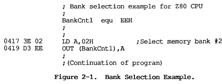
Bank Selection
In the 16-bit addressing mode the VL-7709 supports bank selection. This method of memory expansion allows the processor to switch a number of blocks (banks) of memory in and out of its basic 64K addressing space. When a bank is selected it takes its place in the addressing space and may be read and written in normal fashion. When a different bank is selected the memory on the old bank is no longer accessible by the CPU. The data is simply retained in the bank until it is once again selected by the CPU.
The VL-7709 allows a bank size of either 32K or 64K bytes. Depending on the bank size, and the type of chips used, each bank may be physically located on the same or different VL-7709 boards.
The process of selecting a bank involves simply writing a bank number to the Bank Control port (see example below). The desired bank is immedi-ately selected and the previously selected bank is de-selected. The VL-7709 board always selects bank 00 at power-up, or whenever the system is reset.
Note that for proper bank select operation the Bank Control port address (normally EE) must be the same on all memory cards in the system.
0417 3E 02 0419 D3 EE
; Bank selection example for Z80 CPU ;
BankCntl equ EEH
.
,
;LD A,02H
OUT (BankCntl),A
,
;Select memory bank #2
; (Continuation of program)
Figure 2-1. Bank Selection Example.
When using bank switching there are several special programming
consid-erations. Most important is maintaining software continuity when
switching banks. If the currently executing program is located in a
[image:10.597.81.458.476.619.2]Section 2 Operation
program counter and expects to read the next program instruction.
This software problem can be dealt with in several ways. First, by selecting a 32K bank size, only half of the memory map is switched in/out at a time. This allows the routine that does the bank switching to be located in a portion of the address space that is not being switched. A typical example is shown in Figure 2-2.
In this example the lower 32K of memory is fixed (not bank selectable). It holds the program code for bank swi tching so that the upper half of the map can be swi tched wi thout concern for program continui ty. Note that the lower 32K block must be configured for no bank selection so that it will not be switched out when the upper 32K~anks are selected.
F F F F 8
BANK
00
8000
7 F F F 6 SEE NOTE
1
0000
r::Jr::J
LJLJ
(1) Primary RAM or ROM. Contains bank switching routine.
Figure 2-2. Typical 32K Bank Switching.
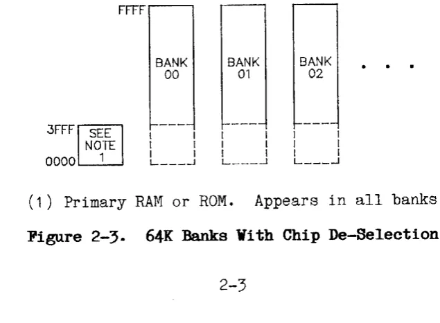
When 8K chips are used, a similar scheme can be employed by using 64K banks and de-selecting one or more chips at the bottom of each bank. This empty space in each bank can then be used for some non-bank selected memory (on a
VL-7709
or the system CPU board) that can reside at the bottom of the map. The figure below illustrates this approach.FFFF'----'
3FFF~EE
NOTE
0000 1
BANK
00
I I I I L ___ -l
BANK 01
I I
BANK
02
I I L ___ -l
(1) Primary RAM or ROM. Appears in all banks.
Figure 2-3. 64K Banks With Chip De-Selection.
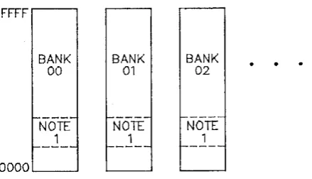
[image:11.595.93.478.260.453.2] [image:11.595.127.445.554.787.2]Section 2 Operation
Finally, full 64K banks can be used by placing a small section of identical code (the bank switching routine) in each bank. Figure 2-4 illustrates this scheme.
FFFF
BANK
00
-NorY
__ L_
OOOOL-_-l
BANK
01
BANK
02
(1) Bank switching routine (a copy in each bank).
Figure 2-4. 64K Bank Switching
Using MEMEX
The MEMEX (memory expansion) signal on the STD Bus can be used to select between two different memory banks or maps. It is simply another way to enable/disable certain memory board(s) in the system. It can be used to double the available memory (similar to selecting between two banks), or to control a bootstrap PROM (that disappears from the map after power-up). The MEMEX signal is usually controlled by (or jumpered to ground on) the system CPU card.
The VL-7709 decodes MEMEX in both the 16 and 20-bi t addressing modes. MEMEX is usually low (default) to select the standard or normal memory map. MEMEX high typically selects a secondary or alternate memory map. Boards that ignore the state of MEMBX will appear in both memory maps.
As shipped the MEMEX jumper (V2h) is set to ignore the MEMEX signal. The VL-7709 board will be addressed whether MEMEX is high or low. Refer to MEMEX Options in the Configuration section for further information.
Since the MEMEX signal causes program memory to be switched in and out of the CPU's address space, the same software cautions apply to using MEMEX as to bank switching in general (see Bank Selection above).
BATTERY BACKUP
[image:12.595.181.401.149.275.2]Section 2 Operation
The backup battery used on the VL-7709 is a long life lithium type. I t
does not require charging or setup prior to being placed in service.
The data retention (battery life) time for the battery depends primarily on the type of RAM chip used. Typical unpowered backup time is 4-10
years. Some examples are listed in Specifications in the Overview
section. Note that wi th extremely low power RAMs, the data retention calculation must be artificially limited since the shelf life of the battery is not guaranteed past 10 years.
The power backup of on-board chips is jumper selectable for each socket pair. Each chip pair may use standard (non-backed-up) system power, or automatically backed-up power. Be certain that only sockets using RAM chips are jumpered for backup power. Jumpering PROM chips for backup power will result in unnecessary battery drain and shortened battery life.
A low battery signal and on-board LED indi.cator are available to
indi-cate that the on-board battery is getting weak. The LED indicator,
which is located at the edge of the board, will light whenever the battery is low and the system power is on (the LED is powered by the system, not by the battery).
The low battery signal is available at connector J1 (see Figure 3-2). It is normally used for connection to an I/O card in the system for automatic monitoring of the battery condi tion. This signal goes low when the battery is getting weak. The low battery signal is valid only when the system power is on.
The low battery signal occurs when the battery output falls below 2.5 volts.
For special applications the power backup circuit may be connected to an external backup battery (instead of the on-board lithium cell). The external battery must be between
3.3
and4.5
volts. If required the VL-7709 can supply a charging current for this battery by installing the R-aPT resistor on the board.Section 2 Operation
WRITE PROTECTION SWITCHES
The VL-7709 provides four board switches that can write protect on-board RAM chips. The switches located at the board edge are accessible while the board is inserted in a card cage.
When the swi tch is up (off, open) the current contents of associated RAM chips can not be altered (written to) by the system CPU. This is useful during software development for simulating ROM based software, or for debugging software that overwrites itself in error. The switch can be set to the down (on) position at any time to allow writing to RAM.
Each write protect switch is associated with a pair of memory sockets. As shown below these pairs are identical to those controlled by the configuration jumpers (A-D).
Write Switch
A B C D
Controlled Sockets
MO, M1
M2, M3
M4, M5
M6, [VI7Section 3
Section 3
INSTALIATION
HANDLING
Installation
** CAUTION ** The VL-7709 card uses chips which are sensitive to static
electricity discharges. Normal precautions, such as discharging
your-self, work stations, and tools to ground before touching the board should be taken whenever the board is handled.
The board should also be protected during shipment or storage by placing it in a conductive bag (such as the one it was received in) or by wrapping it in metal foil.
INSTALIATION
The VL-7709 card can be installed in any slot of an STD Bus card cage.
The VL-7709 does not use the STD Bus priority interrupt chain. However, the priority IN and OUT pins on this board are connected together so that the priority chain will not be broken. This board may be inserted between other boards that are using the priority chain.
** CAUTION ** When cards are installed in an STD Bus card cage they must be oriented correctly (usually with the card ejector toward the top of the cage). Refer to the card cage documentation for the correct way to insert the STD Bus cards.
** CAUTION ** Cards should be inserted or removed from the STD Bus card cage only when the system power is off.
Note: VL-7709B versions (with battery backup) utilize a long life
lithium battery for the backup power source. This battery does not
require charging or other maintenance during installation.
Section 3 Installation
EXTERNAL CONNECTIONS
Connection to the low battery indicator signal (Jl) on the VL-7709B board can be made with the mating connector listed below. Connector Jl is a two-pin right angle header which is accessible at the outside edge of the board. Pin one, marked with a dot, is oriented nearest to the card ejector.
VL-7709B
Connector Mating Connector
Jl AMP #530554-1 + (2) #530553-5 or equiv. two-pin connector.
Jl
Pin
1
2
Figure 3-1. VL-7709B I/O Connector.
Signal
Name
GND
LOW BATTERY*
Output Drive (Sink rna)
5 rna
Section
4
Section 4
CONFIGURATION
JUMPER SUMMARY
Configuration
Various options available on the VL-7709 card are selected using re-movable jumper plugs (shorting plugs). Features are selected or de-selected by installing or removing the jumper plugs as noted. The terms "IN" or "JUMPED" are used to indicate an installed plug. "OUT" or "OPEN" indicates the absence of a jumper plug.
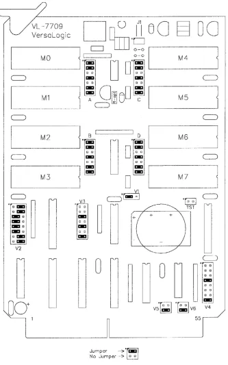
Figure 4-1 shows the jumper block locations on the VL-7709 board. It indicates the position of the jumper plugs as shipped from the factory. The function of each jumper block is detailed in Figure 4-2.
Section 4
VersaLogic
MO
M2
M3
c:=;J
"0-
o I:KI~
I:KI 0I:KI 0
I:KI 0
I:KI 0
" I:KI D I:KI V2
U
00+
0
Jumper ,-~
TEmI
No Jumper ""-~ D DM6
M7
Figure 4-1. Jumper Block Locations
Configuration
c:=;J
1 c:=;J
...
~
[image:18.595.129.463.131.665.2]Section 4
Jumper Description
Block
A-D Memory socket options. See Memory
Socket Configuration section.
Configuration
As
Shipped
All 8K RAMs
VI Battery backup source. (VL-7709B version)
a - Off-board (STD pin 5) . a - IN
b - On-board battery b - out
V2 Board Address. See addressing sections.
V3
V4
V5
V6
Memory map selection.
a, d, f - 32K parts in a 256K block.
b, e, g - 8K parts, 32K blocks, bank sel. c, e, g - 8K parts in a 64K block.
Bank Control port I/O address. See Bank Control Port Address section.
IOEXP select (for Bank Control port) . a - Active high.
b - Active low.
Don't care (both jumpers out) •
out out IN
Hex EE
a - out
b - IN
Addressing mode. a - 20-bit (8088)
b - 16-bit with bank select. - - 16-bit without bank select
a - out b - IN (no jumpers).
Figure 4-2. Jumper Functions
[image:19.595.90.506.58.440.2]Section
4
ConfigurationMEMORY CONFIGURATION
The V1-7709 has eight on-board memory sockets which can accommodate 8K or 32K byte RAM and ROM devices. RAMs and ROMs of the same size can be mixed on the board. Individual memory sockets can be disabled to remove them from the memory map.
The board can be addressed with 16 or 20-bit addressing with bank selec-tion available in the 16-bi t mode.
The jumpers needed to make these selections are detailed below. See the Operation section for more information on selecting and using these address modes.
Section 4 Configuration
16-BIT ADDRESS
The 16-bit addressing mode is available for use with most STD Bus sys-tems with 8-bit CPU cards including Z80, 8085, 6800, and 6500 types. In this mode up to 64K of memory can be directly addressed by the proces-sor. Bank selection, provided by the VL-7709 card, allows multiple banks of memory to be switched in and out of the CPU's address space. A new memory bank is enabled by wri ting to the Bank Control port. Up to 4M bytes of memory can be accessed by the CPU using this method.
To jumper the board for the 16-bit addressing mode set jumpers V4-V6 as shown below.
.-~
o 0
o 0 o 0
V4~
o 0 o 0Jumper Description
Block
V51~J
V2 Board Address and MEMEX.
Setting
Refer To Text
V3 Memory map selection. Refer To Text a, d, f - 32K parts, 256K block
V4
V5
V6
b, e, g - 8K parts, 32K blocks, bank sel. c, e, g - 8K parts, 64K block.
Bank Control port I/O address. See Bank Control Port Address for special configurations.
IOEXP select (for Bank Control port). a - Active high.
b - Active low.
- - Either (both jumpers out).
(Port EE) a-c - out
d - IN
e-g - out h -
IN
a - out b - IN
Addressing mode. a - 20-bit (8088)
b - 16-bit with bank select.
- - 16-bit without bank select (no
a - out
b -
IN
jumpers) •
Figure 4-3. 16-bit Address Mode Selection
[image:21.595.85.515.211.757.2]Section 4 Configuration
16-bit Address With 8K Chips
When 16-bi t addressing and 8K chips are used the board can hold up to 64K bytes of memory. This can be arranged as one 64K block (with or without bank selection), or two 32K blocks (at the same address) with bank selection. These options are discussed separately below.
64K Bank
When 16-bit addressing with 8K chips will be used in a single 64K block (the most standard configuration) set jumper blocks V2 and V3 as shown below.
If bank swi tching is not needed jumpers V2a-f should all be installed (bank zero). Otherwise jumpers V2a-f should be set to select the board for the desired bank number as shown in Figure 4-5. Figure 4-4 details the address of each memory socket on the board.
The Bank Control port is initialized to bank zero when power is appli.ed to the system. This will change only if data is written to the Bank Control port (I/O port EE as shipped). I f desired the Bank Control port can be disabled completely. Refer to the Bank Control Port Address
section for further details.
-This jumper configuration ignores the state of the MEMEX signal in
addressing the board. For systems that will use MEMEX, refer to the MEMEX Opti~ section.
Memory Socket
-0 1 2 3 4 5 6 7
0000- 2000- 4000- 6000- 8000- AOOO- COOO-
EOOO-1FFF 3FFF 5FFF 7FFF 9]<'PJ:<' B1<'FF DFFF FFFF
[image:22.595.100.507.434.516.2]Section 4 Configuration
• [Q..:9J 0 ~a
•
0 0[~=1JJ 0 ~b 0 0
rq:=:9J 0 ~c E:.:I
V2
[tf:1lJ [:I ~dV3
0 0[~=jJJ 0 ~e E:.:I
n~::=9J 0 ~f 0 0
o E:.:I E:.:I
o E:.:I
V2 Memory V2 Memory
a b c d e f Bank a b c d e f Bank
X X X X X X 00* X X X X X 20
X X X X X 01 X X X X 21
X X X X X 02 X X X X 22
X X X X 03 X X X 23
X X X X X 04 X X X X 24
X X X X 05 X X X 25
X X X X 06 X X X 26
X X X 07 X X 27
X X X X X 08 X X X X 28
X X X X 09 X X X 29
X X X X OA X X X 2A
X X X OB X X 2B
X X X X OC X X X 2C
X X X OD X X 2D
X X X OE X X 2E
X X OF X 2F
X X X X X 10 X X X X 30
X X X X 1 1 X X X 31
X X X X 12 X X X 32
X X X 13 X X 33
X X X X 14 X X X 34
X X X 15 X X 35
X X X 16 X X 36
X X 17 X 37
X X X X 18 X X X 38
X X X 19 X X 39
X X X 1A X X 3A
X X 1B X 3B
X X X 1C X X 3C
X X 1D X 3D
X X 1E X 3E
X 1F 3F
* Use bank 00 if bank switching will not be used. X
=
Install jumper in location shown- =
Remove jumperFigure 4-5. 8K Chip / 64K Bank Addressing
[image:23.595.62.512.75.678.2]Section 4 Configuration
32K Banks
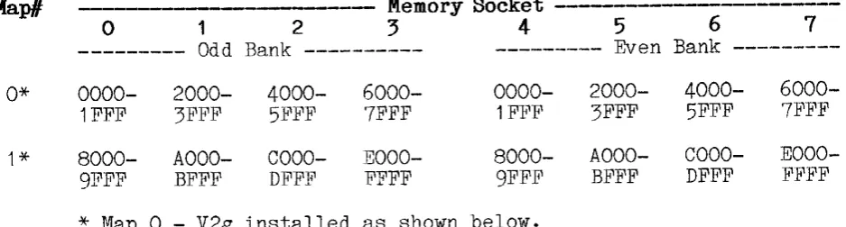
16-bi t addressing wi.th 8K chips can also be configured as two 32K memory banks. In this mode both 32K blocks occupy the same memory space, and switching between them is accomplished with the Bank Control port. To select this mode set jumper blocks V2 and V3 as shown below.
Jumpers V2a-e are used to select the board for the desired banks as shown in Figure 4-6. Jumper V2g is used to select one of the two memory maps detailed in Figure 4-6.
This jumper configuration ignores the state of the MEMEX signal in addressing the board. For systems that will use MEMEX, refer to the MEMEX Options section.
Map/l - - - - - - - Memory Socket
-o
1 2 3 4 5 6 7--- Odd Bank --- Even Bank
---0* 0000- 2000- 4000- 6000- 0000- 2000- 4000-
6000-1FFF 3FFF 5:B'FF 7FFF 1 FI<'F 3FFF 5FFF 7FFF
1* 8000- AOOO- COOO- EOOO- 8000- AOOO- COOO-
EOOO-91~FF BFFF DFF1~ FFFF 9FFF BFFF DFFF :B'FFF
* Map
o -
V2g installed as shown below. Map 1 - V2g removed. [image:24.595.65.534.276.402.2]Section 4 Configuration
• Lt!::9J [] -ra
•
[] [][tf::::p] [] -rb .-::I
Lif::::1JJ [] -rc [] 0
V2
[tI:::::9J [] -rdV3
0 0[tI::::1J] [] -re .-::I
[] .-::I 0 0
L~=:PJ [] -rg .-::I [] .-::I
32K BANK
V2 Memory Socket
a b c d e 0-3
4-7
X X X X X 01 00
X X X X 03 02
X X X X 05 04
X X X 07 06
X X X X 09 08
X X X OB OA
X X X OD OC
X X OF OE
X X X X 11 10
X X X 13 12
X X X 15 14
X X 17 16
X X X 19 18
X X 1B 1A
X X 1D 1 C
X 1F 1E
X X X X 21 20
X X X 23 22
X X X 25 24
X X 27 26
X X X 29 28
X X 2B 2A
X X 2D 2C
X ?1i1 ~~ 2E
X X X 31 30
X X 33 32
X X 35 34
X 37 36
X X 39 38
X 3B 3A
X 3D 3C
3F 3E
X = Install jU;'llper in location shown - = Remove jumper
:Figure
4-7.
8K Chip / 32K Bank AddressingSection 4 Configuration
16-Bit Address With 32K Chips
When 16-bi t addressing and 32K chips are used, up to four 64K banks of memory can be addressed on the board. Each pair of sockets is addressed as a different memory bank. Multiple boards can be used to address additional 64K banks of memory. By disabling every other socket, this same mode can be used to address 32K banks of memory (four per board).
64K Banks
To use 16-bi t addressing with 32K chips set jumper blocks V2 and V3 as shown below.
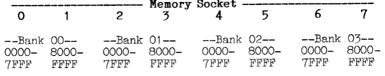
If bank swi tching is not needed jumpers V2a-d should all be installed (map 0) and only sockets 0 and 1 should be used. Otherwise jumpers V2a-d shoulV2a-d be set to select the boarV2a-d for the V2a-desireV2a-d bank number as shown in Figure 4-9. Figure 4-8 details the address and bank of each memory socket (example shown is for Map 0).
The Bank Control port is initialized to bank zero when power is applied to the system. This will change only if data is written to the Bank Control port (I/O port EE as shipped). If desired the Bank Control port
can be disabled completely. Refer to the Bank Control Port Address
secti on for further detai.ls.
This jumper configuration ignores the state of the MEMEX signal in addressing the board. For systems that will use MEMEX, refer to the MEMEX Options section.
o
1--Bank
00--0000-
8000-7FFF FFFF
2
Memory Socket
---3 4 5 6 7
--Bank
01--0000-
8000-7FFF FFFF
--Bank
02--0000-
8000-71"FF FF.FF
--Bank
03--0000-
8000-7FFF FFFF
[image:26.595.96.481.450.526.2]Section 4 Configuration
• [~_.9J 0 - 0 • r.::I
Li~L=~~U 0 <C--b 0 0
lfI:::::Ql 0 <C--C 0 0
V2
Lii~~J:!: 0 <c-dV3
r.::Io Ja::I 0 [1
[1 r.::I ~
[1 IBIl 0 D
D r.::I
MEMORY BANKS
---- V2 - - - Map# --Memory
Sockets--a b c d 0-1 2-3 4-5 6-7
X X X X 0* 00 01 02 03
X X X 1 04 05 06 07
X X X 2 08 09 OA OB
X X 3 OC OD OE OF
X X X 4 10 11 12 13
X X 5 14 15 16 17
X X 6 18 19 1A 1B
X 7 1 C 1D 1E iF
X X X 8 20 21 22 23
X X 9 24 25 26 27
X X A 28 29 2A 2B
X B 2C 2D 2E 2F
X X C 30 31 32 33
X D 34 35 36 37
X E 38 39 3A 3B
F 3C 3D 3E 3F
*
Use Map 0 if bank switching will not be used.X
=
Install jumper in location shown- =
Remove jumperFigure 4-9. 32K Chip / 64K Bank Addressing
32K Banks
The use of 32K chips in 32K banks is not specifically supported by the VL-7709. However, it can be easily accomplished by jumpering the board for 64K banks (see section above) and disabling every other socket (see Disabling Unused Sockets).
See the Operation section for general information on using bank selec-tion.
[image:27.595.156.430.40.461.2]Section 4 Configuration
20-BIT ADDRESS
The 20-bit addressing mode is available for systems using STD BOBB type processor boards. In this mode either 8K or 32K byte chips can be used
on board for a maximum capacity of 64K or 256K respectively.
20-bit addressing allows multiple VL-7709 boards to be used in a system, with the CPU directly addressing of up to 1M bytes of memory.
To jumper the board for the 20-bit addressing mode set jumpers V6 as shown be low.
Jumper Block
V2
V3
V4
V5
V6
Description
Board Address and MEMEX. Memory map selection.
a, d, f - 32K parts, 256K block b, e, g - 8K parts, 32K blocks, c, e, g - 8K parts, 64K block.
Setting
REFER TO TEXT
Depends .on chips used REFER TO TEXT bank sel.
Bank Control port I/O address.
Ignored. Any jumpers are acceptable. ANY
IOEXP select (for Bank Control port).
Ignored. Any jumpers are acceptable. ANY
Addressing mode. a - 20-bit (8088)
b - 16-bit with bank select. 16-bit without bank select
a -
IN
b - out (no jumpers).
[image:28.595.84.535.218.766.2]Section 4 Configuration
20-Bit Address With 8K Chips
To use 8K chips with 20-bi t addressing, set jumper blocks V2 and V3 as shown below.
Jumpers V2c-f should be set for the desired board address as shown in Figure 4-11. Figure 4-12 details the resulting address of each memory socket in the selected memory map.
This jumper configuration ignores the state of the MEMEX signal in addressing the board. For systems that will use MEMEX, refer to the MEMEX Options section .
•
o 1:.:1 • 0 0o 1:.:1 0 0
r,---:1
L.tl_!lJ [] +-c 1:.:1
V2
[~=!1J 0 +-dV3
0 0 [~=p] [] ..r·e 1:.:1r,---;,
Ll!_.9J [] ... f 0 0
o 1:.:1 1:.:1
o 1:.:1
V2
-c d e f Map/! Address Range
X X X X 0 OOOOO-OFFFF
X X X 1 10000-1FFFF X X X 2 20000-2FFFF X X 3 30000-3FFFF X X X 4 40000-4FFFF X X 5 50000-5FFFF X X 6 60000-6FFFF X 7 70000-7FFFF
X X X 8 80000-8FFFF
X X 9 90000-9FFFF X X A AOOOO-AFFFF X B BOOOO-BPFFF X X C COOOO-CFFFF X D DOOOO-DFFFF X E EOOOO-EFFFF F FOOOO-FFFFF
X
=
Install jumper in locatj.on shown- =
Remove jumperFigure 4-11. 20-Bit / 8K Chip Addressing
[image:29.595.137.419.253.691.2]Section 4 Configuration
Mapll 0 1 2
Memory Socket
---:5
4 5 6 70 00000- 02000- 04000- 06000- 08000- OAOOO- OCOOO- OEOOO-011"1"1" 031"FF 05FFF 07FFF 09FFF OBF1"F ODFFF OFFFF
10000- 12000- 14000- 16000- 18000- 1 AOOO- 1COOO- 1 EOOO-11F1"1" 1 3:B'FF 15FFF 17FFF 19FFF 1BFFF 1DFFF 1FFFF 2 20000- 22000- 24000- 26000- 28000- 2AOOO- 2COOO-
2EOOO-21FF1" 23FFF 25FFF 2TB'FF 29FFF 2Bl:<'F.B' 2DFFF 2FFFF
:3
30000- 32000- 34000- 36000- 38000- 3AOOO- 3COOO- 3EOOO-31FFF 33FPF 35FP1" 37J<'l!'F 39FFF 3BFFF 3DFFF 3FFFF4 40000- 42000- 44000- 46000- 48000- 4AOOO- 4COOO- 4EOOO-41FFF 43FFF 45FFF 47FFF 49FFF 4BFFF 4DFFF 4FFFF
5 50000- 52000- 54000- 56000- 58000- 5AOOO- 5COOO- 5EOOO-51FF1" 53FFF 55FFF 57FFF 59FFF 5B1"1"1" 5DFFF 5FF1"F
6 60000- 62000- 64000- 66000- 68000- 6AOOO- 6COOO- 6EOOO-611"1"1" 631"F1" 65FFF 671"FF 69FFF 6B1"FF 6DFFF 6FFFF
7 70000- 72000- 74000- 76000- 78000- 7AOOO- 7COOO- 7EOOO-71FFF 73FF1" 75FFF 77FFF 79FFF 7BFFF 7D1"FF 7FFFF 8 80000- 82000- 84000- 86000- 88000- 8AOOO- 8COOO-
8EOOO-81FFF 83FFF 85FFF 87FFF 89F1"F 8BFFF SDFFF SFFFF
9 90000- 92000- 94000- 96000- 9S000- 9AOOO- 9COOO- 9EOOO-91FF1" 93FFF 95FFF 97FFF 99FFF 9BFFF 9DF~'F 9FFFF A AOOOO- A2000- MOOO- A6000- A8000- AAOOO- ACOOO-
AEOOO-A1FFF A3FFF A5FFF A7FFF A91"J<'.B' ABFFF ADFFF AFFFF
B BOOOO- B2000- B4000- B6000- BSOOO- BAOOO- BCOOO- BEOOO-B1FFF B3FFF B5FFF B7F:~'F B9FFF BBFFF BDFFF BFFFF
C COOOO- C2000- C4000- C6000- CSOOO- CAOOO- CCOOO- CEOOO-C1FFF C3FFF C5FFF C7FFF C9FFF CBFFF CDFFF CFFFF
D DOOOO- D2000- D4000- D6000- DSOOO- DAOOO- DCOOO- DEOOO-D1FFF D3FFF D5FFF D7FFF D9FFF DBFFF DDFFF DFFFF
E EOOOO- E2000- E4000- E6000- ESOOO- EAOOO- ECOOO- EEOOO-E1FFF E3FFF E5FFF E7FFF E9FFF EBFFF EDFFF EFFFF
~' 1<'0000- F2000- F4000- F6000- FSOOO- FAOOO- FCOOO- FEOOO-F1FFF F3FFF F5FFF F7FFF F9FFF FBFFF FDFFF }I'FFFF
[image:30.595.70.526.81.689.2]Section 4 Configuration
20-Bit Address With 32K Chips
To use 32K chips with 20-bit addressing set jumper blocks V2 and V3 as shown below.
Jumpers V2c-d should be set for the desired board address as shown in Figure 4-13. Figure 4-14 details the resulting address of each memory socket in the selected memory map.
This jumper configuration ignores the state of the MEMEX signal in addressing the board. For systems that will use MEMEX, refer to the MEMEX Options section.
Map'
0
1
2
3
VL-7709
0.:m
o u
o 0
V2
o 0
o 0
V2c V2d Map' Address Range
x
X X
X
o
1
2
3
00000-3FFFF 40000-7FFFF 80000-BFFFF COOOO-FFFFF
X = Install jumper in location shown
- =
Remove jumperFigure 4-13. 20-bit / 32K Chip Addressing
Memory Socket
---0 1 2 3 4 5 6 7
00000- 08000- 10000- 18000- 20000- 28000- 30000-
38000-07FFF OFFFF 17FFF 1FFFF 27FFF 2FFFF 37FFF 3FFFF
40000- 48000- 50000- 58000- 60000- 68000- 70000-
78000-47FFF 4FFFF 57FFF 5FFFF 67FFF 6FFFF 77FFF 7FFFF
80000- 88000- 90000- 98000- AOOOO- A8000- BOOOO-
B8000-87FFF 8FFFF 97FFF 9FFFF A7FFF AFFFF B7FFF BFFFF
COOOO- C8000- DOOOO- D8000- EOOOO- E8000- FOOOO-
F8000-C7FFF CFFFF D7FFF DFFFF E7FFF EFFFF F7FFF FFFFF
Figure 4-14. 20-bit / 32K Chips Memory Maps
[image:31.595.64.495.203.716.2] [image:31.595.179.382.216.443.2]Section
4
ConfigurationM1MEX OPTIONS
The MEMEX (memory expansion) signal on the STD Bus is normally used to select between two different memory banks or maps. It can be used to expand the available memory (similar to selecting between two banks), or to control a bootstrap PROM. The MEMEX signal is usually controlled by (or jumpered to ground on) the system CPU card.
MEMEX is usually low (default) to select the standard or normal memory map. MEMEX high typically selects a secondary or alternate memory map. Devices that ignore the state of MEMEX will appear in both memory maps. As shipped the MEMEX jumper (V2h) is set to ignore the MEMEX signal. The VL-7709 board will be addressed whether MEMEX is high or low. I t
can be jumpered for two other modes as shown in Figure 4-15 •
...
- - - ,D O D
D O D D O D
D O D D O D
V2
0 0 0V2
0 0 0D O D D O D
D O D D O D
D O D 'J 0 0
iiI::::9J [1 ~ h Left o li'!:'::9J ~h Right
Jumper Setting Description
V2h Left Right -None
Select on MEMEX high.
Ignore MEMEX (select on high or low). Select on MEMEX low.
[image:32.595.155.517.289.781.2]Section 4 Configuration
MEMORY SOCKET CONFIGURATION
Once a memory map has been selected, the sockets must be configured for the type of device that will be used in each socket. The sockets are configured in pairs using jumper blocks A-D which are located next to the sockets they control. These jumper blocks also include chip enables and chip power options (discussed below).
Refer to Figure 4-17 for selection of the appropriate jumpers for each memory device type. Note that each pair of sockets is configured to-gether and must use identical chips. RAM and ROM chips can be mixed on the board as long as they are put in different socket pairs. 8K and 32K
chips can not be mixed on the board. All sockets should be jumpered for the same size chip.
CQ::::19l
I I o tpJ
A -0
Elmo 0
8K RAM
Jumper Block
Controlled Sockets
A MO, M1
B M2, M3
C M4, M5
D M6, M7
Figure 4-16. Memory Socket Jumper Blocks
• [L"!_fl]
[Q:=IPJ
I I
LJ !Pl
A-O :
M
Elm
8K ROM
• [~=!=i]
LQ::L9]
I I
A -0
R
L~
Elm Elm
32K RAM
• [l~ .. _9J
[~~]gJ
A-D
RM
M
032K ROM
Figure 4-17. Chip Type Jumper Configurations
[image:33.595.74.531.235.595.2]Section 4 Configuration
Chip Pover Selection
Jumpers A-D also control the type of power (normal or backup) used for each socket pair. This jumper applies primarily to type "B" boards that include the on-board battery backup option. Boards without the battery backup option must have the power selection jumpers installed, but they may be in either the normal or backup positions.
The sockets may be jumpered for normal power (from the STD Bus system power supply), or backup power (system power with automatic backup from the on-board battery).
Chips which would be an unnecessary power drain on the on-board battery, such as ROMs, or RAMs that do not need to retain data at power-down, should be jumpered for normal power. RAMs that need to retain data at all times should be jumpered for battery backup.
As shipped all sockets are jumpered for backup power. The two power selection options are shown in Figure 4-18.
o 0 o 0
o 0
DO
iii
fI ..,...
NORMAL POWER -=-:I ..,... BACKUP POWERA--O
0 0A-O
0 0o 0 0 0
o 0 0 0
o 0 0 0
Section
4
ConfigurationDisabling Unused Sockets
Any unused socket(s) on the board may be disabled, freeing its space in the memory map for memory elsewhere in the system.
Each memory socket is enabled with a jumper at the extreme end of jumper blocks A-D. Each socket is enabled when this jumper is in; it is disabled if the jumper is removed. Figure 4-19 shows the enable jumpers for each socket.
• [1:!_9J ~MO • rP __ .9J ~M2 • Lt!_.9J ~M4 • nf_:9J +- M6
0 0 0 0 0 0 0 0
0 0 0 0 0 0 0 0
A
0 0B
0 0C
0 0D
0 00 0 0 0 0 0 0 0
0 0 0 0 0 0 0 0
[image:35.595.101.508.231.354.2]n~=pj +- M1 [o-:g] ~M3 [rI=:!iJ ~M5 [if=:pJ +-M7
Figure
4-19·
Memory Socket Enable JumpersSection 4 Configuration
BANK CONTROL PORT ADDRESS
When used in the 16-bi t addressing mode, the VL-7709 board provides a Bank Control port to allow selection of multiple memory banks. Banks of memory are selected (enabled) by writing the desired bank number to the Bank Control port. Normally located at I/O address EE, jumper block V4 allows the address of the Bank Control port to be altered for special applications.
Figure 4-20 details the jumper configurations for all of the available I/O addresses (OO-FF). Figure 4-21 Usts the options for the I/O expan-sion signal (IOEXP) for the Bank Control port.
Note that for proper operation, the Bank Control port address must be the same for all memory boards in the system.
Section 4 Configuration
• Ltf=~f;l.l ~o
[q:=::9J ~b
[q:=:1JJ ~c
V4
[~=:PJ Cti:1;JJ ~d ~e[~=9J ~f
[g:::9] ~g
•
[~_.9JV5
+-0[[[:lIJ ~h [E~:gJ +-b
V4 - Upper Hex V4 Lover Hex
a b c d Digit e f g h Digit
X X X X 0 X X X X 0
X X X 1 X X X 1
X X X 2 X X X 2
X X 3 X X 3
X X X 4 X X X 4
X X
5
X X5
X X 6 X X 6
X
7
X7
X X X 8 X X X 8
X X 9 X X 9
X X A X X A
X B X B
X X C X X I' v
X D X D
X E X E
F F
X
=
Installed jumperFigure 4-20. Bank Control Port Address
V5
-a b
X X
Description
Enable when IOEXP high Enable when IOEXP low Ignore IOEXP
Figure 4-21. Bank Control Port, IOEXP Jumper
[image:37.595.75.495.82.794.2]Section 4 Configuration
BATTERY BACKUP SOURCE
Normally the backup power for board devices is taken from the on-board lithium battery. For this mode of operation jumper V1 should be
installed in position b. For special applications with an external backup battery. backup power can be taken from STD Bus pin 5 by moving the V1 jumper to position a.
The V1 jumper is also useful for disconnecting the battery during in-stallation or removal of memory chips. This practice is recommended for the safety of the chips. Removing the jumper from V1 will temporarily disconnect the backup battery from allan-board devices.
V1
.[:~_.9J 0I
t
aV1
·r
0 [~_.9JI
~
VL-7709 REV 1.01 PAGE 1/2 04/15/92
SYSRST. 9 BOARD
47
8
6 7 BA21 13
4 5 BA20
4
14 15 BA19 LS04 16
U6
JC>:
>
3 LS174 2 BA18
BA16* 6 11 10 BA17
14
8
+
~ .. - 12 BA15 CSO.
:;:;-18 A14 6 14
CSh
:;:;-~ 4 16
CS2.
:;:;-U4 CS3.
:;:;-A12 2 18 HC138 11 CS4.
U8
10 CS5*
A7 17 LS244 3
, - - - l 9 CS6*
A6 15 5 +POWER CHECK: 7 CS7*
A5 13 7 R4 R.l L ________
+ 4 MI. M3. M5. M7. VBACK
A4 11 MO. M2. M4. M6.
7 19
8
6 5 ;u
A11 17 3 "U N
AIO 15 4
A9 13 2
A8 11 2 3
U9 2 LS244 18 4 16
POWER SWITCH
VBACK A1 6 14 BA1
AO B 12
19 BAa
+ 4 RP6
8 7 6 5 13
MEMRQ.
11 WR. 3
15 RD. 2
17
MEMSEL. 2
4 DO 6
8
01 B 12 Bol
~AO 7 6
D2 5 15 BD2
03 3 17 B03 BANK SELECT PORT DECODER
U7 ---_._.".,,_.-04 7 LS245 13 B04
05 9 11 B05 10
IOWR.
~
06 4 16 BOB
TST
VL-7709 REV 1.01 PAGE 2/2 04/15/92
MO.
BAD - BAD
-2 2
23 23
21 21
24 24
25 25
3
4 4
5 5
6 6
7 7
8 8
9 M1 9 M3
10 ~Q
MRD. 22 MRD. 22
YMEM -.~
14 r-26B 27B BOO 11 BD1 12 BD2 13
15 B03 15
16 B04 16
17 BD5 17
WR PROTECT A BD6 18
E;. BDO - BD? !. BO? 19
Is
BAD - BAD
-2 23
21 21
24 24
25 25
3 .3
4 4
5 5
6 6
7
8 8
9 M5 9 M6 M7
10 10
MRD. 22 22
VMEM 28 VMEM 28
1C
BOO 11 BOO 11
BD1 12
VL-7709 (Rev 1.00) Parts List
VL-7709 PARTS LIST
64/256K Memory board (without battery backup).
Capacitors
C2, C3, C4, C5,
C6, C7, C8, C9,
C10, Cl1, C12, C13, C14, C15
C16
.01 uf ceramic disk
22 uf 25V elect. radial
Integrated Circuits
U2 74HC30
U3, U5 74HCT688
U4 74HC138
U6 74LS174
U7 74LS245
U8, U9 74LS244
U10 74LS139
Ul1 74LS04
Resistors
Rl1 10K ohm, 5%, 1/4W
RP1, RP4 10K ohm, 5 resistor SIP
RP2, RP3, RP5, 10K ohm, 7 resistor SIP RP6
Miscellaneous
SP1 4 pos. R/A switch
VL-7709B (Rev 1.01) Parts List 04/15/92
VL-7709B PARTS LIST
64/256K Memory board with on-board battery backup.
Capacitors
C1, C2, C3, C4, C5, C6, C7, C8, C9, C10, Cl1, C12, C13, C14, C15
C(R5)
C16
Integrated Circuits
U1
U2
U3, U5
U4
U6
U7
U8, U9
U10
Ul1
.01 uf ceramic disk
270 pf ceramic disk
22 uf 25V elect. radial
LM2903N
74HC30
74HCT688
74HC138
74LS174
74LS245
74LS244
74LS139
74LS04
VL-7709B (Rev 1.01) Parts List
Resistors
R1, R9
R2
R3, R10
R4, R7
R5
R6, R8
Rll
R12
RP1, RP4
RP2, RP3, RP5, RP6
Semiconductors
D1
D2
Q1
Q2
RZ1
Zl
Miscellaneous
J1
BAT
SPI
4K7 ohm, 5%, 1/4W
820 ohm, 5%, 1/4W
374K ohm, 1%, 1/4W
10K ohm, 1%, 1/4W
12.1K ohm, 1%, 1/4W
2K2 ohm, 5%, 1/4W
10K ohm, 5%, 1/4W
470 ohm, 5%, 1/4W
10K ohm, 5 resistor SIP
10K ohm, 7 resistor SIP
LED MV5077C
1N5817
PN2222A
PN2907
LM336BZ 2.5V zener
1N746 3.3V zener
2 pin R/A header
Lithium battery, 3.5V 750 mah
4 pos. R/A switch
VL-77CT09 (Rev 1.00) Parts List 04/15/92 Page 1 of 1
VL-77CT09 PARTS LIST
64/256K Extended Temperature Memory board (without battery backup).
Capacitors
C2, C3, C4, C5, C6, C7, C8, C9, C10, C11, C12, C13, C14, CIS
C16
Integrated Circuits
U2
U3, US
U4
U6
U7
U8, U9
U10
Ull
Resistors
Rll
RP1, RP4
RP2, RP3, RP5, RP6
Miscellaneous
SP1
.01 uf ceramic disk
22 uf 25V elect. radial
74HCT30
74HCT688
74HCT138
74HCT174
74ACT245
74ACT244
74HCT139
74HCT04
100K ohm, 5%, 1/4W
100K ohm, 5 resistor SIP
100K ohm, 7 resistor SIP
VL-77CT09B (Rev 1.01) Parts List 04/15/92 Page 1 of 2
VL-77CT09B PARTS LIST
64/256K Extended Temperature Memory board with on-board battery backup.
Capacitors
CI, C2, C3, C4, C5, C6, C7, C8, C9, C10, Cl1, C12, C13, C14, Cl5
C(R5)
Cl6
Integrated Circuits
U1
U2
U3, U5
U4
U6
U7
UB, U9
U10
Ull
.01 uf ceramic disk
270 pf ceramic disk
22 uf 25V elect. radial
LM2903N
74HCT30
74HCT688
74HCT138
74HCTl74
74ACT245
74ACT244
74HCT139
VL-77CT09B (Rev 1.01) Parts List 04/15/92 Page 2 of 2
Resistors
R1, R9 4K7 ohm, 5%, 1/4W
R2 820 ohm, 5%, 1/4W
R3, R10 374K ohm, 1%, 1/4W
R4, R7 10K ohm, 1%, 1/4W
R5 12.1K ohm, 1%, 1/4W
R6, R8 2K2 ohm, 5%, 1/4W
Rll 100K ohm, 5%, 1/4W
R12 470 ohm, 5%, 1/4W
RP1, RP4 100K ohm, 5 resistor SIP
RP2, RP3, RP5, 100K ohm, 7 resistor SIP RP6
Semiconductors
D1 LED MV5077C
D2 1N5817
Q1 PN2222A
Q2 PN2907
RZ1 LM236H-2.5 zener
Zl 1N746 3.3V zener
Miscellaneous
J1 2 pin R/A header
BAT Lithium battery, 3.5V 750 mah
STD BUS PINOUT
Connections from the VL-7709 board to the STD BUS are shown below. Pins 1 and 2 are at the top (card ejector) edge of the board. As noted below the odd numbered pins are on the component side of the board while the even numbered pins are on the solder side. Direction of signal flow is referenced to the VL-7709.
SOLDER SIDE COMPONENT SIDE
PIN SIGNAL FLOW DESCRIPTION PIN SIGNAL FLOW DESCRIPTION
1
3
5
+5V In +5 volt power 2 +5V GND -5V GND In Digital ground 4
-5V or bat. backup 6 VBB/VBA'r (1)
7 D3/A19 9 D2/A18
11 D1 / A 17
13 DO/A16
15 A7 17 A6 19 A5 21 A4 23 A3 25 A2 27 A1 29 AO
In Data bus In Data bus In Data bus In Data bus In Address bus In Address bus In Address bus In Address bus In Address bus In Address bus In Address bus In Address bus
8 D7 10
D6
12 D5/A21 14 D4/A20 16 A15 18 A14 20 A13 22 A12 24 A11 26 A10 28 A9 30 A8
In In
+5 volt power Digital ground -5V power
In Data bus In Data bus In Data bus In Data bus
In Address bus In Address bus In Address bus In Address bus In Address bus In Address bus In Address bus In Address bus
31 WR* In 33 IORQ* In 35 IOEXP* In 37 HEFRESH*-39 STATUS1*-41 BUSAK* 43 INTAK* 45 WAITRQ* -47 SYSRESET* In 49 CLOCK*
Write strobe 32 I/O addr. select 34 I/O expansion 36 Refresh timing 38 CPU status 40 Bus acknowledge 42 Interrupt acknowl. 44 Wait request 46 System reset 48 CPU clock 50
RD* In
MEMRQ-lt In MEMEX* In MCSYNC* In
STATUSO* -BUSRQ*
INTRQ* NI"IIRQ*
PBRESET* -CNTRL*
Read strobe
Memory addr. select Memory expansion Machine cycle sync. CPU status
Bus request
Interrupt request Non-maskable interrupt
Push button reset AUX timing
51 PCO Out
53 AUXGND 55 AUX+V Notes:
Priority chain out 52 PCI In
±1 2 volt ground +12 volt input
54 AUXGND 56 AUX-V
1) Jumper option. Normally not connected.
DECIMAL /
HEX /
ASCII CONVERSION CHARTThe chart below is useful for both ASCII and decimal/hex conversion. The ItAIt symbol denotes control characters. ItAAIt represents control A, etc.
Dec. Hex ASCII Dec. Hex ASCII Dec. Hex ASCII Dec. Hex ASCII 0 00 NUL 32 20 64 40 @ 96 60
1 01 AA SOH 33 21 65 41 A 97 61 a 2 02 AB STX 34 22
"
66 42 B 98 62 b3 03 AC ETX 35 23
#
67 43 C99
63 c4 04 AD EOT 36 24 $ 68 44 D 100 64 d 5 05 AEENQ 37 25
%
69 45 E 101 65 e 6 06 AF ACK 38 26 & 70 46 F 102 66 f 7 07 AG BEL 39 27 71 47 G 103 67 g8 08 AH BS 40 28 ( 72 48 H 104 68 h 9 09 AI HT 41 29 ) 73 49 I 105 69 i 10 OA AJ LF 42 2A
*
74 4A J 106 6A j11 OB AK VT 43 2B + 75 4B K 107 6B k
12 OC AL FF 44 20 76 4C ]~ 108 6C 1
• 13 OD AM CR 45 2D 77 4D M 109 6D m 14 OE AN SO 46 2E
.
78 4E N 110 6E n1 5 01~ AO SI 47 2F
/
79 4Fa
111 6F 016 10 Ap DLE
48
30 0 80 50 P 112 70 P17 11 AQ DC1 49 31 1 81 51 Q 113 71 q
18 12 AR DC2 50 32 2 82 52 R 114 72 r 19 13 AS DC3 51 33 3 83 53 S 115 73 s 20 14 AT DC4 52 34
4
84 54 T 116 74 t 21 15 AU NAK 53 35 5 85 55 U 117 75 u 22 16 AV SYN 54 36 6 86 56 V 118 76 v23 17 AW ETB 55 37 7 87 57 W 119 77 w 24 18 AX CAN 56 38 8 88 58 X 120 78 x
25 19 Ay EM 57 39 9 89 59 Y 121 79 y 26 1A AZ SUB 58 3A 90 5A Z 122 7A z
27 1B ESC 59 3B
,
91 5B\
123 7B
1
28 1C FS 60 3C
<
92 5C 124 7C II
29 1 D GS 61 3D = 93 5D 125 7D
I
30 1E RS 62 3E
>
94 5E 126 7E