This revision of the 1350 Product Description applies to drives with the 23-millisecond positioner. This positioner is currently being phased in, and by the fourth quarter of 1986 it will be incorporated in all 1350 Series drives being shipped.
PREFACE
This Product Description, intended for use by. engineers, designers, and planners, describes the typical characteristics of the Micropolis 1350 Series of 5 1/4-inch Disk Drives. The information contained in this Product Description reflects current Micropolis design and experience, and is
sub-ject to change without notice.
~Copyright 1986 Micropolis Corporation
21123 Nordhoff Street Chatsworth, CA 91311
TABLE OF CONTENTS
Section 1 - DESCRIPTION
1 • 1
1.2
1 .3
Features of the 1350 Series
...
Characteristics •••••••••••••••••••••••••••••••••••••••••••••••••• Major Components ••••••••••••••••••••••••••••••••••.•••••••••••••• 1.3.1 Mechanical Assembly ••••••••••••••••••••••••.•••••••••••••• 1.3.2 Electronic Components ••••••••••••••••••••••.•••••••••••••• Section 2 - INTERFACE2.1 2.2 2.3
2.4
Interface and Power Connector Pin Assignments •••••••••••••••••••• Interface Electrical Characteristics ••••••••••••••.•••••••••••••• Interface Signal Descriptions •••••••••••••••••••••••••••••••••••• 2.3.1 Control Input Signals
2.3.2 Control Output Signals 2.3.3 Data Transfer Signals
...
...
...
Read, Write, and Format Parameters ••••••••••••••••••••••••••••••• 2.4.1 Summary of Critical Read-Function Timing Parameters ••••••• 2.4.2 Summary of Critical Write-Function Parameters ••••••••••••• Section 3 - INSTALLATION
3.1 3.2 3.3
3.4 3.5
Physical Interface ••••••••••••••••••••••••••••••••.•••••••••••••• Power and Interface Cables and Connectors •••••••••.•••••••••••••• Drive Addressing and Interface Termination ••••••••••••••••••••••• 3.3.1 Drive Addressing and Interface Termination •.•••••••••••••• 3.3.2 Spindle Control Option
...
3.3.3 Sectoring OptionsDaisy-Chaining the 1350 Dimensions and Mounting
...
Dr i v e ••••••••••••••••••••••••••••••••••••
...
Section 4 - POWER REQUIREMENTS
4. 1 Power Supply Requirements Section 5 - DATA ORGANIZATION 5.1
5.2 5.3
Track Format ••••••••••••••••••••••••••••••••••••••••••••••••••••• 5.1.1 Fixed Sector Format ••••••••••••••••••••••••••••••••••••••• 5.1.2 Soft Sector Format
Error Rates •••••••••••••••••••••••••••••••••••••••.•••••••••••••• Media Defects •••••••••••••••••••••••••••••••••••••.•••••••••••••• Section 6 - SERVICEABILITY AND TECHNICAL SUPPORT
1-1 1-2 1-6 1-6
1-7
2-1 2-3 2-4 2-4 2-13 2-19 2-21 2-21 2-21 3-1 3-1 3-2 3-2 3-3 3-4 3-5 3-6 4-1 5-1 5-1 5-6 5-8 5-8SECTION 1. DESCRIPTION
Micropolis 1350 Series high-performance, 5 1/4-inch Winchester Disk Drives provide OEMs with high-speed, high-capacity, random-access storage. They are fully compatible with the Serial mode of the Enhanced Small Device Interface (ESDI) standard and are designed to meet the needs of diverse appl ications env ironments. The 1350 Series is avail ab Ie in the following configurations:
Model Disks Data Sur faces Capacity Number per Drive per Drive (Unformatted)
1355 5 8 170.6 MBytes
1354A 4 7 149.3 MBytes
1354 4 6 128.0 MBytes
1353A 3 5 106.7 MBytes
1353 3 4 85.3 MBytes
1.1 FEATURES OF THE 1350 SERIES
• High-performance positioner delivers a 23-millisecond average seek time for fast data access and high system throughput.
• Prov ides up to 170 MBytes (unformatted) per dri v e, and up to 1.2 GBytes per controller when using a maximum of seven 1355 drives.
• MTBF 30,000 hours.
• Fixed or soft sectoring permits use with existing ESDI controllers. • Industry-standard 5 1/4-inch form-factor and mounting provisions ensure
easy incorporation into current system packages.
• Rugged dual-chassis construction suspends the Head/Disk Assembly (HDA) on shock/vibration isolators to provide exceptional protection during transportation, installation, and operation.
• Balanced rotary positioner is protected from shock and vibration, and permits the drive to be mounted in any orientation.
• Posi ti v e med ia protection upon spin down is prov id ed by app 1 ying the spindle-motor brake and retracting and locking the positioner in a data-free landing zone.
• The HDA is free of active electronic components.
• Board-swap design results in MTTR of less than 15 minutes.
1.2 CHARACTERISTICS
General Performance Specifications
Seek Time (including settling time) Track-to-Track
Average
One-Third Stroke Maximum
Rotational Latency Average
Nominal Max imum
Start Time (to Drive Ready)
Stop Time
General Functional Specifications Cylinders
Encoding Method Spindle Speed (RPM) Speed Variation (~)
Transfer rate (MBits/sec)
General Physical Specifications Drive: Height
Width Depth Bezel: Height
Width Depth
Drive Weight (1355, typical) :
5 msec 23 msec 25 msec 50 msec
8.33 msec 16.67 msec
12 seconds typical 25 seconds maximum 20 seconds maximum
1024
Run Length Limited (2,7 RLL) 3600
±.0.5 10.00
3.25 in (82.6 rrm) 5.75 in (146 mm) 8.00 in (203 rrm) 3.38 in (85.7 mm) 5.88 in (149 rnm) 0.185 in (4.7 mm)
1.2 CHARACTERISTICS (continued) Capacity
Unformatted
1353 Unit Total MBytes 85.3 Data Surfaces/Heads
Disks
l'Z:1 .. '-' Cylinders
L,,{ Bytes per Track
MBytes per Surface
Formatted
*
1024-Byte Format:
4
3
1353 79.6
Model Number
1353A 1354 1354A 106.6 127.9 149.3
5 6 7
3 4 4
1024 20,832
21.33
Model Number
1353A 1354 1354A 99.6 119.5
19 19,456 139.4 1355 170.6 8 5 1355 159.3 Unit Total MBytes
Sectors per Track Bytes Per Track
MBytes Per Surface 19.92
-512-Byte Format:
1353 73.4
Model Number
1353A 1354 1354A 91.8 110. 1
35 17,920
128.5
1355 146.8 Unit Total MBytes
Sectors per Track Bytes Per Track
MBytes Per Surface 18.35
1.2 CHARACTERISTICS (continued) Vibration
Operating (the drive can be operated and subjected to vibration up to the following levels, and will meet error specifica-tions shown on page 1-5)
5 - 40 Hz
40-300 Hz
0.006 inches, peak-peak 0.5 G peak
Non-Operating (the drive will sustain no damage if subjected to vibration up to the following levels)
Shock
Packaged (in original Micropolis shipping container)
5 - 10 Hz 0.2 inches, peak-peak 10 - 44 Hz 1 G peak
44 - 98 Hz 0.01 inches, peak-peak 98-300 Hz 5 G peak
Unpackaged 5 - 31 Hz 0.02 inches, peak-peak 31 - 69 Hz 1 G peak
69 - 98 Hz 0.004 inches, peak-peak 98-300 Hz 2 G peak
Operating (the dri ve can be operated and subjected to shock up to the following levels, and will meet error specifications shown on page 1-5)
1/2 Sinusoidal 5 msec, 3 G peak 11 msec, 2 G peak 20 msec, 1 G peak
Non-Operating (the drive will sustain no damage if subjected to shock up to the following levels)
Packaged (in original Micropolis shipping container) Free-fall drop 36 inches
1/2 Sinusoidal 20 msec, 50 G max Unpackaged
Free-fall drop 0.75 inches Topple test 1.5 inches
1.2 CHARACTERISTICS (continued) Environmental Requirements
Operating Storage
Ambient Temperature 10°C to 50°C -40°C to 65°C (50°F to 122°F) (-40°F to 149°F) Relative Humidity 10% to 90% 10% to 90%
non-condensing non-condensing 26.7 oC (BOOF) 26.7°C (BOOF) maximum wet bulb maximum wet bulb non-condensing non-condensing
Altitude -200 ft to 10,000 ft -1000 ft to 50,000 ft Thermal Shock 2.0oC/5 Minutes 24.0oC/Hour
*
(3.6 oF/5 Minutes) (43. 2°F IHour)
*
This gradient should not be exceeded when moving the drive from storage to operation.Power Dissipation (typical drive, nominal voltage) Stand-by
Positioning
**
29 watts; 99 BTU/hr 35 watts; 119 BTU/hr
**
This val ue is for 1/3-stroke seeks with an 8-mill isecond id 1 e period between seeks to simulate a typical system environment.Acoustic Noise
Less than 51 dBA (sound pressure)
Reliabilitl
Soft Read Errors
<
10 in 10 11 bits read Hard Read Errors<
10 in 10 13 bits read Seek Errors<
10 in 107 seeks Unit MTBF 30, 000 Power-On HoursMaintainabilitl (HDA not included)
1.3 MAJOR COMPONENTS
The disk drive consists of a mechanical assembly and an electronics package. For a detailed functional theory of operation, see the 1350 Series Technical Manual, Micropolis No. 103572.
1.3. 1 Mechanical Assembly
The mechanical assembl y consists of the outer Frame, the seal ed Head/Disk Assembly, and the Brake/Solenoid Assembly.
Head/Disk Assembly (HDA)
The die-cast HDA is suspended within a die-cast outer Frame. This chassis-within-a-chassis design isolates the HDA from mechanical shock during shipping or operation and protects it from mounting stress which may occur when the drive is installed in the system envelope. An aluminum cover seals the HDA to create a contaminant-free clean area containing the servo and data heads, recording media, spindle, voice-coil positioner, and air-filtration system. No electronic components are contained within the clean area. Electrical connection between the HDA and the electronic components is provided by flexible circuits.
Air-Filtration System
Air is circulated throughout the clean area by disk rotation-induced flow. A ducted air-filtration system draws the air through a filter. The sealed area breathes to the outside via another filter for pressure equalization.
Drive Motor
Spindle rotation is provided by a quiet, direct-coupled, brushless DC motor. Switching information for the electronic commutator is supplied by three Hall-effect sensors mounted within the drive-motor assembly.
Positioner System
The 1350-series positioner consists of a balanced, rotary voice-coil/ swing-arm assembly. Position reference is obtained from data recorded on a dedicated servo surface. In conjunction with the closed-loop positioner-servo electronics, this system provides superior positioning speed and accuracy and continuous on-track monitoring for greater data protection. Susceptibility to external shock and vibration is mini-mized, and the drive may be mounted in any orientation.
1.3.2 Electronic Components
A LED and three printed-circuit boards packaged within the drive envelope comprise the electronic components. The LED is located on the bezel and lights whenever the drive is selected by the host system.
Device Electronics Board
The Device Electronics board provides overall control functions for the drive. Its microprocessor-based logic provides controls for power-up and power-down sequencing and velocity-profile generation.
The positioner-servo electronics controls positioner accuracy and speed, while driver and receiver circuits provide for transmission and reception of control, data, and status signals across the interface.
Motor Control Board
The Motor Control board accepts control signals from the Device Elec-tronics board to drive the spindle motor and operate the Brake/Solenoid Assembly. The Motor Control board al so prov ides power ampl ification for the voice-coil positioner motor.
Preamplifier Board
The Preamplifier board controls the transfer of read/write data and provides for the termination of the read/write head flexible circuits as they exit the HDA clean area.
SECTION 2. INTERFACE
2.1 INTERFACE AND POWER CONNECTOR PIN ASSIGNMENTS
The 1350 Series is pin- and function-compatible with the Serial mode of the Enhanced Small Device Interface (ESDI) for 5 1/4-inch Winchester disk drives. In the Serial mode, interface signals (control, data, and status) are transmitted serially via handshaking request/acknowledge signals.
Electrical interface between the drive and the host system is accomplished via five connectors: Control Signal Connector J 1 (see Tab I e 2-1) and Data Transfer Connector J2 (see Table 2-2) on the Device Electronics board, Power Connector J3 (see Table 2-3) on the Motor Control board, and optional Ground Connectors J4 and J5. Refer to Figure 3-1 for the locations of the fi ve connectors.
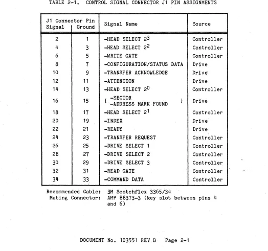
TABLE 2-1. CONTROL SIGNAL CONNECTOR J1 PIN ASSIGNMENTS
J1 Connector Pin
Signal Name Source
Signal Ground
2 1 -HEAD SELECT 23 Controller
4 3 -HEAD SELECT 22 Controller
6 5 -WRITE GATE Controller
8 7 -CONFIGURATION/STATUS DATA Drive 10 9 -TRANSFER ACKNOWLEDGE Dri
ve-12 11 -ATTENTION Drive
14 13 -HEAD SELECT 20 Controller
16 15 { -SECTOR
-ADDRESS MARK FOUND } Drive'
18 17 -HEAD SELECT 21 Controller
20 19 -INDEX Drive
22 21 -READY Drive
24 23 -TRANSFER REQUEST Controller
26 25 -DRIVE SELECT 1 Controller
28 27 -DRIVE SELECT 2 Controller
30 29 -DRIVE SELECT 3 Controller
32 31 -READ GATE Controller
34 33 -COMMAND DATA Controlle,r
Recommended Cable: 3M Scotchflex 3365/34
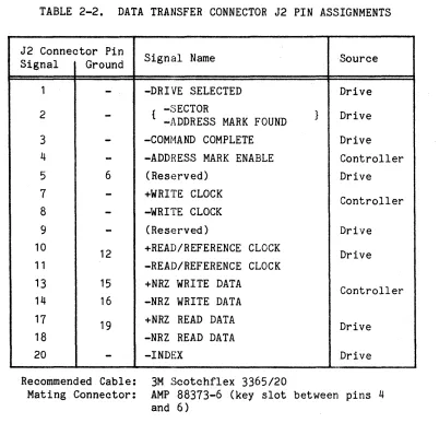
[image:14.612.53.577.282.773.2]TABLE 2-2. DATA TRANSFER CONNECTOR J2 PIN ASSIGNMENTS
J2 Connector Pin
Signal Name Source
Signal Ground
1
-
-DRIVE SELECTED Drive2
-
{ -SECTORMARK FOUND } Drive -ADDRESS
3
-
-COMMAND COMPLETE Drive4
-
-ADDRESS MARK ENABLE Controller5 6 (Reserved) Drive
7
-
+WRITE CLOCKController
8
-
-WRITE CLOCK9
-
(Reserved) Drive10
12 +READ/REFERENCE CLOCK Drive
11 -READ/REFERENCE CLOCK
13 15 +NRZ WRITE DATA
Controller 14 16 -NRZ WRITE DATA
17
19 +NRZ READ DATA Drive
18 -NRZ READ DATA
20
-
-INDEX DriveRecommended Cable: 3M Scotchflex 3365/20
Mating Connector: AMP 88373-6 (key slot between pins 4 and 6)
Power is supplied to the drive via AMP MATE-N-LOK Connector J3; refer to Section 4 for power requirements. Voltages in Table 2-3 are +5%, measured at the dri ve' s power connector. Suggested wire si ze is 18 AWG (minimum) for all pins. Recommended mating connector is AMP 1-480424-0; recommended pins are AMP 350078-4.
TABLE 2-3. DC POWER CONNECTOR J3 PIN ASSIGNMENTS
[image:15.612.101.503.74.461.2]2.2 INTERFACE ELECTRICAL CHARACTERISTICS
Figure 2-1 summarizes the electrical characteristics of the signals at Control Signal Connector J1. These signals control the drive and transfer drive status to the host controller. The signals are low-true at the inter-face, high-true into drivers and out of receivers, and have the following logic levels:
-48 milliamps (maximum) True
False
=
0.0 VDC to 0.4 VDC @ I
=
= 2.5 VDC to 5.25 VDC @ I
=
+250 microamps (open collector)Interface Cable Length 10 feet (3 meters)
+5V
150 ohms
Driver: 7438
I
maximumI
(or equivalent) ... I - - - l .. ~Receiver: 74LS14 (or equivalent)
=
=
NOTE: Termination resistors for lines originating at the controll er are located in the 1 ast drive. Lines originating at the drive are terminated at the controller.
Figure 2-1. Control Signal Driver/Receiver Combination
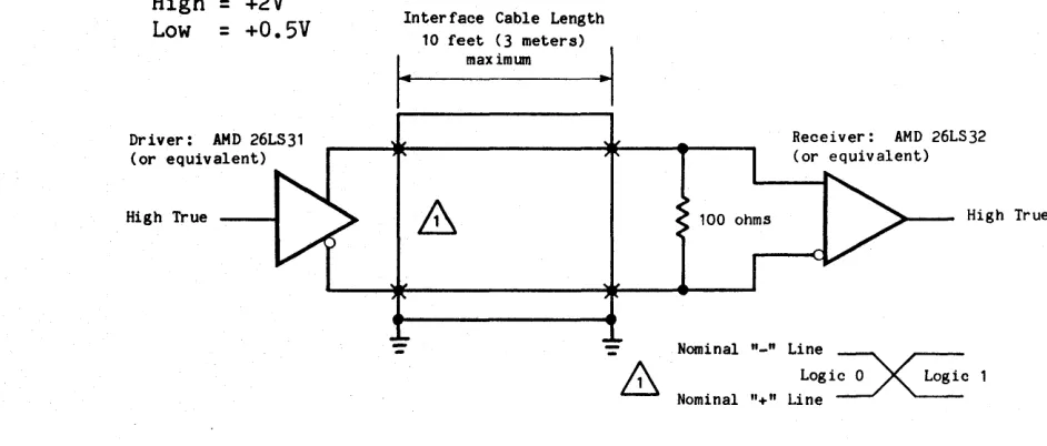
All interface data transfer signals are differential in nature. Figure 2-2 summarizes the electrical characteristics of those differential signals at Data Transfer Connector J2 (one TTL control signal and four TTL status signals are also provided at Connector J2). The signals are high true into drivers and out of receivers and have the following levels (EIA RS-422):
High
=
+2V Low=
+0.5VDriver: AMD 26LS31 (or equivalent)
High True
Inter face Cable Length 10 feet (3 meters)
·1
I-
maximumHigh True
Nominal "_" Line
LOgi~C
Nominal n+n Line
[image:16.612.39.555.103.741.2] [image:16.612.48.519.490.691.2]2.3 INTERFACE SIGNAL DESCRIPTIONS 2.3.1 Control Input Signals
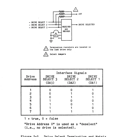
DRIVE SELECT 1 through DRIVE SELECT 3 (J1, Pins 26, 28, and 30)
Up to seven drives can be connected to one host controller/formatter. Drive Select 1, Drive Select 2, and Drive Select 3 carry the binary-coded address of the drive to be selected. The address of the drive is set with drive-selection jumpers DA1, DA2, and DA3 as a binary combina-tion. When the address is decoded and the decoded value matches the value specified by the three drive-selection jumpers, that drive is enabled to receive commands and transmit status. Drive Select 1 is the least significant bit •
... DRIVE SELECT 1 --+-1-+-1 - DRIVE SELECT 2 --~-1
- DRIVE SELECT 3 - -... -1
DRIVE SELECTED
1\ Termination resistors are located in
~ the last drive only
&
Select JumpersInterface Signals
Drive DRIVE DRIVE DRIVE
Address SELECT 3 SELECT 2 SELECT 1 . (DA3) (DA2) (DA1)
1 0 0 1
2 0 1 0
3 0 1 1
4 1 0 0
5 1 0 1
6 1 1 0
7 1 1 1
1
=
true, 0=
false"Drive Address 0" is used as a "deselect" (i.e., no drive is selected).
[image:17.612.87.488.240.696.2]2.3.1 Control Input Signals (continued)
HEAD SELECT 20 through HEAD SELECT 23 (J1, Pins 14, 18, 4, and 2)
These four head-select lines furnish a binary-coded address which, when decoded, selects the corresponding data head. The four lines prov ide for the selection of up to sixteen data heads (addressed 0 through 15). A 150-ohm resistor pack allows for 1 ine termination. For 1350-series drives, the maximum number of data heads is eight. The heads are ad-dressed 0 through
7
(depending on the model) in a binary-coded sequence where Head Select 20 is the least significant bit. If all four Head Select lines are inactive, Head ~ is selected. An attempt to write to a head with an address greater than any contained in the drive will result in a write fault.WRITE GATE (J1, Pin 6)
When the Write Gate signal is active, (i.e., low) data may be written to the disk. The high-to-low transition of this signal creates a write splice and initiates the writing of the Data PLO Sync field by the drive; refer to Section 5. When formatting, the Write Gate signal should be deactivated for two bit times minimum between the address area and the data area to identify to the drive the beginning of the Data PLO Sync field. This line is protected from terminator power loss by imple-mentation of the circuit as shown in Figure 2-4.
+5V
150 ohms
&
&
3.9K ohmsWRITE GATE
/\. Part of the termination resistor pack in the last drive i l l of the daisy chain.
&.
Permanently located in the drive.Figure 2-4. Write Gate Termination READ GATE (J1, Pin 32)
2.3.1 Control Input Signals (continued) TRANSFER REQUEST (J1, Pin 2~)
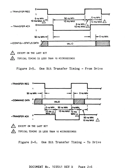
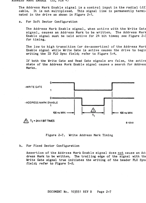
The Transfer Request signal functions as a "handshake" signal that is used in conjunction with the Transfer Acknowledge signal during Command and Configuration/Status transfers; see Figures 2-5 and 2-6 for timing. Typical timing for the complete 17-bit transfer is less than 200 micro-seconds.
- TRANSFER REO
:----~---~I
~
o MIN
I
so ns MINI
~
nsMI~
I
10mS~AX&~
I-
10msMAX •~,omSMAX&
o
0 ns MIN / A ~ f- TRANSFER ACK - - - . , 10 ms MAX&I '
a . . . - . I __~I
so
ns M1N-i---I
1-
0 ns MIN-CONFIG/-STATUS OATA 1 ~,.~r---VA-L-ID---""'~~~""'''''
~ EXCEPT ON THE LAST BIT
&
TYPICAL TIMING IS LESS THAN 10 HICROSECONDSFigure 2-5. One Bit Transfer Timing - From Drive
-TRANSFER REO 0
I
I
,
l-
~
I,
SOnsMIN
I
I
OnSMI~I
-COMMAND DATA ~ ~ VALID
~
~
-TRANSFER ACK o
~ EXCEPT ON THE LAST BIT
~ TYPICAL TIMING IS LESS THAN 10 MICROSECONDS
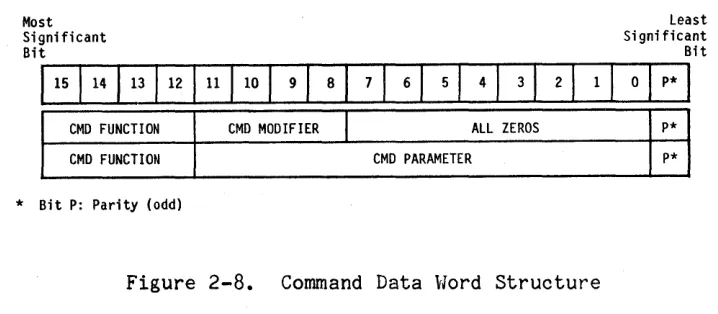
[image:19.612.94.558.187.758.2]2.3.1 Control Input Signals (continued) ADDRESS MARK ENABLE (J2, Pin 4)
The Address Mark Enable signal is a control input in the radial (J2) cable. It is not multiplexed. This signal line is permanently termi-nated in the drive as shown in Figure 2-1.
a. For Soft Sector Configuration
The Address Mark Enable signal, when active with the Write Gate signal, causes an Address Mark to be written. The Address Mark Enable signal must be held active for 24 bit times; see Figure 2-7 for timing.
The low to high transition (or de-assertion) of the Address Mark Enable signal while Write Gate is active causes the drive to begin writing the ID PLO Sync field; refer to Figure 5-4.
If both the Write Gate and Read Gate signals are false, the active state of the Address Mark Enable signal causes a search for Address Marks.
-WRITE GATE
0---1
I
I
O---~
-ADDRESS MARK ENABLE
J
I
1 100 ns MIN
I.
I
L
lOOns MIN.1
&
T1=
24±1 BIT TIMESE-123"()
Figure 2-7. Write Address Mark Timing
b. For Fixed Sector Configuration
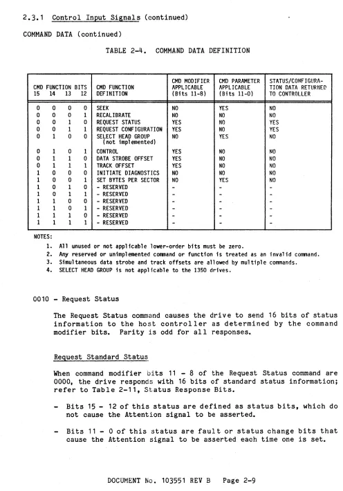
[image:20.612.52.543.105.789.2]2.3.1 Control Input Signals (continued) COMMAND DATA (J1, Pin 34)
When a command is sent to the drive, sixteen bits of serial data, plus parity, are presented on this line. Figure 2-8 shows the structure for the command data word.
Parity utilized in all commands is odd. The parity bit is a "1" when the number of 1 bits in a sixteen-bit command is even. As a result, the total number of 1 bits in a command, including parity, is always odd.
Most Least
Significant Significant
Bit Bit
115 114
1
13 /12In 1
101
91
8I
7I
6I
5I
4I
3I
2I
1I
0I
p*I
CMD FUNCTION CMD MODIFIER
I
ALL ZEROS p* CMD FUNCTION CMD PARAMETER P** Bit P: Parity (odd)
Figure 2-8. Command Data Hord Structure
Command Data is controlled by "handshake" protocol with the Transfer Request and Transfer Acknowledge signals; Figure 2-6 specifies the timing. Upon receipt of the serial data, the drive performs the func-tion specified by the bit configurafunc-tion. The most significant bit (MSB) is transmitted first. No communications should be attempted unless the Command Complete line is true. Command definitions associated with the various bit configurations are shown in Table 2-4.
Note that the Command Data line must be at a logic zero when not in use.
Command Codes (Table 2-4) 0000 - Seek
The Seek command causes the drive to seek to the cylinder indicated by bi ts
a -
11. A Seek command restores track and data strobe off-sets to zero.0001 - Recalibrate
[image:21.612.114.473.229.386.2]2.3.1 Control Input Signals (continued) COMMAND DATA (continued)
TABLE 2-4. COMMAND DATA DEFINITION
CMD MODIFIER CMD PARAMETER STATUS/CONFIGURA-CMD FUNCTION BITS CMD FUNCTION APPLICABLE APPLICABLE TION DATA RETURNED 15 14 13 12 DEFINITION (Bits 11-8) (Bi ts 11-0) TO CONTROLLER
0 0 0 0 SEEK NO YES NO
0 0 0 1 RECALIBRATE NO NO NO
0 0 1 0 REQUEST STATUS YES NO YES
0 0 1 1 REQUEST CONFIGURATION YES NO YES 0 1 0 0 SELECT HEAD GROUP NO YES NO
(not implemented)
0 1 0 1 CONTROL YES NO NO
0 1 1 0 DATA STROBE OFFSET YES NO NO
0 1 1 1 TRACK OFFSET YES NO NO
1 0 0 0 INITIATE DIAGNOSTICS NO NO NO
1 0 0 1 SET BYTES PER SECTOR NO YES NO
1 0 1 0 - RESERVED
-
-
-1 0 1 1 - RESERVED
-
-
-1 1 0 0 - RESERVED
-
-
-1 1 0 1 - RESERVED
-
--1 1 1 0 - RESERVED
-
-
-1 1 1 1 - RESERVED
-
-
-NOTES:
1. All unused or not applicable lower-order bits must be zero.
2. Any reserved or unimplemented command or function is treated as an invalid command. 3. Simultaneous data strobe and track offsets are allowed by multiple commands. 4. SELECT HEAD GROUP is not applicable to the 1350 drives.
0010 - Request Status
The Request Status command causes the drive to send 16 bits of status information to the host controller as determined by the command modifier bits. Parity is odd for all responses.
Request Standard Status
When command modifier bits 11 - 8 of the Request Status command are 0000, the drive responds with 16 bits of standard status information; refer to Table 2-11, Status Response Bits.
Bits 15 - 12 of this status are defined as status bits, which do not cause the Attention signal to be asserted.
[image:22.612.52.548.60.769.2]2.3.1 Control Input Signals (continued)
COMMAND DATA (continued)
Request Vendor Unique Status (command modifier 0001)
Vendor Unique Status consists of one word of status and is on 1 y val id if bit 2 of the Standard Status is a one.
This status is only intended to be utilized by trained field main-tenance personnel and is not intended to be interpreted by disk
controllers or operating systems. If this bit is detected, the
controller should attempt to reset Standard Status and reattempt the original function a minimum of three times prior to defining the drive as inoperative. After the last attempt, the Vendor Unique Status word should be read by the controller and sent back to the system for a print out of these codes which may then be uti 1 ized by the field maintenance personnel.
Command modifiers 0010 thru 1111 are not implemented.
0011 - Request Configuration
The Request Configuration command causes the drive to send 16 bits of
configuration data to the host controller. The parity util ized in
all configuration responses is odd. The specific drive configuration is specified by bits 11 - 8 of the command; see Table 2-5.
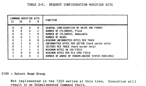
TABLE 2-5. REQUEST CONFIGURATION MODIFIER BITS
COMMAND MODIFIER BITS
FUNCTION
11 10 9 8
0 0 0 0 GENERAL CONFIGURATION OF DRIVE AND FORMAT
0 0 0 1 NUMBER OF CYLINDERS, Fixed
0 0 1 0 NUMBER OF CYLINDERS, Removable
0 0 1 1 NUMBER OF HEADS
0 1 0 0 ,MINIMUM UNFORMATTED BYTES PER TRACK
0 1 0 1 UNFORMATTED BYTES PER SECTOR (hard sector only)
0 1 1 0 SECTORS PER TRACK (hard sector only)
0 1 1 1 MINIMUM BYTES IN ISG FIELD
1 0 0 0 MINIMUM BYTES PER PLO SYNC FIELD
1 0 0 1 NUMBER OF WORDS OF VENDOR-UNIQUE STATUS AVAILABLE
0100 - Select Head Group
Not implemented in the 1350 series at this time. Execution will
[image:23.612.77.554.419.700.2]2.3.1 Control Input Signals (continued) COMMAND DATA (continued)
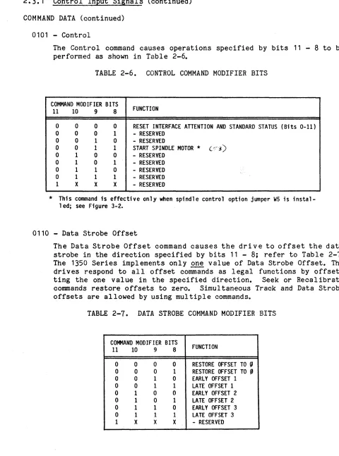
0101 - Control
The Control command causes operations specified by bits 11 - 8 to be performed as shown in Table 2-6.
TABLE 2-6. CONTROL COMMAND MODIFIER BITS
COMMAND MODIFIER BITS
FUNCTION
11 10 9 8
0 0 0 0 RESET INTERFACE ATTENTION AND STANDARD STATUS (Bits 0-11) 0 0 0 1 - RESERVED
0 0 1 0 - RESERVED
0 0 1 1 START SPINDLE MOTOR
*
(?,~.s)0 1 0 0 - RESERVED
0 1 0 1 - RESERVED
0 1 1 0 - RESERVED
0 1 1 1 - RESERVED 1 X X X - RESERVED
* This command is effective only when spindle control option jumper W5 is instal-l ed; see Figure 3-2.
0110 - Data Strobe Offset
The Data Strobe Offset command causes the drive to offset the data strobe in the direction specified by bits 11 - 8; refer to Table 2-7. The 1350 Series implements only ~ value of Data Strobe Offset. The drives respond to all offset commands as legal functions by offset-ting the one value in the specified direction. Seek or Recalibrate commands restore offsets to zero. Simultaneous Track and Data Strobe offsets are allowed by using multiple commands.
TABLE 2-7. DATA STROBE COMMAND MODIFIER BITS
COMMAND MODIFIER BITS
FUNCTION
11 10 9 8
0 0 0 0 RESTORE OFFSET TO ~
0 0 0 1 RESTORE OFFSET TO ~ 0 0 1 0 EARLY OFFSET 1
0 0 1 1 LATE OFFSET 1
[image:24.612.48.528.87.734.2]2.3.1 Control Input Signals (continued)
COMMAND DATA (continued)
0111 - Track Offset
The Track Offset command causes the drive to perform a track offset in the direction specified by bits 11 - 8; refer to Table 2-8. The 1350 Series implements only one offset value. The drives respond to all offset commands as legal functions by offsetting the one value in
the specified direction. Seek and Recalibrate commands restore the
offsets to zero. Simultaneous Track and Data Strobe offsets are
allowed by the use of mul tipl e commands.
TABLE 2-8. TRACK OFFSET COMMAND MODIFIER BITS
COMMAND MODIFIER BITS
FUNCTION
11 10 9 8
0 0 0 0 RESTORE OFFSET TO ~
0 0 0 1 RESTORE OFFSET TO ~
0 0 1 0 POSITIVE OFFSET 1
0 0 1 1 NEGATIVE OFFSET 1
0 1 0 0 POSITIVE OFFSET 2
0 1 0 1 NEGATIVE OFFSET 2
0 1 1 0 POSITIVE OFFSET 3
0 1 1 1 NEGATIVE OFFSET 3 1 X X X - RESERVED
1000 - Initiate Diagnostics
The Initiate Diagnostics command causes the drive to perform internal diagnostics. The Command Complete signal indicates the completion of
the diagnostics. The Attention signal, along with the Command
Com-plete signal, indicates that a fault was encountered and that status should be requested to determine a proper course of action. Extended fault information is made available in one word of Vendor Unique Status; see COMMAND DATA (Request Status, 0010).
1001 - Set Unformatted Bytes Per Sector
Note that this command is valid only if the drive is configured to be in the drive hard sector mode.
The Set Unformatted Bytes Per Sector command causes the drive to set the number of bytes per sector indicated by bits 11 - O. Sector size may be selected in one-byte increments, with a minimum of 82 bytes/
sector. If this command is not implemented by the host controller,
default sector sizes may be jumper selected by default sector option jumpers W2, W3, and \-/4; see Section 3.3.2.
[image:25.612.105.479.192.437.2]2.3.2 Control Output Signals
The output signals transfer drive status to the host controller. All J1 output signals are enabled/gated by their respective Drive Select line decode; J2 output control signals are ungated. Figure 2-1 shows the driver/ receiver combination used in 1350-series drives for control output signals. DRIVE SELECTED (J2, Pin 1)
Dri ve Selected is the status line that informs the host system of the selection status of the drive. This signal goes active when the drive is programmed as drive n (where n
=
1, 2, 3, 4, 5, 6, or 1) and the Drive Select lines at J1 are activated by the host system to produce a binary code equal to n.READY (J1, Pin 22)
When true, together with the Command Complete signal, the Ready signal i nd i cat es th at th e d r i v e is co nd i t ion ed to rea d, wr i t e, 0 r see k. Wh e n
this line is false, seeking or writing is inhibited.
CONFIGURATION/STATUS DATA (J1, Pin 8)
The drive presents serial configuration or status data on this line upon request from the host controller. The serial data is made available at the interface using Transfer Request and Transfer Acknowledge signals for the "handshake" protocol; see Figure 2-5. Once initiated, 16 bits plus parity are transmitted, MSB first; refer to Figure 2-9 for the data word structure, and see Figure 2-10 for a typical serial operation. The parity used is odd.
Most
Significant Bit
LI15 14
least Significant
13 12 11 10 9 8 7 6 5 4 3 2 1 0 p
jJ
[image:26.612.45.547.74.792.2]2.3.2 Control Output Signals (continued) CONFIGURATION/STATUS DATA (continued)
&.
o
r-
16 COMMANO BITS PLUS ONE PARITY arT...
--
...
16 INFORMATION arTS ~US ONE PARITY BIT
I
p
I
..
1---TRANSFER REO (FROM CONTROu.ER·
0 -__ ...
:-.1
~
100 ns~AX
VALlO
I f~1 _ _ _ _ _ _ _ _ _ _ _ _ _ r-~ ___________________________ ~
:1
&
" ! K1&
-ATTENTION
,F'AC::>M DRIve,
~---~
. . . . 1 14 t~Ons1
I I
I .
TRANSFERFR~
CONTROLLER-I-t--
TO DRivE&
COMMAND COMPLETE IS DEACTIVATED FOR ALL COMMANDS TO THE DRIVE.&
COMMAND COMPLrn IS AC'TlVATEO TO SIGNIFY COMPlE1lON Of EXECUTlON Of A COMMAND APPUCABLE FOR .t.L.L COMMANDS.&
COMMAND COMPLETE IS ACTIVATED TO SIGNIFY COMPLEllON Of THE REQUESTED~ CONFlGURATION/STAlVS TRANSFER.
~ APPLICAB~E F~ A.LL REOUEST STATUS AND CONFIGURATION COMMANOS.
IF AN ERR~ WAS ENCOUNTERED DURING THE CURRENT COMMAND. ATTENTION MUST BE ACTIVATED AT LEAST -.00 ,. BEFORE COMMAND COMPL.ETE IS ACTIVATED.
Figure 2-10. Typical Serial Operation(s)
1) Configuration Response Bits
In response to the Request Configuration (0011) command, 16 bits of configuration information are returned to the host controller.
[image:27.612.58.549.66.756.2]2.3.2 Control Output Signals (continued) CONFIGURATION/STATUS DATA (continued)
TABLE 2-9. GENERAL CONFIGURATION RESPONSE BITS
BIT
FUNCTION
POSITION VALUE
15 TAPE DRIVE 0
14 FORMAT SPEED TOLERANCE GAP REQUIRED 0
13 TRACK OFFSET OPTION AVAILABLE 1 12 DATA STROBE OFFSET OPTION AVAILABLE 1 11 ROTATIONAL SPEED TOLERANCE > 0.5~ 0 10 TRANSFER RATE > 10 MHz 0
9 TRANSFER RATE> 5 MHz < 10 MHz 1 8 TRANSFER RATE < 5 MHz 0
7 REMOVABLE CARTRIDGE DRIVE 0
6 FIXED DRIVE 1
5 SPINDLE MOTOR CONTROL OPTION IMPLEMENTED X Selectable 4 HEAD SWITCH TIME > 15 usec 0
3 RLL ENCODED (not MFM) 1
2 CONTROLLER SOFT SECTORED (ADR Mark) X } Se 1 ec tab 1 e
1 DRIVE HARD SECTORED (Sector Pulses) X
0 CONTROLLER HARD SECTORED (Byte Clock) 0
If command modifier bits (11 - 8) other than 0000 are used, the specific configuration data shown in Table 2-10 is returned for each Request Configuration command with those modifiers.
TABLE 2-10. SPECIFIC CONFIGURATION RESPONSE BITS
COMMAND MODIFIER BITS
CONFIGURATION RESPONSE
11 10 9 8
0 0 0 1 NUMBER OF CYLINDERS, Fixed
0 0 1 0 NUMBER OF CYLINDERS, Removable (zero)
0 0 1 1 NUMBER OF HEADS
BITS 15-8: Removable drive heads BITS 7-0: Fixed heads
0 1 0 0 MINIMUM UNFORMATTED BYTES PER TRACK
0 1 0 1 UNFORMATTED BYTES PER SECTOR (hard sector only)
0 1 1 0 SECTORS PER TRACK (drive hard sector only) BITS 15-8: Spare
BITS 7-0: Sectors per track
0 1 1 1 MINIMUM BYTES IN ISG'FIELD * BITS 15-8: ISG Bytes after Index BITS 7-0: Bytes per ISG 1 0 0 0 MINIMUM BYTES PER PLO SYNC FIELD
BITS 15-8: Spare
BITS 7-0: Bytes per PLO Sync Field
1 0 0 1 NUMBER OF WORDS OF VENDOR-UNIQUE STATUS AVAILABLE BITS 15-4: Spare
BITS 3-0: Number of vendor-unique status words
[image:28.612.45.536.44.792.2]2.3.2 Control Output Signals (continued) CONFIGURATION/STATUS DATA (continued)
2) Status Response Bits
In response to the Request Status (0010) command, 16 bits of status information are sent to the host controller; see Table 2-11. Bits 15 - 12 of the status are defined as state bits which do not cause the Attention signal to be asserted. Bits 11 - 0 are fault or status-change bits which cause the Attention signal to be asserted.
TABLE 2-11. STATUS RESPONSE BITS
BIT
POSITION FUNCTION
15 - RESERVED
14 REMOVABLE MEDIA NOT PRESENT 13 WRITE PROTECTED, Removable Media 12 WRITE PROTECTED, Fixed Media
-
- - - -
-
-
- -
-
- -
-
-- -
-
-
-
- -
-
- -
-
-
--
-
--
--
- -
-
-11 - RESERVED 10 - RESERVED
9 SPINDLE MOTOR STOPPED (1)
8 POWER-ON RESET CONDITIONS EXIST (2) 7 COMMAND DATA PARITY FAULT
6 INTERFACE FAULT
5 INVALID OR UNIMPLEMENTED COMMAND FAULT (3) 4 SEEK FAULT
3 WRITE GATE WITH TRACK OFFSET FAULT 2 VENDOR UNIQUE STATUS AVAILABLE 1 WRITE FAULT (4)
0 REMOVABLE MEDIA CHANGED
(1) Spindle Motor stopped due to previous command to stop, or drive is in Power-On Reset condition.
(2) Reconfiguration or Start Spindle Motor command may be required.
(3) This status is issued when a command is received which is invalid or has not been implemented.
(4) Conditions that can cause a Write Fault are:
a. Write current in a head without WRITE GATE active, or no write current with WRITE GATE active and the drive selected.
b. Multiple heads selected, no head selected, or improperly selected with WRITE GATE active.
c. WRITE GATE active to a write-protected drive.
[image:29.612.57.522.130.761.2]2.3.2 Control Output Signals (continued) TRANSFER ACKNOWLEDGE (J1, Pin 10)
The Transfer Acknowledge signal functions as a "handshake" signal with the Transfer Request signal during Command and Configuration/Status transfers; refer to Figures 2-5 and 2-6.
ATTENTION (J1, Pin 12)
Note that the Attention signal is asserted when the drive wants the host controller to request its standard status. Generally this is a result of a faul t cond i tion or a change of status. Wri ting is inhi b i ted when Attention is asserted. The Attention signal is deactivated by Reset Interface Attention; see Section 2.3.1, COMMAND DATA (Control, 0101).
INDEX (J1, Pin 20; and J2, Pin 20)
A Index pulse is generated once per disk revolution (nominally every 16.7 milliseconds) to indicate the beginning of a track. This signal is normally high and makes the transition to logical true to indicate Index; see Figure 2-11. Only the transition from high to low (the leading edge) is valid. This signal is available on Jl (gated) and on J2 (ungated).
1
.. - - - 16.7 msec
o--.--.U
-INDEX
-I
I 0.5,,5 MINt--500,.5 MAX
Figure 2-11. Index Pulse Timing
SECTOR or ADDRESS MARK FOUND (J1, Pin 16; and J2, Pin 2)
2.3.2 Control Output Signals (continued) 1) Sector (Drive Hard Sector)
This optional interface signal indicates the start of a sector. No short sectors are generated. The leading edge of the sector pulses is the only edge that is accurately controlled. The Index pulse indicates sector zero; see Figure 2-12.
-INDEX
-SECTOR
---I
t--
0.5 lAS MINI
I
50) lAS tAAXo---.u
I
!
--j
r~~
O----~LJ~~:~--~LJ
LAST
I
LASTI
SECTORI
SECTORSECTOR-1-+-SECTOR~ 0
+-
1Figure 2-12. Sector Pulse Timing
2) Address Mark Found (Controller Soft Sector)
This signal indicates the detection of the end of an Address Mark; see Figure 2-13 for timing.
-ADDRESS MARK ENABLE 0
-ADDRESS MARK FOUND 0
ADDRESS
J MARK PlO SYNC
I-t-
REFEFlENCE CLOCKS -:--_ _ _ _ _ _ _ _ _ - - , 8 MAX-READ GATE 0
&
T 1 • MtNIMUN TIME DETERMINED BY DRIVE MANUFACTURER&
LEADING EDGE INDICATES THE LOCATION OF THE END OF AN ADDRESS MARK. [image:31.612.76.564.29.777.2]2.3.2 Control Output Signals (continued) COMMAND COMPLETE (J2, Pin 3)
The Command Complete status line permits the host controller to monitor the drive's activity, without selecting the drive. The Command Complete signal goes false for the following reasons:
- A recalibration sequence is initiated (by drive logic) at power-on, if the read/write heads are not positioned over Track 0.
Upon receipt of the first Command Data bit.
The Command Complete signal remains false during the entire command sequence.
2.3.3 Data Transfer Signals
All data-transfer lines between the drive and the host system are differen-tial in nature and may not be multiplexed. Four pairs of balanced signals are used to transfer data: NRZ Write Data, NRZ Read Data, Write Clock, and Read/Reference Clock. Figure 2-2 shows the driver/receiver combination used for data-transfer signals.
NRZ WRITE DATA (J2, Pins 13 and 14)
The NRZ Write Data pair of signals defines the data to be written on the disk. The data is clocked by Write Clock; see Figure 2-14 for timing.
NRZ READ DATA (J2, Pins 17 and 18)
Read Data is transmitted to the host system via the NRZ Read Data signal pair. The data is clocked by the Read/Reference Clock signal; see Figure 2-14 for timing. These lines are held at a zero level until PLO sync has been obtained and the data is valid.
WRITE CLOCK (J2, Pins 1 and 8)
READ/REFERENCE CLOCK (J2, Pins 10 and 11)
The timing diagram shown in Figure 2-14 illustrates the sequence of events (with associated timing restrictions) for proper read/write oper-ation of the 1350-series drives. The Read/Reference Clock signal from the drive determines the data-transfer rate. The transition from Read Clock to Reference Clock is performed without "glitches," but up to two clock cycles may be missing. Read/Reference Clock is synchronized to spindle rotation.
,
-REFERENCE CLOCK
&
o
0.5 T '0.05 T
--..l
WRITE TIMING READ TIMING NOTES
&
&
&
&
&
&
NRZ WRITEDATA 0 _ _ _ 0 _ _ _ 0 _ _ _ _ _
WRITE CLOCK 0
o
o&1
0.5T 'Q.29T~
---..t-
T~
0.072T&
READ CLOCK
o
o
NRZ
READ
0---...
DATA
o
o
0 o-I
J...-
T± o.nALL TIMES IN ns MEASURED AT I/O CONNECTOR OF THE DRIVE T IS THE PERIOD OF THE CLOCK SIGNALS AND IS THE INVERSE OF THE REFERENCE OR READ CLOCK FREQUENCY.
1..-SIMILAR PERIOD SYMMETRY SHALL BE IN ± 4ns BETWEEN ANY TWO ADJACENT CYCLES DURING READING OR WRITING.
EXCEPT DURING A HEAD CHANGE OR PLO SYNCHRONIZATION THE CLOCK VARIANCES FOR SPINDLE SPEED AND CIRCUIT TOLERANCES SHALL NOT VARY MORE THAN -5.5~'O to +5.0% PHASE RELATIONSHIP BETWEEN REFERENCE CLOCK AND NRZ WRITE DATA OR WRITE CLOCK IS NOT DEFINED.
THE WRITE CLOCK MUST BE THE SAME FREOUENCY AS THE DRIVE SUPPLIED REFERENCE CLOCK (i.e. THE WRITE CLOCK IS THE CONTROLLER RECEIVED AND RETRANSMITIED DRIVE REFERENCE CLOCK)
REFERENCE CLOCK IS VALID WHEN READ GATE IS INACTIVE. READ CLOCK IS VALID WHEN READ GATE IS ACTIVE AND PLO SYNCHRONIZATION HAS BEEN ESTABLISHED.
SEE FIGURE 2-2 F<R IHINITION (F li AN) 1 ON THESE DIFFERENTIAL SI94AL LINES.
[image:33.612.49.528.201.719.2]2.4 READ, WRITE, AND FORMAT PARAMETERS
2.4.1 General Summary of Critical Read-Function Timing Parameters
Controller variations of the read timing are allowed if the following drive-dependent parameters are met:
• Read Initialization Time
A read operation may not be initiated until 15 microseconds following a head change.
• Read-Gate Timing
The Read Gate signal may not be enabled or true during a write-splice area. The Read Gate signal must be deactivated one bit time minimum before a write-splice area and may be enabled one bit time minimum after a write-splice area.
• Read Propagation Delay
Data read at the interface is delayed by up to nine bit times from the data recorded on the disk.
• Read Clock Timing
Read Clock and Read Data are valid within the number of PLO Sync field bytes specified by the drive configuration after Read Enable and a PLO Sync field is encountered. The Interface Read/Reference Clock line may contain no transitions for up to two Reference Clock periods for transi-tions between reference and read clocks. The transition period will also be one-half of a Reference Clock period minimum with no shortened pulse widths.
2.4.2 General Summary of Critical Write-Function Parameters
Controller timing variations in the record-update function are allowed if the following drive-dependent write (and interrelated read) timing para-meters are met:
• Read-to-Write Recovery Time
• Write Clock-to-Write Gate Timing
Write Clock must precede Write Gate by a minimum of two and a half Reference Clock periods.
• Write-Driver Plus Data-Encoder Turn-On from Write Gate
The write-driver plus data-encoder turn-on time (write-splice width) is between three and seven Reference Clock periods.
• Write-Driver Turn-Off from Write Gate
To account for data-encoding delays, the Write Gate signal must be held on for at least two byte times after the last bit of the information to be recorded.
• Write-to-React Recovery Time
The time lapse before Read Gate or Address Mark Enable signals can be activated after deactivating the Write Gate signal is ten microseconds.
• Head-Switching Time
The Write Gate signal must be deactivated at least one microsecond before a head change. Write Gate may not be activated until 15 microseconds after a head change or after the Command Complete signal is true.
• Reference Clocks Valid Time
The Read/Reference Clock lines will contain valid Reference Clocks within two Reference Clock periods after deactivation of the Read Gate signal. Pulse widths will not be shortened during the transition time, but clock transitions may not occur for up to two Reference Clock periods.
• Read Clocks Valid Time
The Read/Reference Clock line will contain valid Read clocks within two Clock periods after PLO synchronization is established. Pulse widths will not be shortened during the Reference Clock to Read Clock transition time, but missing clocks may occur for up to two clock periods.
• Write Propagation Delay
SECTION 3. INSTALLATION
3.1 PHYSICAL INTERFACE
The electrical interface between the 1350-series drive and the host system is accomplished via five connectors: J1, J2, J3, J4, and J5. The connec-tors and their recommended mating connecconnec-tors are described below.
3.2 POWER AND INTERFACE CABLES AND CONNECTORS
Figure 3-1 shows the locations of the power and interface connectors. Pin assignments for J1, J2, and J3 are listed in Section 2.1.
HDA Ground
Connector J 4 ~=:;:::;::=:;::;;==:::;========::::;:::::===;:::;:::=;::;=::::;,
Outer Frame Ground
Connector J5 --+I---~~
____ ---~--~r-Pin 1
Power Connector J3
Data Transfer Connector J2
I
I
Control Signal Connector Jl
Figure 3-1. Power and Interface Connections
The signal interface connection is made through connectors J1 and J2 on the Device Electronics board. The control cable interconnects the controller and J1; the data cable interconnects the controller and J2.
Control Signal Connector J1
J1 is a 34-pin board-edge connector on the Device Electronics board. The signals on this connector control the drive and transfer drive status to the host controller.
Recommended Cable: 3M Scotchflex 3365/34
Mating Connector: AMP 88373-3 (key slot between pins 4 and 6) Data Transfer Connector J2
J2 is a 20-pin board-edge connector on the Device Electronics board. The signals on this connector contain read or write data.
Recommended Cable: 3M Scotchflex 3365/20
[image:36.612.52.534.246.449.2]DC Power Connector
J3
J3 is a 4-pin, keyed AMP MATE-N-LOCK connector on the Motor Control board. This connector supplies DC power (+5V and +12V) to the drive. Mating Connector: AMP 1-480424-0
Pins: AMP 350078-4 Suggested Wire Size: 18 AWG
Ground Connectors J4 and J5
1/4-inch spade lugs J4 and J5 are provided for grounding; system char-acteristics determine the proper ground connection. J4 is located on the HDA, near the left-hand shock mount (as viewed from the rear of th~
drive). J5 is located on the Outer Frame near Power Connector J3. Mating Connector: AMP 62187-1 or equivalent
3.3 DRIVE OPTION SELECTION
3.3.1 Drive Addressing and Interface Termination
Figure 3-2 shows the locations of the three Drive Address jumpers (DA1, DA2, and DA3) for Drive Address selection (Drive Addresses 1 through 7) and Interface Terminator Pack RN1 on the Device Electronics board. The drive is configured for Drive Address 1 at the factory; see Table 3-1.
TABLE 3-1. DRIVE SELECT MATRIX
Drive Select Jumpers Address DA3 DA2 DA1
1 out out in
2 out in out
3 out in in
4 in out out
5 in out in
6 in in out
7 in in in
[image:37.612.74.404.452.640.2]The three Drive Select interface lines are decoded to select the correspond-ingly addressed drive to the host controller/formatter. In multiple-drive systems, each drive must have its own unique address.
Terminator Pack RN1 provides proper termination for the interface lines. When daisy-chaining multiple 1350 drives, the terminator is installed only in the last drive on the daisy chain.
D
J2
Pin 1
~!
}
DEFAULT SECTOR CONFIGURATIOtiru
Wl HARD/SOFT SECTORWS SPINDLE COtiTROL
0
J1
DAl
DA2} DRIVE SELECTION
DA3 Component Side
Figure 3-2. Option Jumpers and Interface Terminator
3.3.2 Spindle Control Option
Jumper W5 selects the spindle control option.
o
- When W5 is installed, the drive must wait for a Start Spindle command to start the spindle motor.
[image:38.612.50.540.194.585.2]3.3.3 Sectoring Options
Figure 3-2 shows the locations of the four jumpers (W1, W2, W3, and W4) associated with sector configuration options.
Jumper W1 selects hard or soft sectoring mode.
- When W1 is installed, the drive is configured to operate in the soft-sectored mode. Address mark generation and detection are enabled, and the Sector/Address Mark Found interface signal is used to report address mark found. Sector size is selected by the host controller.
- When W1 is not installed (the factory default configuration), the drive is configured to operate in the hard-sectored mode. The Sector/Address Mark Found interface signal is used to transmit sector pulses to the host controller.
Sector pulses are derived from the servo disk. The number of sector pulses generated is equal to:
INT [ 20,832 ]
n
Where 20,832
=
byte clock derived from servo disk INT=
integer part ofn
=
the number of bytes/sector (82 minimum)The number of bytes/sector may be specified using the Set Bytes Per Sector command or by selecting a default sector configuration with option jumpers W2, W3, and W4. Sector configurations may be selected as shown in Table 3-2. Other combinations of sector numbers and bytes per sector are available; contact Micropolis Product Support for details.
TABLE 3-2. DEFAULT HARD SECTOR CONFIGURATION WITH JUMPER OPTIONS
SECTORS BYTES/SECTOR JUMPERS
Formatted Unformatted W4 W3 W2
35 512 595 out out out
63 256 330 out out in
19 1024 1096 out in out
9 2048 2314 out in in
5 4096 4166 in out out
32 512 651 in out in
64 256 325 in in out
3.4 DAISY-CHAINING THE 1350 DRIVE
Up to seven 1350-series drives may be connected to a single host controller/ formatter. Control signals at J1 are transmitted via standard, daisy-chain interconnection. Data signals at J2 are transmitted via radially connected data-transfer lines. Figure 3-3 shows the connections for a system config-uration using four dri ves.
HOST
CONTROL
...
~J,
..,
...
~
...
J2DRIVE "
r-t:
J3J~/J5
tt
CONTROLLER
-
J1L..
-
"- J2 DRIVE '24~ J3
J4/J5
'r
.r- J1 L..
-
J2L.. DRIVE '3
r--C
J3DATA J4/J5
M
Y
~ ~
~
~
-
J1I
I
~
....
RN1 •""'"
-
J2~
....
DRIVE , ..~ J3
J4/J5
L~ DC VOLTAGES
GROUND
• Interface Terminator RN1 is installed only in the last physical drive in the control chain.
[image:40.612.48.559.86.748.2]3.5 DIMENSIONS AND MOUNTING
The 1350 Series uses industry-standard mounting for 5 1/4-inch Winchester disk drives (the same as for 5 1/4-inch flexible disk drives). Figure 3-4 shows the mounting hole locations. The length of the mounting screws must be such that the screws do not penetrate the mounting holes by more than 0.25 inch. Maximum torque applied to the screws must not exceed 10 in-lbs. Recommended orientation is vertical on either side, or horizontal with the Device Electronics board down; other mounting orientations may be used pro v ided the ambient air temperature around the dri ve is kept at or be low 500C (1220F).
Inasmuch as the drive frame acts as a heat sink to dissipate heat from the unit, the enclosure and mounting structure should be designed to allow natural convection of heat around the HDA and outer frame. If the enclosure is small or if natural convection is restricted, a fan may be required.
3.38 !.ot
--.-O.86!.005
...L-.07 +.01 I I
- 0.185!.005
--!
L
~:~5--i. i----3.12!.005~
""",_1---8.00
~::g---o~L;:~
.1.
I
3.12 !.005---1
Figure 3-4. Dimensions and Mounting
DIMENSIONS IN INCHES
MOUNTING HOLES: 4 ON BOTTOM, 2 PER SIDE, *6·32UNC-2B
[image:41.612.51.544.302.762.2]SECTION 4. POWER REQUIREMENTS
4.1 POWER SUPPLY REQUIREMENTS
DC vol tage and current requi rements for the 1350 Series are shown be low. Voltages may be applied to the drive in any sequence during power-up. Volt-age verification must be performed at the drive connector. The rise time of the +5V must be less than 50 milliseconds for proper operation of the power-on reset circuits. Figure 4-1 shows the current profile for the +12V.
TABLE 4-1. DC POWER REQUIREMENTS
Voltage Avg. Start-up Peak Avg. Idle Peak Avg. Seeking Peak (1) (maximum) Ripple
+5V .:!:5~ 2~
maximum: (2) 2.0A 2.0A 2.0A 2.0A 2.DA 2.0A
+12V +5~ (3) 2%
typical: (4) 4.25A 4.25A 1.80A 1.g0A 2.25A 3.10A maximum: (2) 4.35A 4.35A 2.00A 2.10A 2.45A 3.30A
(1) These val ues are for l/3-stroke seeks with an 8-mill isecond id 1 e period between seeks to simulate a typical system environment. (2) Maximum values to be considered for power supply design and system
integration.
(3) +5%, -10~ tolerance during start-up. (4) Typically measured values.
DC POWER PIN ASSIGNMENTS (Connector J3)
Pin Voltage Pin Voltage
1 +12 VDC 3 +5 RETURN 2 +12 RETURN 4 +5 VDC
5 Amps
4.25A
3.1A
3
1.9A
2 ~ _ _ _ _ _ _ _ _ -J'I I
I t i 1100 usee I
I r (typ) I
I I
o
111 .sec (typ)
I S t a r t U p t : D r i v e Ready
-(12 sec typ) (Idling)
Full Stroke Seek (typ)
[image:42.612.48.532.197.747.2]SECTION 5. DATA ORGANIZATION
5.1 TRACK FORMAT
5.1.1 Fixed Sector Format
The record format on the disk is under control of the host controller. The Index and Sector pulses are available for use by the controller to indicate the beginning of a track and allow the controller to define the beginning of a sector. A suggested format for fixed data records is shown in Figure 5-1.
I
-INoEXl I SECTOR L.J
FIXED SECTOR "N' IDENTICAL SECTORS
'\
SECTOR
U
~t--I
-
ADDRESS AREA - - - -... 1 ... - - - - -OATA AREA ---IF!f--I.0
fA
&
&
/1
&& 11
/1
&
&
&
&£ 11
&
B¥TE AoR Bm DATA FORMAT
ISG PLO SYNC ADDRESS ADA PAD 2 WRITE PLO SYNC DATA PAD <> SPEED SYNC PATIERN RELD CHECK BVTES SPLICE SYNC PATTERN DATA CHECK BYTES TOLERANCE
00 00 , B¥TE BYTES 00 'B'fTE 00 'BYTE FIELD BYTES 00
/
~
CYLINDER CYLINDER HEAD SECTOR FLAG SlATUS t.IISS LSB
&.
THESE AREAS ARE EXAMPLES ONlY AN> MAY BE STROCTLRED TO SUIT INDI YIDUAL CUSTOMER REQUIREMENTS.&
Tt£ NUMBER a: CHECK BYTES IS USER DEFINED.&.
PlO SYNC FiElD AND ISG ARE REPORTED IN RESPONSE TO THE REQUEST CONFIGmATlON COMMANDS: - ISG IS 16 BYTES MINIMUM.- PLO SYNC IS 16 BYTES MINIMlJ4.
&
ALL BYTE tlM3ERS INO ICA TED ARE MIN IMlJ4S EXCEPT ADDRESS f IHD LENGTH.Ii:::.
NOT REQUIRED ON Tt£ 1350 SERIES; SEE PAGE 5-11.Figure 5-1. Fixed Sector Format
GAP 00
~
ISG
00
The format presented in Figure 5-1 consists of four functional areas: Intersector Gap
Address Area Data Area
Format Speed Tolerance Gap
[image:44.612.38.533.224.729.2]5.1.1 Fixed Sector Format (continued) Intersector Gap
The Intersector (ISG) Gap provides a separation between each sector. The minimum number of bytes in the Intersector Gap field is 16 (e.g., 4 bytes before Index and 12 bytes after Index). The Intersector Gap size is chosen to provide for:
Drive-required, write-to-read recovery time (minimum time between deassertion of Write Gate and assertion of Read Gate).
Drive-required head-switching time.
Host controller decision-making time between sectors. Other drive-required ISG times.
Variations in detecting Index. Address Area
The Address Area provides a positive indication of the track and sector locations. The Address Area is normally read by the host controller, and the address bytes verified prior to a Data Area read or write. The Address Area is normally only written by the controller during a format function, and thereafter only read to provide a positive indication of the sector location and establish the boundaries of the Data Area. The Address Area consists of the following bytes:
a. PLO Sync Field (11 bytes minimum)
PLO Sync Field bytes are required by the drive to allow the drive's read-data, phase-locked oscillator to become phase- and frequency-synchronized with the data bits recorded on the media. The host controller should send ~0s during this time. The number of bytes required may be determined by the Request Configuration command; see Section 2.3.1. The minimum number of bytes in the fie ld is 11.
b. Byte Sync Pattern (one byte minimum)
This byte establishes byte synchronization (i.e., the ability to partition the ensuing serial bit stream into meaningful information groupings, such as bytes) and indicates to the host controller the beginning of the address field information. It is recommended that the Byte Sync Pattern contain the hexadecimal pattern FE.
c. Address Field
5.1.1 Fixed Sector Format (continued)
d. ADR Check Bytes (Address Field Check Codes)
An appropriate error-detection mechanism is generated by the host controller and applied to the address for file-integrity purposes. These codes are written on the media during formatting. Data integrity is maintained by the controller recalculating and verify-ing the address-field check codes when the address field is read. ADR Check Bytes are user defined.
e. ADR Pad (two bytes minimum) - (Address Field Pad)
Data Area
The Address Field Pad bytes must be written by the host controller and are required by the drive to ensure proper recording and re-covery of the last bits of the address-field check codes. These pad bytes should be 00s.
The Data Area is used to record data fields. The contents of the data fields within the Data Area are specified by the host system. The remaining parts of the Data Area are specified and interpreted by the host controller to recover the data fields and ensure their integrity. The Data Area consists of:
a. Write Splice (one byte minimum)
This byte area is required by the drive to allow time for the write drivers to turn on and reach recording amplitude sufficient to ensure data recovery. Allowance should be made for this byte in the format, and the controller should send 00s during this time.
b. PLO Sync Bytes (11 bytes minimum)
These bytes are required when reading to allow the dri ve's phase-locked oscillator (PLO) to become phase- and frequency-synchronized with the data bits recorded on the media. The host controller should send a0s during these byte times. The number of bytes required may be determined by the Request Configuration command; see Section 2.3.1. The minimum number of bytes in the fie ld is 11.
c. Byte Sync Pattern (one byte minimum)
5.1.1 Fixed Sector Format (continued) d. Data Field
The Data Field contains the host system's data files.
e. Data Check Bytes (Data-Field Check Codes)
The Data Check bytes are generated by the host controller and are written on the media at the end of the Data Field. Data integrity is maintained by the controller recalculating and verifying the Data Field Check Codes or applying error correction algorithms, if applicable, when the Data Field is read.
The Data Check Field is user defined.
f. Data Pad (two bytes minimum) - (Data Field Pad)
The Data Field Pad bytes must be issued by the host controller. The pad is required by the drive to ensure proper recording and recovery of the last bits of the Data Field Check Codes. The controller should send 00s during these byte times.
Format Speed Tolerance Gap
The Format Speed Tolerance Gap is not required. This is due to the fact that the Read/Reference clock is synchronized to the rotation of the disk by the servo phase-locked loop. The number of clocks between sector or index pulses is fixed and independent of spindle speed varia-tion.
Fixed Sector Address Mark, Write Gate, and PLO Sync Format Timing
This timing is mainly to support drives that util ize unique encoding for PLO Sync fields (i.e., if Bit 3 in General Configuration Response is set to 1; refer to Table 2-9).
NOTE
The beginn