Spin switching in antiferromagnets using Néel-order spin-orbit
torques
P. Wadley and K. W. Edmonds†
School of Physics and Astronomy, University of Nottingham, University Park, Nottingham NG7 2RD, United Kingdom
Antiferromagnets offer considerable potential for electronic device applications. This article reviews recent demonstrations of spin manipulation in antiferromagnetic devices using applied
electrical currents. Due to spin-orbit coupling in environments with particular crystalline or structural symmetries, the electric current can induce an effective magnetic field with a sign that
alternates on the lengthscale of the unit cell. The staggered effective field provides an efficient mechanism for switching antiferromagnetic domains and moving antiferromagnetic domain walls, with writing speeds in the terahertz regime.
spintronics, antiferromagnetism, current-induced torques, magnetic domains
PACS:72.15.Gd, 75.50.Ee, 75.60.Ch, 85.75.-d
1. Introduction
The development of spintronic devices based on ferromagnetic (FM) metals has had a huge impact on information and communication technologies. Since the introduction of thin film magnetoresistive read heads in the mid-1990s, hard disk storage capacities have increased by several orders of magnitude. Ferromagnetic tunnel junctions form the bits of magnetic random access memories (MRAM), which offer advantages of nonvolatility, stability and high speed compared to competing semiconductor-based technologies. Antiferromagnetic (AF) materials, in which the local magnetic moment vectors of neighbouring atoms sum to zero, play a key, albeit passive, role in such devices: exchange coupling at the interface between FM and AF layers causes the FM layer to become stable against external magnetic fields, providing a fixed reference layer in a spin-valve structure. This important application has stimulated extensive research over the last two decades on exchange bias and other interface-induced phenomena at FM-AF interfaces[1].
AF materials have not yet found application as active components in spintronic devices, for two principal reasons. Firstly, the cancellation of neighbouring magnetic moments results in zero stray magnetic field, making their magnetic properties hard to measure. Secondly, AF materials are insensitive to external fields of typically several tesla, making them hard to control. However, neither the stray magnetic field nor the
Project supported by EPSRC (grant EP/P019749/1). P.W. acknowledges support from the Royal Society through
a University Research Fellowship.
sensitivity of external magnetic fields of FM layers are used in modern MRAM devices: information is read electrically using tunnel magnetoresistance, and electrical current-induced spin torques provide the writing mechanism. Therefore, these historic advantages of FM materials actually become a hindrance in MRAM, as the stray fields must be compensated to prevent unwanted cross-talk between neighbouring magnetic elements. It has been demonstrated that large tunnelling anisotropic magnetoresistance can be observed in tunnel junctions with an AF layer as the active element[2], providing an important proof of the principle that AF materials can provide the required electrical readout signals in a memory device. The recent demonstrations of electrical control of AF order [3-12], described in detail in the present review article, firmly establish the prospects for fully readable and writable AF devices.
Antiferromagnets offer a further important advantage over ferromagnets for spintronic device applications, in terms of the speed of operation. The limiting timescale for writing the magnetization state is set by the magnetic resonance frequency which is of the order of GHz in FM materials. On the other hand, the resonance frequency in AF materials is enhanced by the strong antiparallel coupling of neighbouring moments, and is typically in the THz range [13]. Hence, rapid reorientation of AF moments on a timescale of a few picoseconds is possible[14].
This article presents a focussed review of recent demonstrations of electrical switching in AF thin films using current-induced spin-orbit torques. For wider reviews of the rapidly developing field of AF spintronics, including spin transport, dynamical properties, opto-spintronics and topological effects, the reader is referred to the recent focus issue of Nature Physics[15]and other recent extensive reviews[16,17]. In the present review, Section 2 gives a brief overview of current-induced torques that arise in due to spin-orbit coupling in FM and AF materials. Section 3 describes the structure and properties of CuMnAs, a material which offers favourable characteristics for utilization in AF memory devices. This has been the focus of several recent studies of current-induced switching of AF order, including the first direct experimental observations[3], as well as high speed (up to THz) switching [6], as described in section 4. Section 5 collects together related studies in other material systems, particularly Mn2Au and Pt/NiO. A summary and outlook is given in section 6.
2. Spin-orbit torques in ferromagnets and antiferromagnets
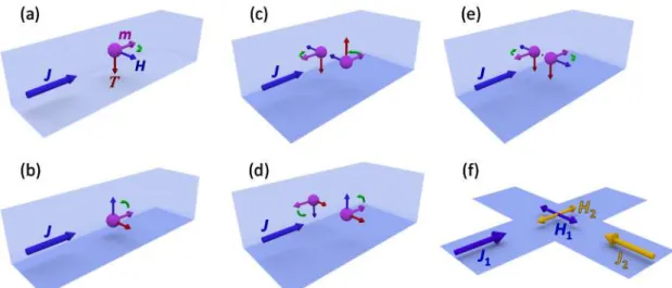
In systems with broken inversion symmetry, due to spin-orbit coupling the carrier momentum is correlated with the spin angular momentum; carriers propagating in opposite directions through the crystal lattice will have opposite direction of spin polarization. Hence, an electric current can induce a non-equilibrium spin polarization which, in a magnetic material, can induce a torque on the local magnetic moments. As illustrated in Fig. 1(a) and Fig. 1(b), this spin-orbit torque (SOT) can have two distinct components: a component with the form of a current-induced effective magnetic field (field-like torque),
wheremis the local magnetic moment, andis the current-induced spin polarization; and a component with the same form as the phenomenological damping term of the Landau-Lifschitz-Gilbert equation describing magnetization dynamics (damping-like torque):
DL~m(m). (2)
The inversion asymmetry giving rise to the non-equilibrium spin polarization can be either due to the bulk crystal structure (Dresselhaus effect)[18,19], or can be due to the built-in internal electric field at the surfaces or interfaces of materials, such as in heavy metal / FM bilayers (Rashba effect) [20,21]. In such structures, including Pt/Co and Ta/CoFeB, the part of the current flowing through the heavy metal layer induces a transverse spin current due to the spin Hall effect, and its absorption by the FM produces a damping-like torque[22]. It has been shown that the damping-like SOT due to either the Rashba effect or the spin Hall effect can induce magnetization switching in 3-terminal MRAM elements [20,23,24]. However, to ensure deterministic switching into a fixed direction determined by the current, either an external magnetic field or some other mechanism to break the in-plane symmetry is required in addition to the damping-like SOT[25-28].
In an antiferromagnet, a current-induced spin polarization due to inversion asymmetry can in principle act on the local magnetic moments through the same mechanisms as in ferromagnets. In the case of a field-like SOT in an AF material (Fig. 1(c)), the effective magnetic field competes against the inter-sublattice exchange coupling, with typical magnitude of several hundreds of teslas. Consequently, only a small canting of the AF-coupled moments can occur for realistic current densities. In contrast, the damping-like SOT acts with the same handedness on each sublattice (Fig. 1(d)), so can trigger a precession of the local magnetic moments while maintaining their antiferromagnetic configuration[29].
achieved by reversing the current polarity[33].
Current-induced motion of antiferromagnetic domain walls has been investigated both for damping-like torques [34]and Néel-order field-like torques [35]. A common feature of both studies is that the speed of the domain wall motion can be much larger in AFs than in FMs. In a FM material, the domain wall speed is limited by the so-called Walker breakdown, where the wall motion changes from a steady flow to an oscillatory behaviour associated with the precession of the wall magnetization [36]. In an AF material, the precession is opposed by the strong inter-sublattice exchange coupling, and the wall speed is limited only by the (much larger) spin wave velocity. Hence, speeds of several 10s of km/s are predicted, compared to limiting speeds of typically 10-100 m/s for FM walls[35]. The antiferromagnetic exchange coupling also results in a very small domain wall inertia, favouring current-induced domain wall motion for ultra-short (~ps) current pulses[35].
Fig. 1.Illustration of the current-induced effective magnetic fieldHand spin-orbit torqueacting on a magnetic momentm(a,b) or a pair of antiferromagnetically coupled moments (c-e). (a,c)
Field-like torque; (b,d) Damping-Field-like torque; (e) Néel-order field-Field-like torque for magnetic moments which are inversion partners about the point labelled by an orange sphere. For the field-like torques, the
effective field is along the direction given by the local current-induced spin polarization , while for the damping-like torques it is along the direction given by m . The green curved arrows indicate the direction of rotation of the magnetic moments. (f) Scheme for switching the AF
staggered magnetization between two orthogonal easy axes using the Néel-order fieldsH1andH2 induced by currentsJ1andJ2applied along orthogonal directions.
3. Properties of tetragonal CuMnAs films
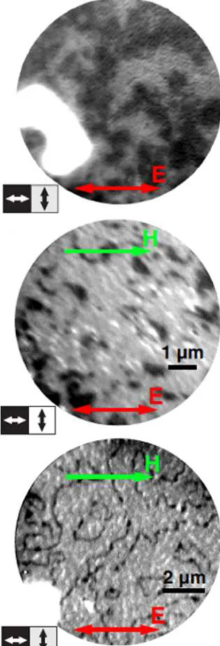
Fig. 2.(a) Unit cell structure and spin arrangement of tetragonal CuMnAs, with Mn (purple), Cu (blue) and As( orange) (from Ref. [40]). (b) Registry of the CuMnAs with a III-V semiconductor
substrate (from Ref. [40]). (c) X-ray 2scans (main figure) and reciprocal space maps (inset) of the CuMnAs(003) diffraction peak for layers on GaP and GaAs (from Ref. [40]). (d) Z-contrast scanning transmission electron microscopy image for the (100) plane of CuMnAs on GaP(001)
(from Ref. [3]). (e), (f) 10m field-of-view x-ray photoemission electron microscopy images of antiferromagnetic domains in (e) 80nm CuMnAs on GaAs(001) (adapted from Ref. [4]) and (f) 45nm CuMnAs on GaP(001) (adapted from Ref. [7]).
The stable bulk phase of CuMnAs has an orthorhombic structure [38,39], but the tetragonal phase can be stabilized by epitaxial growth on III-V semiconductor substrates[40]. Theabplane is lattice-matched to the substrate through a 45rotation as illustrated in Fig. 2(b). The ablattice parameter of 3.82Å is mismatched to GaP(001) along the diagonal by only 0.5%. X-ray diffraction (XRD) linescans and reciprocal space maps (Fig. 2(c)) indicate that the layer remains coherently strained on GaP(001) for thicknesses of several 10s of nm. In contrast, for growth on GaAs(001), strain relaxation is observed after only a few monolayers growth, and the resulting broadening of the reciprocal space map is described by a mosaic block model with lateral dimensions50nm. Z-resolved scanning transmission electron microscopy images (Fig. 2(d)) indicate a high degree of structural and chemical order of the films.
With increasing thickness, the uniaxial interface anisotropy becomes progressively less important, and the tetragonal anisotropy of the bulk crystal becomes dominant. However, the magnetic domain microstructure, measured using x-ray photoemission electron microscopy (XPEEM), is strongly dependent on the substrate. For CuMnAs films grown on GaAs(001), an inhomogeneous AF domain structure is observed (Fig. 2(e)), with no evident preference for a particular in-plane axis, and with length scales down to the spatial resolution of the measurement (50nm). This is likely to be related to a distribution of local strains in the film, consistent with the mosaic block structure revealed by XRD. For fully strained CuMnAs on GaP(001), a biaxial magnetic anisotropy is observed. The domains, with typical sizes of several micrometres, are found to have their spin axis aligned along one of the in-plane <110> axes of the CuMnAs film, and are separated by 90domain walls (Fig. 2(f)).
Recent theoretical studies have shown that the orthorhombic phase of CuMnAs also possesses a lattice symmetry favouring efficient switching by NSOT[43]. Moreover, the lower symmetry of this structure is predicted to favour a Dirac semimetallic band structure at the Fermi level [43,44], opening up the intriguing possibility of combining antiferromagnetic spintronics with topological Dirac physics. However, growth of orthorhombic CuMnAs thin films has not yet been reported, to our knowledge.
4. Néel-order spin-orbit torque in CuMnAs
The experimental geometry used in the first demonstration of current-induced switching in CuMnAs is shown in Fig. 3(a) [3]. Electrical current pulses are directed along the main axes of the 8-arm device, producing a current-induced Néel-order effective magnetic field perpendicular to the current. The diagonal arms allow electrical probing of the resistance anisotropy, which depends on the orientation of the antiferromagnetic spins. In the presence of either a FM or AF spin axis, the longitudinal and transverse components of the electrical resistance are given, respectively, by
R//=R0+R1cos(2) (3)
R=R1sin(2) (4)
Fig. 3.(a) Optical microscopy of an 8-arm CuMnAs device, and schematic of the electrical pulsing and measurement geometry. (b) Change in the transverse resistance after applying three successive
writing pulses of amplitudeJwrite= 4106Acm-2along the [100] axis (black arrow in (a) and black
points in (b)) and along the [010] axis (red arrow in (a) and red points in (b)). Adapted from Ref. [3].
The current-induced switching of AF domains into the NSOT effective field direction was confirmed by XPEEM imaging[4]. For an 80nm thick CuMnAs layer on GaAs(001), the AF moments were shown to be, on average, rotated to be perpendicular to the direction of the current pulse. A clear correlation was observed between the average spin orientation and the anisotropy of the electrical resistance, measured in-situ after each pulse. However, the observed switching was found to be inhomogeneous at the submicron scale. Small localized regions were found to consistently and reversibly switch with each current pulse, while other regions switch erratically or not at all. This is indicative of a stochastic process, highlighting the important role of thermal fluctuations and a distribution of domain wall pinning centres.
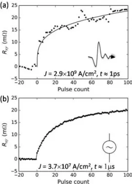
varying from 1ms to 250ps, and is ascribed to the multi-domain nature of the switching. The study was subsequently extended to the THz regime [6], where a remarkable consistency was observed between the effects of microsecond and picosecond pulses (Fig. 4).
Fig. 4.(a) Output signal of a 2m CuMnAs bit cell as a function of the number of applied picosecond pulses of amplitude 2.9109Acm-2. (b) Same as (a), but for microsecond pulses of amplitude 3107
Acm-2applied to a 3.5m CuMnAs bit cell. Adapted from Ref. [6].
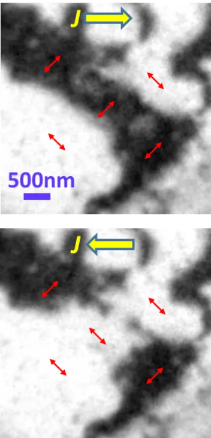
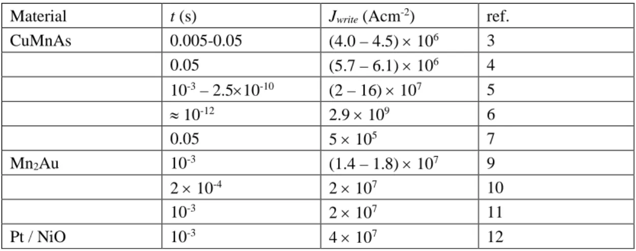
Fig. 5. XPEEM images showing current-induced writing of an antiferromagnetic domain in CuMnAs. The orientation of the staggered magnetization in the domain (red double-headed arrows)
is switched by 90when the polarity of the current pulse is reversed. Adapted from Ref. [7].
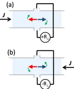
Current-induced switching of 180 domains was recently demonstrated using a novel phase-sensitive detection technique[8]. The technique relies on the fact that the current-induced local non-equilibrium spin polarization has opposite sign on the two magnetic sublattices. A current applied parallel to the uniaxial easy axis results in a transient rotation of the local moments towards the direction of the Néel-order effective magnetic field (Fig. 6(a)). Switching the magnetic sublattices reverses the handedness of the rotation (Fig. 6(b)). The resulting transient rotations can be detected using 2nd-harmonic transport measurements. The experiment, performed on a CuMnAs(10nm) / Pt(3nm) bilayer, indicated that a 180 spin reversal could be induced reproducibly by changing the polarity of the writing current pulse. It also indicated that the multi-level switching observed for 90rotation is not evident for 180switching, and also that the resulting domain configuration may be more stable.
J
J
J
Fig. 6.Experimental geometry used to detect the polarity of 180oantiferromagnetic domains. The
AF easy axis is oriented along the Hall bar. The staggered effective field due to an applied current
results in a transient rotation of the spin axis, in a direction that depends on the relative orientations of the sublattice magnetization and the current. The two rotation directions result in opposite sign
of the transverse resistanceR, detected using 2ndharmonic lock-in methods [8].
5. Current-induced switching in Mn2Au and Pt/NiO
Fig. 7. XPEEM images of the antiferromagnetic domain structure of a Mn2Au film in its initial state
(a), and after applying magnetic field pulses of 30T (b) and 50T (c) along one of the biaxial in-plane easy axes. Adapted from Ref. [47].
AF domain images obtained using XPEEM also indicate a substantial magnetocrystalline anisotropy in Mn2Au films [47]. Measurements of as-prepared Mn2Au(001) films revealed a biaxial magnetic anisotropy, with approximately equal populations of domains with spin oriented along the in-plane [110] and [11ത0] axes. After subjecting the films to external magnetic fields of between 30 and 50T along the [110] direction, domains were observed to be predominantly oriented along [11ത0],
THz spectroscopy measurements of Mn2Au films revealed a strong mode near 1THz, ascribed to a resonant in-plane oscillation of the AF coupled magnetic moments [48]. The absorption strength of the AF magnetic resonance is some 3 orders of magnitude larger than in insulating AF materials such as NiO, where the magnetic field component of the THz pulse drives the oscillation. In Mn2Au, due to the broken local inversion symmetry, the electric component of the pulse induces a Néel-order effective magnetic field, which can account for the observed strong AF magnetic resonance.
Current-induced switching behaviour was also demonstrated in bilayer films of Pt(5nm) / NiO(5nm) [12]. While the measurement geometry as well as the critical current densities were similar to the earlier studies of CuMnAs [3] and Mn2Au [9,10], there are crucial differences in the underlying mechanism. Firstly, the longitudinal and transverse resistance changes were ascribed to the spin Hall magnetoresistance effect in the Pt layer [49]. More importantly, the NiO film does not possess the broken sublattice inversion symmetry required for a Néel-order field-like torque. Instead, the switching is ascribed to the damping-like torque due non-equilibrium spin polarization generated in the Pt layer. The opposite sign of the resistance change in Pt/NiO compared to Mn2Au is consistent with this, and indicates that the AF-coupled local moments tend to switch into the axis of the current pulse. Some aspects of the observed switching behaviour are unclear, particularly the role of the AF domain microstructure in the quasiepitaxial NiO(001) film. However, the observed switching in a heavy-metal / AF bilayer points to a host of new possibilities for current-induced manipulation and high speed dynamics in AF thin films, without the requirement for a particular crystal symmetry.
Table 1 summarizes the range of writing current densities and pulse widths explored in CuMnAs, Mn2Au and Pt/NiO memory devices for which stable and reproducible switching of the AF order is reported.
Material t(s) Jwrite(Acm-2) ref.
CuMnAs 0.005-0.05 (4.0 – 4.5)106 3
0.05 (5.7 – 6.1)106 4
10-3– 2.510-10 (2 – 16)107 5
10-12 2.9109 6
0.05 5105 7
Mn2Au 10-3 (1.4 – 1.8)107 9
210-4 2107 10
10-3
2107 11
Pt / NiO 10-3 4107 12
Table 1.Current pulse width (t) and amplitude (Jwrite) used for switching of AF domains in CuMnAs,
6. Conclusion and perspectives
The recent rapid growth and development of antiferromagnetic spintronics is in large part associated with the discovery and demonstration of electrical switching in CuMnAs using NSOT. This offers an efficient and reversible method to control AF coupled spins, providing new possibilities for manipulating AF domains and domain walls and understanding their dynamical properties. Since then the demonstration of reproducible multi-level switching and response to terahertz pulses opens a pathway to applications in fields such as ultrafast processing and neuromorphic logic.
The demonstration of electrical current control in other AF material systems has broadened the material base for AF spintronics. Particularly the demonstration of switching in bilayer films, which are not limited by the same symmetry constraints, opens a new plethora of potential AF material systems.
Obstacles to application certainly exist and include the small size of the read-out signal using ohmic anisotropic magnetoresistance. The further development of AF tunneling anisotropic magnetoresistance structures would be of huge benefit. Another predicted property of some AF materials, including CuMnAs, could help to remedy this in a novel way. The predictions of the existence of a topological metal-insulator transition linked to the magnetic order[42]could provide a means of producing a large readout signal. As of yet the existence of this transition has not been demonstrated.
A further obstacle to application is the lack of understanding of what dictates the domain formation in these materials. The ability to tailor the domain size and anisotropies would allow one to design stable, single domain memory devices as well as to electrically manipulate individual AF domain walls. This would enable future spintronic devices utilizing AF domain wall motion induced by ultrafast current pulses.
References
1. Hellman F, Hoffman A, Tserkovnyak Y et al. 2017 Rev. Mod. Phys. 89 025006
2. Park B G, Wunderlich J, Marti X, Holy V, Kurosaki Y, Yamada M, Yamamoto H, Nishide A, Hayakawa J, Takahashi H, Shick A B and Jungwirth T 2011Nat. Mater.10347
3. Wadley P, Howells B, Zelezny Jet al.2016Science351587
4. Grzybowski M J, Wadley P, Edmonds K W, Beardsley R, Hills V, Campion R P, Gallagher B L, Chauhan J S, Novak V, Jungwirth T, Maccherozzi F and Dhesi S S 2017Phys. Rev. Lett.118
057701
5. Olejník K, Schuler V, Marti X, Novák V, Kašpar Z, Wadley P, Campion R P, Edmonds K W,
Gallagher B L, Garces J, Baumgartner M, Gambardella P and Jungwirth T 2017Nat. Commun.
815434
6. Olejnik K, Seifert T, Kašpar Z, Novák V, Wadley P, Campion R P, Baumgartner M, Gambardella P, Němec P, Wunderlich J, Sinova J, Kužel P, Müller M, Kampfrath T and Jungwirth T 2018
Science Adv.4eaar3566
Campion R P, Edmonds K W, Dhesi S S, Maccherozzi F, Novak V, Wunderlich J and
Jungwirth T 2018Nat. Nanotechnol.13362
8. Godinho J, Reichlova H, Kriegner D, Novak V, Olejnik K, Kaspar Z, Soban Z, Wadley P,
Campion R P, Otxoa R M, Roy P E, Zelezny J, Jungwirth T and Wunderlich J 2018 arXiv:
1806.02795 [cond-mat]
9. Bodnar S Yu,Šmejkal L, Turek I, Jungwirth T, Gomonay O, Sinova J, Sapozhnik A A, Elmers
H-J, Kläui M and Jourdan M 2018Nat. Commun.9348
10. Meinert M, Graulich D, and Matalla-Wagner T 2018Phys. Rev. Applied9, 064040
11. Zhou X F, Zhang J, Li F, Chen X Z, Shi G Y, Tan Y Z, Gu Y D, Saleem M S, Wu H Q, Pan F and Song C 2018Phys. Rev. Applied9054028
12. Chen X Z, Zarzuela R, Zhang J, Song C, Zhou X F, Shi G Y, Li F, Zhou H A, Jiang W J, Pan F
and Tserkovnyak Y 2018Phys. Rev. Lett.120207204 13. Kittel C 1951Phys. Rev.85565
14. Kimel A V, Kirilyuk A, Tsvetkov A, Pisarev R V and Rasing Th 2004Nature429850 15. Editorial 2018Nat. Phys.14199 and references therein.
16. Jungwirth T, Marti X, Wadley P and Wunderlich J 2016Nat. Nanotechnol.11231
17. Baltz V, Manchon A, Tsoi M, Moriyama T, Ono T and Tserkovnyak Y 2018Rev. Mod. Phys.90
015005
18. Chernyshov A, Overby M, Liu X, Furdyna J K, Lyanda-Geller Y and Rokhinson L P 2009Nat. Phys.5656
19. Ciccarelli C, Anderson L, Tshitoyan V, Ferguson A J, Gerhard F, Gould C, Molenkamp L W,
Gayles J,Železný J,Šmejkal L, Yuan Z, Sinova J, Freimuth F and Jungwirth T 2016Nat. Phys.
12855
20. Miron I M, Garello K, Gaudin G, Zermatten P-J, Costache M V, Auffret S, Bandiera S, Rodmacq B, Schuhl A and Gambardella P 2011Nature476189
21. Garello K, Miron I M, Avci C O, Freimuth F, Mokrousov Y, Blugel S, Auffret S, Boulle O,
Gaudin G and Gambardella P 2013Nat. Nanotechnol.8587
22. Liu L, Moriyama T, Ralph D C, and Buhrman R A 2011Phys. Rev. Lett.106036601 23. Liu L, Pai C-F, Li Y, Tseng H W, Ralph D C and Buhrman R A 2012Science336555 24. Fukami S, Anekawa T, Zhang C and Ohno H 2016Nat. Nanotechnol.11621
25. Yu G, Upadhyaya P, Fan Y, Alzate J G, Jiang W, Wong K L, Takei S, Bender S A, Chang L-T
and Jiang Y 2014Nat. Nanotechnol.9548
26. Oh Y-W, Baek S C, Kim Y, Lee H Y, Lee K D, Yang C D, Park E S, Lee K S, Kim K W, Go G,
Jeong J-R, Min B C, Lee H-W, Lee K-J and Park B-G 2016Nat. Nanotechnol.11878
27. Cai K, Yang M, Ju H, Wang S, Ji Y, Li B, Edmonds K W, Sheng Y, Zhang B, Zhang N, Liu S, Zheng H and Wang K Y 2017Nat. Mater.16712
28. Baek S C, Amin V P, O Y-W, Go G, Lee S-J, Lee G-H, Kim K-J, Stiles M D, Park B-G and Lee K-J 2018Nat. Mater.17509
29. Gomonay H V and Loktev V M 2010Phys. Rev. B81144427
30. Zhang X, Liu Q, Luo J-W, Freeman A J and Zunger A 2014Nat. Phys.10387
31. Zelezny J, Gao H, Vyborny K, Zemen J, Masek J, Manchon A, Wunderlich J, Sinova J and
Jungwirth T 2014Phys. Rev. Lett.113157201
32. Zelezny J, Gao H, Manchon A, Freimuth F, Mokrousov Y, Zemen J, Masek J, Sinova J and
33. Roy P E, Otxoa R M and Wunderlich J 2016Phys. Rev.B94014439
34. Shiino T, Oh S-H, Haney P M, Lee S-W, Go G, Park B-G and Lee K-J 2016Phys. Rev. Lett.
117087203
35. Gomonay O, Jungwirth T and Sinova J 2016Phys. Rev. Lett.117017202 36. Schryer N L and Walker L R 1974J. Appl. Phys.455406
37. Wadley P, Hills V, Shahedkhah M R, Edmonds K W, Campion R P, Novak V, Ouladdiaf B,
Khalyavin D, Langridge S, Saidl V, Nemec P, Rushforth A W, Gallagher B L, Dhesi S S, Maccherozzi F, Zelezny J and Jungwirth T 2015Sci. Rep.517079
38. Mundelein J and Schuster H U 1992Zeit. NaturforschungB47925
39. Máca F, Mašek J, Stelmakhovych O, Martí X, Reichlová H, Uhlířová K, Beran P, Wadley P, Novák V and Jungwirth T 2012J. Magn. Magn. Mater.3241606
40. Wadley P, Novak V, Campion R Pet al.2013Nat. Commun.42322
41. Saidl V, Nemec P, Wadley P, Hills V, Campion R P, Novak V, Edmonds K W, Maccherozzi F,
Dhesi S S, Gallagher B L, Trojanek F, Kunes J, Zelezny J, Maly P and Jungwirth T 2017Nat. Photon.1191
42. Wastlbauer G and Bland J A C 2005Adv. Phys.54137
43. Šmejkal L,Železný J, Sinova J and Jungwirth T 2017Phys. Rev. Lett.118106402 44. Tang P, Zhou Q, Xu G and Zhang S C 2016Nat. Phys.121100
45. Baumgartner M, Garello K, Mendil J, Avci CO, Grimaldi E, Murer C, Feng J, Gabureac M, Stamm C, Acremann Y, Finizio S, Wintz S, Raabe J and Gambardella P 2017Nat. Nanotechnol.
12980
46. Barthem V M T S, Colin C V, Mayaffre H, Julien M-H and Givord D 2013Nat. Commun.4
2892
47. Sapozhnik A A, Filianina M, Bodnar S Yu, Lamirand A, Mawass M-A, Skourski Y, Elmers H-J, Zabel H, Kläui M and Jourdan M 2018Phys. Rev.B97134429
48. Bhattacharjee N, Sapozhnik A A, Bodnar S Yu, Grigorev V Yu, Agustsson S Y, Cao J, Dominko
D, Obergfell M, Gomonay O, Sinova J, Kläui M, Elmers H-J, Jourdan M. and Demsar J 2018
Phys. Rev. Lett.120237201