This paper is a postprint of a paper submitted to and accepted for publication in IET Power Electronics
and is subject to Institution of Engineering and Technology Copyright. The copy of record is available at
IET Digital Library.
Z-Source Matrix Rectifier
Liu Hongchen1, Ji Yuliang1, Zhao Dan1, Pat wheeler2, Fan Guolei1
(1. School of Electrical Engineering and Automation, Harbin Institute of Technology, Harbin 150001, China)
(2. Department of Electrical and Electronics Engineering, University of Nottingham, Nottingham NG7 2RD, UK)
Abstract—This paper presents a novel Z-source matrix rectifier(ZSMR). To
overcome the inherent disadvantage that the voltage transfer ratio for traditional matrix rectifier cannot be more than 0.866, a Z-source network has been combined with the matrix rectifier. The proposed rectifier realizes a voltage-boost function and the Z-source network also serves as power storage and guarantees double filtration grade at the output of the rectifier. The open-circuit zero state is required to obtain the voltage-boost function and ensure the output angle of the current vector to be invariant to obtain the expected power factor. In addition, to widely extend the voltage transfer ratio of the proposed rectifier, this paper presents the switched-inductor matrix rectifier(SL-ZSMR) and tapped-inductor matrix rectifier(TL-ZSMR). The corresponding circuit topologies, control strategies and operating principles are introduced. Both simulation and experiment results are shown to verify the theoretical analysis.
Index Terms—Z-source matrix rectifier, voltage-boost function, voltage transfer
I. INTRODUCTION
The matrix rectifier (MR) originated from conventional matrix converter (MC) is a new type rectifier. Since the MR is the front-end rectification stage for indirect matrix converters, MRs and MCs share some same advantages such as input current with low harmonic content [1,8], controllable input power factor [2] and bidirectional energy flow [3]. The circuit has some potential applications and has recent attention in the field of power electronics [4]-[10]. For the high voltage ac-ac applications, the Z-source matrix converter is presented and researched such as the modulation strategies [11] and motor drives [12].
Similarly, the MR has some disadvantages that have restricted applications in the high voltage transfer ratio circumstance such as wind energy system [13] and electric vehicle charging system [14]. Since the Z-source network of the Z-source matrix rectifier presented by [15-18] serves as the filter at the dc side and does not play a voltage-boost role, the Z-source matrix rectifier presented by [15-18] is a voltage-buck ac-dc matrix rectifier, which does not satisfy the need for higher voltage transfer ratios. So, this paper presents a novel Z-source matrix rectifier (ZSMR) by improving the switch position, the switch count and the modulation scheme to realize the voltage-boost function.
topologies with higher boost ability, reduced device voltage stress and improved the output quality are proposed.
The ZSMR can be constructed by putting a Z-source network between a matrix converter and the output filter, in which the position of Z-source network in ZSMR is different from that of a Z-source network in [19-24]. Not only does ZSMR reserve the original advantages of the MR but also it realizes the voltage-boost feature. At the same time, the Z-source network also serves as energy storage component and guarantees double filtration grade at the output of the ZSMR.
To improve the relationship between boost factor and the modulation index of the ZSMR, this paper propose to replace the Z-source inductor cell with a switched-inductor cell or a tapped-inductor cell. The resulting structures of ZSMR, SL-ZSMR and TL-ZSMR are similar to the Z-source inverters in [19, 20, 25]. The TL-ZSMR is more compact with its turn ratio freely adjustable to produce the desired voltage gain when compared to the ZSMR and SL-ZSMR.
II. MODULATION STRATEGY AND EXPERIMENTAL PRINCIPLE OF
PROPOSED MATRIX RECTIFIERS
β 1 2 3 4 5 6
I6(Sap,Sbn) I1(Sap,Scn) I2(Sbp,Scn)
I3(Sbp,San)
I4(Scp,San)
I5(Scp,Sbn) I7(Sap,San) I8(Sbp,Sbn) I9(Scp,Scn)
7
I
9
I I8
I v I u Iref I u d uI v d v θip I0 d0
(a) (b)
Fig.1.(a) Current space vector.(b) Current vector synthesis.
As shown in Fig.1(b), the input current vector at any direction and amplitude can be synthesized by the two nearest adjacent current vectors (Ii and Ii+1, i=1,…6) and one
of the three zero vectors(I7 , I8, or I9 when both of the upper and lower switches are
short together). According to the current space vector synthesis theory, the reference vector can be expressed as follows:
Iref d Iu u d Iv vd I0 0 (1)
u
d , dv and d0 can be written:
0 0
2
sin( ) sin( ) sin( )
3 3 3
3 2
sin sin sin 3
1 ref
u im
u i i i
s u dc
ref
v im
v i i i
s v dc
u v s
I
T I
d m
T I I
I
T I
d m
T I I
T
d d d
T
(2)
Where Tu is the operation interval of the starting vector, and Tv is the operation interval of the ending vector in the sector. i is the angle between the reference
vector and the starting vector, m( im dc
I m
I
) is the modulation index and its range is
c o s ( / 6 ) c o s ( )
s i n ( / 6 ) c o s ( 2 / 3 ) s i n c o s ( 2 / 3 )
a u v i i
r e f b u d c i d c d c i
c v i i
i d d m t
I i d I m I m I t
i d m t
(3)
According to the equation (3), it is obvious that input reference current changes as the balanced three-phase sine law.
The above description is the modulation method used for traditional MRs, from which we can see that the traditional MR is a voltage-buck rectifier. So, to obtain the higher voltage-boost ratio, the modulation strategy for MRs should be modified. This paper introduces an extra open-circuit zero state forbidden in the matrix rectifier into the traditional current space vector control strategy.
An open-circuit zero state corresponds to the additional zero state different from traditional zero states produced by the shoot-though state of top and bottom arms (I7,
I8, or I9). The open-circuit zero state is the tenth switching state (I10) where the switch
S1 isturned on and all the switching devices of the MR should be turned off to ensure
the energy to flow from the capacitors to the inductors. The open-circuit zero state can solve the output open-circuit problem, which destroys the switch devices in a classical MR, and gives the Z-source inductor and inductive load current to a conduction path. The open-circuit zero state is similar to the shoot-though state in [17-23], and the non-open-circuit zero state is similar to nonshoot-though state.
To combine open-circuit zero state and keep the active states of the matrix rectifier unchanged, this paper proposes turning some of the short zero states(I7 , I8, or I9) into
zero state, but also ensure the angle of the output current vector to be invariant to obtain the expected power factor.
ap S
bp S
cp S
an
S
bn
S
cn
S
1
2
t 2
2 t
10
t t22 2t1
open - circuit zero state
L
C
O Ua
Ub
Uc L
s
Cf
Input filter Matrix rectifier
L
o
ad
Signal processing circuit
Output filter
Drive circuit
DSP+CPLD
A
u
x
ili
ar
y
p
o
w
er
Synchronous transformer
Z
-s
o
u
rc
e
Fig.2. (a) open-circuit zero state inserted into tradition zero.(b) the system structure for the experimental ZSMR.
As shown in Fig.2(b), the ZSMR mainly consists of six parts: three-phase power, input filter, matrix rectifier, Z-source network, output filter and load. ZSMR is connected to the input voltage through the synchronous transformer. The measured input voltage is processed to realize the pass-zero comparison and voltage transform.
To realize unity input power factor, the modulation algorithm selects the output current vector angle to be consistent with the input voltage vector angle, which is determined from the measured three-phase voltages. From the calculated current vector angle, the output interval of starting vector and ending vector from equation (2) can be obtained. Therefore, the switch signals can be obtained and applied to the converter.
III. TOPOLOGY ANALYSIS OF THE PROPOSED MATRIX RECTIFIERS
A. ZSMR Topology Analysis
The circuit is similar to Z-source inverters [19] in that the operation states in a period are divided into two states: the open-circuit zero state( I10 ) and
non-open-circuit zero states(I1 ~I9). If the system is in open-circuit zero state, S1 is
on and Z-source network is disconnected with the MR. The equivalent circuit is shown in Fig.3(b). It can be seen that the energy stored in the capacitors transfers to the inductors. If the system is in a non-open-circuit zero state, then S1 is off and the
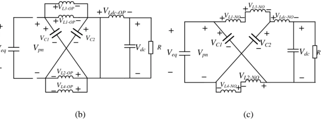
load is supplied by the MR and the Z-source network. The equivalent circuit is shown in Fig.3(c). It can be seen that the energy stored in the capacitors is supplied by matrix rectifier. f L a V b V c V app S apn S f C anp S ann S bpp S bpn S bnp S bnn S cpp S cpn S cnp S cnn S 1
C C2
1 S 1 L 2 L dc L C R (a) R eq V pn V 1 C V 2 C V 1 L V 2 L V Ldc OP V dc V eq V pn V 1 C V 2 C V 1 L V 2 L V Ldc NO V dc V R
(b) (c)
Fig.3. (a) The proposed Z-source matrix rectifier (b) Equivalent circuit of open-circuit zero state (c)
Equivalent circuit ofnon-open-circuit zero state
According to the chosen MR modulation scheme, the average output voltage Veqof
MR can be expressed as follows [26]:
0
3
( ) ( ) ( ) cos
2
dc u a b v a c a a im i
Vim is the amplitude of the input phase voltage and iis input power factor angle. From (4), we know that the output voltage range of the matrix rectifier can be (0 ~ 1.5)Vim. Due to the symmetry of Z-source network, the values of inductances and capacitors are usually chosen to be equal, L1 = L2 =L and C1 = C2 = C. Form the
equivalent circuit, we can obtain the equations for Z-source inductors and capacitors:
1 2
L L L
V V V , VC1VC2 VC (5) As shown in Fig.3 (b), it can be shown that:
L OP C
V V , VLdc OP Vdc (6)
Similarly, we can obtain from Fig.3 (c): L NO eq C
V V V , VLdc NO VC Vdc VL NO (7)
Where Veq is the dc-link voltage, and Vdc is the dc output voltage. VLdc-OP and VLdc-NO
are the filter inductor voltages in the open-circuit zero state and non-open-circuit zero state. Similarly, VL-OP and VL-NOare the Z-source inductor voltages.
The average voltage across the inductor over one switching period should be zero in steady state, therefore from (6) and (7) :
0( C) 1( eq C) 0
T V T V V (8)
Hence, 1
1 0
1 1 2
C
eq
V T D
V T T D
(9)
Similarly, applying volt-second balance to filter inductor Ldc,
0( dc) 1(2 C eq dc) 0
T V T V V V (10)
Where T0 is the interval of the open-circuit zero state, D is the open-circuit duty cycle.
We can obtain the relationship between Vdc and Veq from (10):
1
1 0 dc
eq
V T
Therefore the boost factor Bz can be derived: 1 1 0 1 1 2 dc z eq
V T D
B
V T T D
(12)
From (4) and (12), the output voltage can be expressed by:
3 cos
2
dc im i z
V m V B (13)
Where 0cosi 1and0 m 1. M(M m cosi) is the modulation index with a value
range between 0 and 1. So, the output voltage range of the ZSMR
is(0 0.866) Bz 3Vim. The voltage transfer ratio of ZSMR can be obtained:
3 3 1
2 2 1 2
3
dc
Z z
im
V D
G M B M
D V
(14)
B SL-ZSMR Topology Analysis
In [20], a SL cell is introduced into the Z-source network to enlarge voltage-boost ability. Consequently, the SL-ZSMR is proposed as shown in Fig.4(a). The inductors of the Z-source network are replaced by the SL cell, and the other parts have not been changed. The top SL cell consists of two inductors (L1 and L3) and three additional
diodes(D1, D2 and D3). Similarly, the bottom SL cell consists of L2, L4, D4, D5, D6.
f L app S apn S f C anp S ann S bpp S bpn S bnp S bnn S cpp S cpn S cnp S cnn S 1
C C2
dc L R 1 D 2 D 3 D 1 L 3 L 4
D L2
4
R
Veq
VL1-OP
VL2-OP
VC2
VC1
Vdc
Vpn
VL4-OP
VL3-OP V
Ldc-OP
R
Veq
VL1-NO
VL2-NO
VC2
VC1
Vdc
Vpn
VL3-NO
VL4-NO
VLdc-NO
(b) (c)
Fig. 4. (a)The proposed switched-inductor Z-source matrix rectifier (b) Equivalent circuit of
open-circuit zero state (c) Equivalent circuit of non-open-circuit zero state.
The same states also exist in SL-ZSMR: including the open-circuit zero state and non-open-circuit zero states. If switch S1 is on, the proposed SL-ZSMR operates in an
open-circuit zero state. For the top SL cell, D1 and D2are on, and D3 is off. L1and L3
are charged by C1 in parallel. For the bottom SL cell, D4and D5 are on, and D6 is off. L2 and L4 are charged by C2 in parallel. Its equivalent circuit is shown in Fig.4 (b). It
can be shown that both the top and bottom SL cells perform the same function, absorbing the energy stored in the capacitors. If switch S1 is off, SL-ZSMR operates
in the non-open-circuit zero state. For the top SL cell, D1 and D2are off, and D3is on.
L1 and L3are connected in series. D4 and D5are off, and D6is on in the bottom SL cell.
L2and L4 are connected in series. The equivalent circuit is shown in Fig.4 (c) and the
energy stored in inductances is transferred to the main circuit.
For the convenience of mathematical derivation, the values of inductances and capacitors are usually chosen to be equal. Therefore the Z-source capacitor voltage is:
1 2
C C C
V V V (15)
According to the equivalent circuit in Fig.4 (b), we have
1 3
L OP L OP C
1 3
eq C L NO L NO
V V V V , VLdc NO VC (VL1NO VL3NO)Vdc (17)
Applying the volt-second balance principle to L1, it can be shown that the
corresponding voltage across L1 during non-open-circuit zero state, VL1-NO, can be
expressed by:
1
1
L NO C
D
V V
D
(18)
Applying the volt-second balance principle to L3, we have:
0 C 1( eq C L1 NO) 0
T V T V V V (19)
Hence,
1 2
1 1 3
C C C eq
D
V V V V
D
(20)
Applying the volt-second balance principle to Ldc, the following equations can be
obtained from (16) and (17):
0( dc) 1( C L1 NO L3 NO dc) 0
T V T V V V V (21)
This gives the relationship of Vdc and Veq:
2
1 1 3
dc
eq
V D
V D
(22)
So, BSL, the boost factor of SL-ZSMR, can be expressed as: 2
1 0 1
1 0
( 2 ) 1
2 1 3
SL
T T T D
B
T T D
(23)
Similarly, the voltage transfer ratio of SL-ZSMR can be obtained:
2
3 3 1
2 2 1 3
3
dc
z s SL
im
V D
G M B M
D V
(24)
C. TL-ZSMR Topology Analysis
inductors (L11, L12, L21, L22), four additional diodes (D1, D2, D3 and D4) and two
capacitors (C1 and C2). The combination of L11-L12-D1-D3 performs the function of the
top TL cell and the combination of L21-L22-D2-D4 performs the function of the bottom
TL cell. 1 D 12 L 11 L 3 D 1
N N2
f L app S apn S f C anp S ann S bpp S bpn S bnp S bnn S cpp S cpn S cnp S cnn S 1 C 2 C dc L C R 1 S 22
L L21
2
D N2 N1 4 D a u b u c u (a) VL11-OP Veq VC2 VC1 Vdc
Vpn R
N1 N2
L22 N1 N2 Ldc OP V VL12-OP VL21-OP VL22-OP VL11-NO
Veq Vpn Vdc
Ldc NO V VL12-NO VL21-NO VL22-NO R N1 N2
N1 N2
(b) (c)
Fig.5. (a)The proposed tapped-inductor Z-source matrix rectifier (b) Equivalent circuit of
open-circuit zero state (c) Equivalent circuit of non-open-circuit zero state
If switch S1 is on, then the TL-ZSMR operates in the open-circuit zero state. For the
top TL cell, D1 is on, and D3 is off. L11is charged by C1 in parallel. For the bottom TL
cell, D2is on, and D4 is off. L21 is charged by C2 in parallel. The equivalent circuit is
shown in Fig.5 (b). It can be seen that both the top and bottom TL cells perform the same function to absorb the energy stored in the capacitors. In the non-open-circuit zero state, the S1 is off. For the top cell, D1 is off and D3 are on. L11 and L12 are
connected in series. For the bottom TL cell, D2 is off, and D4 is on. L21 and L22 are
in tapped-inductor cells is transferred to the main circuit. The capacitor C1 is charged
by Veq via the bottom TL cell, hence the capacitor C2 is charged via the top TL cell.
The inductors and capacitors are usually chosen to be equal.
1 2
C C C
V V V (25) For the TL cells, their turn ratios are also set to be the equal, NN2/N1, where N1
is the number of winding L11and L21, and N2 is the number of winding L12 and L22.
With these inductive symbols defined, the expressions relating them can be deduced,
2 2
1
11 21
1 2
2 2
2
12 22
1 2
1
( ) ( )
1
( ) ( )
1 N
L L L L
N N N
N N
L L L L
N N N
(26)
Besides the self-inductances, the mutual inductance LM of the TL cells should also
be considered, since it provides a means for measuring energy coupling efficiency within each TL cell. For an ideal TL cell whose coupling coefficient k is 1, LM can be
simplified to:
11 12 2
(1 )
M
N
L k L L L
N
(27)
As for the TL cells, current flowing through L11 as an example is noted to increase
during open-circuit zero state, and decrease during non-open-circuit zero state. From the equivalent circuit in Fig.5 (b), we can obtain:
11 21
L OP L OP C
V V V , VLdc OP Vdc (28)
According to the equivalent circuit in Fig.5 (c), we have:
11 12
eq C L NO L NO
V V V V ,VLdc NO VC(VL11NOVL12NO)Vdc (29)
Where VL11-OP and VL12-OP are the voltages for tapped-inductor winding L11 and L12 in
open-circuit zero state. Similarly, VL11-NO and VL12-NO are the voltages in
non-open-circuit zero state.
open-circuit zero state:
11
11 1
L S L OP
d
V N
dt
, 12 2 11
L M
L OP
d
V N
dt
(30)
11
L S
is the self magnetic flux produced by iL11-op for linking the coil of L11. In contrast,
11
L M
is the mutual magnetic flux produced by iL11-op for linking the coil of L12. For a
perfectly coupled TL, L11S and L11M are equal, inferring that VL12-OP can be
rewritten as:
11
12 1 11
L S
L OP L OP
d
V NN NV
dt
(31)
Applying the volt-second balance principle to L11, the corresponding voltage across
L11 during non-open-circuit zero state, VL1-NO, can be expressed:
11
1
L NO C
D
V V
D
(32)
Applying the volt-second balance principle to L12, we have
0 L12 OP 1 L12 NO 0
T V TV (33)
Hence,
12
1
L NO C
ND
V V
D
(34)
From (28)to (34), we have:
1 1 2
C eq
D
V V
D DN
(35)
From (28) ,(29)and (35), we have:
0( dc) 1( C L11 NO L12 NO dc) 0
T V T V V V V (36)
So,
(1 )(1 ) 1 2
dc
eq
V D DN
V D DN
(37)
0 0
0 0
(1 / )(1 ( / ) ) (1 )(1 )
1 2( / ) ( / ) 1 2
TL
T T T T N D DN
B
T T T T N D DN
(38)
Similarly, the voltage transfer ratio of TL-ZSMR can be obtained
3 3 (1 )(1 )
2 2 1 2
3
dc
z T TL
im
V D DN
G M B M
D DN V
(39)
IV. FEATURES COMPARISON
A. Feature Comparisons Of Proposed Rectifiers
The boost factors B versus D for the ZMSR, SL-ZSMR and TL-ZSMR with various turn ratios are shown in Fig.6 (a). When N=0,
1-1- 2 D B
D
, the secondary winding of
tapped inductor is omitted, and the TL-ZSMR becomes a ZSMR. When N =1,
2
1 1 3
D B
D
, the boost factor is equal to that of SL-ZSMR. It can be seen that the
voltage-boost capability of the proposed TL network at a specified D value improves as N increases. The voltage stress for switching device is different under different voltage-boost levels. Fig.6(b) shows the voltage stress comparison of switching device S1 for the ZMSR, SL-ZSMR and TL-ZSMR. As shown in Fig.6(b), for the
same output voltage gain, the proposed TL-ZSMR has a lower voltage stress compared ZSMR and SL-ZSMR as N increases.
(c)
Fig.6. (a)Boost ability of proposed ZMSR,SL-ZSMR and TL-ZSMR with various turn ratios of N
(b)Switching device S1 voltage stress of proposed ZMSR,SL-ZSMR and TL-ZSMR with various
turn ratios of N (c) Voltage conversion ratios versus modulation index of proposed ZMSR,
SL-ZSMR and TL-ZSMR with various turn ratios of N.
Fig.6(c) shows the voltage conversion ratios versus modulation indices of the proposed three rectifiers. The proposed three rectifiers can all provide higher voltage boost inversion by using the same modulation index. For the same output voltage gain, the proposed TL-ZSMR uses a higher modulation index todecrease the total harmonic distortion value and improve the rectifier output quality. Table I compares the corresponding governing equations of the proposed ZSMR, SL-ZSMR and TL-ZSMR. From Table I, it can be seen that the TL-ZSMR has the higher voltage stresses of diodes and capacitors due to its stronger voltage-boost ability in the same D.
TABLE I
Stress comparison to three topologies
ZSMR SLZSMR TLZSMR(N=2)
/
Vc Veq 1
1 2 D
D
1 1 3
D D
1 1 4
D D
/
Vdc Veq 1
1 2 D
D
2
1 1 3
D D
2
1 2
1 4
D D
D
Diode stress 0 1 3 D D
(D1)
1 1 3
D D
(D3)
2 1 4
D D
(D1)
2(1 )
1 4 D D
(D3)
3 Vdc G
Vim
3 1
2 1 2
D M
D
2
3 1
2 1 3
D M
D
2
3 1 2
2 1 4
D D
M
D
B. Differences Among Proposed Rectifiers And Converters Published In Other References
The converters [4-7] are the traditional ac-ac matrix converters without the Z-source network and the voltage-boost function. The converters [11, 12] are the voltage-boost ac-ac Z-source matrix converters but without the ac-dc rectifier function. The converters [15-18], different from ac-ac Z-source matrix converters [11, 12], can realize the ac-dc rectifier function but a buck Z-source matrix rectifier. The differences among proposed rectifiers and the converter [15] by “keping you” are analyzed as follows.
Firstly, the topology differences among proposed rectifiers and converter [15] are shown in Table II. From Table II, it can be seen that the component counts of proposed rectifiers are different from those of the converter [15]. As shown in Fig.7(a), the converter [15] includes three switches (X1, X2 and S1) and a battery. The three switch count and the switch position are different from those of proposed rectifiers and proposed rectifiers do not include the battery, which are the topology differences among proposed ZSMR and the converter [15]. From Fig.4 and Fig.5, it can be seen that the proposed SL-ZSMR and TL-ZSMR exist the larger topology differences compared with the converter [15].
need different operation principles. The proposed ZSMR, SL-ZSMR and TL-ZSMR introduce the additional open-circuit zero state where the switch S1 is turned on and
all the switching devices to realize the voltage-boost ac-dc function. The auxiliary switch S1 ensures the energy to flow from the capacitors (C1 and C2) to the inductors
(L1 and L2) and provides the conduction path for the capacitor C and inductor Ldc. The
equivalent circuits of proposed ZSMR, SL-ZSMR and TL-ZSMR are shown in Fig.3, Fig.4 and Fig.5.
Differently, the auxiliary switch X1 and the diode D of the rectifier in [15] mainly block the energy flow and the current of three-phase ac sources to the battery. Fig.7(b) shows the equivalent configuration of the converter [15] in ac-dc rectification mode. In this mode, the switch X1 and S1 are in the OFF-state; X2 and X3 are closed. As shown in Fig.7(b), the Z-source network of the converter in [15] under ac-dc rectification mode serves as the filter at the dc side. The converter in [15] without the voltage-boost process is a ac-dc buck rectifier, which is essential difference from proposed rectifiers.
L1 C1
R L2 C2
S1 app S apn S anp S ann S bpp S bpn S bnp S bnn S cpp S cpn S cnp S cnn S La,b,c Ca,b,c Three-phase AC source /load X3 X1 X2 Vdc,g Vdc,s L1 C1 L2 C2 Vdc,g La,b,c Ca,b,c a V b V c V app S apn S anp S ann S bpp S bpn S bnp S bnn S cpp S cpn S cnp S cnn S R
(a) (b)
Fig.7. (a) The general topology structure in [15] and (b) Equivalent structure of the converter in
[15] when it is in the ac-dc rectification mode.
The topology differences among proposed rectifiers and rectifiers [15]
Topology ZSMR SL-ZSMR TL-ZSMR rectifier in [15]
Numbers of switches 13 13 13 17
Numbers of diodes 0 6 4 1
Numbers of inductors 6 8 6 5
Numbers of capacitors 6 6 6 5
V. SIMULATION VERIFICATION
To verify the theoretical analysis for the proposed ZSMR, SL-ZSMR and TL-ZSMR, simulations are set up for the topologies shown in Fig.3(a), Fig.4(a) and Fig.5(a). The balanced three-phase input voltage for these three simulations is 20V/50Hz, and the load per phase is 10Ω. For the ZSMR L1=L2=2mH and
C1=C2=470uF; for the SL-ZSMR L1=L2=L3=L4=1mH and C1=C2=470uF; and for the
TL-ZSMR L11=L21=0.22mH, L12=L22=0.88mH and C1=C2=470uF. In the simulations,
all the components are assumed to be ideal.
The simulation results are shown in Fig.8, Fig.9 and Fig.10 for the ZSMR, SLZSMR and TLZSMR respectively for the condition when M=0.8 and D=0.1. It can be seen from Fig.8 that the capacitor voltage VC and output voltage Vdc are 26.5V
which is closed to the theoretical value 27V calculated from (9) and (13). Then, from (12) and (14), we get the voltage transfer ratio G=0.779 and the boost factor B=1.125. Fig.8 also shows the enlarged waveform of Z-source inductor current IL1. It can be
seen from the Fig.8 that the inductor charges or discharges when S1 is turned on or
0.02 0.025 0.03 0.035 0.04 20 30 40 50 60 (V )
70input voltage of Z-source
Time(s) 10
0.02 0.03 0.04
(V
)
capacitor voltages Vc
10 20 30 40
0
Time(s) 0.05 0.06
(a) (b)
0.02 0.03 0.04 0.05 0.06 Time(s) (V ) 10 20 30 40 0
output voltages Vdc
0.1008 0.1012 0.1016
current of IL1
(A ) 0.5 1.0 1.5 2.0 Time(s) 0.1004
(b) (d) Fig.8. Simulation results of ZSMR
As shown in Fig.9, it can be seen that the capacitor voltage VC is 30.2V close to
the theoretical value of 30.86V, and the output voltage Vdc is 33.5V which is close to
the theoretical value of 33.94V. It is obvious that the input voltage of Z-source network, the capacitor voltage and the output voltage for SL-ZSMR are much higher than those of the ZSMR for the same D and M. So, the corresponding voltage transfer ratio, 0.975 from (24), is greater than ZSMR, verifying that the voltage-boost ability of the circuit is significantly higher.
0.02 0.025 0.03 0.035 0.04
input voltage of Z-source
10 20 30 40 50 60 70 Time(s)
0.02 0.03 0.04 0.05
capacitor voltages Vc
Time(s) (V ) 10 20 30 40 0 0.06
(a) (b)
output voltages Vdc
0.02 0.03 0.04 0.05 Time(s) (V ) 10 20 30 40 0 0.06
current of IL1
Time(s)
0.1004 0.1008 0.1012 0.1016
(b) (d)
Fig.9. Simulation results of SL-ZSMR
The voltage transfer ratio can be realized optimally by the proposed TL-ZSMR, as shown in Fig.10. From Fig.10, it can be seen that the capacitor voltage VC and output
voltage Vdc are consistent with the theoretical values, and the input voltage of
Z-source network is the highest of the three topologies. The corresponding voltage transfer ratio is 1.24 calculated by equation (39). Obviously, when D and M are the same, the voltage transfer ratio of the TL-ZSMR is the highest. Fig.10 also shows the enlarged waveforms of the current of tapped-inductor LL11 and LL12, and it can be seen
that the waveforms of IL11 and IL12 are complementary, which is consistent with the
theoretical analysis. So, by the simulations, we have verified the availability of the proposed rectifiers.
0.02 0.025 0.03 0.035 0.04
input voltage of Z-source
Time(s)
(V
)
10 20 30 40 50 60 70 80
capacitor voltages Vc
0.02 0.03 0.04 0.05
Time(s)
(V
)
10 20 30 40
0
0.06
(a) (b)
output voltages Vdc
0.02 0.03 0.04 0.05 Time(s)
(V
)
10 20 30 40
0
0.06 50
Time(s)
current of IL11
2.0 4.0 8.0 10.0 12.0
6.0
(A
)
0.1006 0.1008 0.1010 0.1012 0.1014 0.1016
(b) (d)
1.0 2.0 3.0 4.0 5.0 6.0
0.1006
Time(s)
0.1008 0.1010 0.1012 0.1014 0.1016
(A
)
Fig.10. Simulation results of TL-ZSMR
VI. EXPERIMENTAL RESULTS
The same parameters are chosen to construct a testing hardware circuit according to the simulations. The switching frequency is 5 kHz. The switch devices are 1MBH60D-100 and the drive circuit, DA962D6, can independently drive six IGBTs at the same time. The switch turn-on time is about 0.3us, and the turn-off time is about 0.85us. The commutation delays are less than or equal to 1.15us, the addition both turn-off time and turn-on time. The core material of ZSMR utilizes H5C2 and the number of turns is 21. The core material of SL-ZSMR also utilizes H5C2 and the number of turns is 14. The core material of TL-ZSMR is PC40. The primary turn number is 18 and the secondary turn number is 36. The average dc accuracy of the oscilloscope is about +/-3%. The modulation scheme and control strategy are implemented in a high-performance DSP (TMSF320F2812). Fig.11, Fig.12 and Fig.13 correspond to the experiment results for the ZSMR, SL-ZSMR and TL-ZSMR, respectively. From Fig.11, Fig.12 and Fig.13, it can be seen that the experimental results are consistent with the simulation results. The capacitor voltage values and the output voltage values for the ZSMR, SLZSMR and TLZSMR are listed in Table III. The capacitor voltage value for ZSMR is about 25.9V close to the theoretical value
1 0.9
24 27
1 2 0.8
C eq
D
V V V
D
, and theoutput voltage value is about 25.3V. So, the
corresponding voltage transfer ratio is 0.730 3
dc z
im
V G
V
, which is 0.049 less than
Input voltage of Z-source network Vpn (20V/div)
Time divison: 2ms
Output dc voltage Vdc (20V/div)
Z-source capacitor voltage Vc (20V/div)
Time divison: 10ms
(a) (b)
Z-source inductor current IL1(2A/div)
Time divison: 100us
(c)
Fig.11. Experiment results of ZSMR
TABLE III
ZSMR SLZSMR TLZSMR(N=2) VC 25.8V 28.9V 34.8V
Vdc 25.8V 31.9V 42.1V
Fig.12 shows the Z-source input voltage for SL-ZSMR, whose magnitude is higher than the ZSMR. From the Table III, it can be seen the capacitor voltage for the SL-ZSMR is about 28.9V close to the theoretical value 1 1 0.1 24 30.85
1 3 1 3 0.1
C eq
D
V V V
D
. The output voltage is about 31.9V close to
the theoretical value
2 2
1 1 0.1
24 33.94
1 3 1 3 0.1
dc eq
D
V V V
D
, which is higher 6.6V than
Input voltage of SL-Z-source network Vpn (20V/div)
Time divison: 2ms
Output dc voltage Vdc (20V/div)
SL-Z-source capacitor voltage Vc (20V/div)
Time divison: 10ms
(a) (b)
SL-Z-source inductor current IL1(2A/div)
Time divison: 100us
(c)
Fig.12. Experiment results of SL-ZSMR
The experiment results for the TL-ZSMR are shown in Fig.13, which includes the Z-source input voltage, output voltage, capacitor voltage and the tapped-inductor current. It can be seen that the capacitor voltage is about 34.8V close to the theoretical
value 1 1 0.1 24 36
1 4 1 4 0.1
C eq
D
V V V
D
. The output voltage is about 42.1V close to
the theoretical value (1 2 )(1 ) (1 2 0.1)(1 0.1) 24 43.2
1 4 1 4 0.1
dc eq
D D
V V V
D
, which is
Input voltage of TL-Z-source network Vpn (20V/div)
Time divison: 2ms
Output dc voltage Vdc (20V/div)
TL-Z-source capacitor voltage Vc (20V/div)
Time divison: 10ms
(a) (b)
Time divison: 100us TL-Z-source inductor current
IL11(5A/div)
IL12(2A/div)
(c)
Fig.13. Experiment results of TL-ZSMR
VII CONCLUSION
This paper has presented a novel Z-source matrix rectifier by combining a matrix rectifier and three Z-source networks. The proposed rectifiers introduce a modified modulation strategy by taking an open-circuit zero state into the traditional zero states to overcome a voltage-boost drawback in traditional matrix rectifier. And the new increased Z-source network also serves as energy storage and guarantees double filtration grade at the output of the rectifier. Finally, the validity of the three topologies considered and the modified modulation strategies for the proposed ZSMR, SL-ZSMR and TL-ZSMR circuits is verified using both the simulation and experiment results.
[1] Lozano-Garcia, J. M., Ramirez, J. M.: ‘Voltage compensator based on a direct matrix converter without energy storage’, IET Power Electron., 2015, 8, (3), pp.
321-332.
[2] Huber L, Borojevic D. Space vector modulated three-phase to three-phase matrix converter with input power factor correction[J]. Industry Applications, IEEE Transactions on, 1995, 31(6): 1234-1246.
[3] Ortega, M., Jurado, F., Carpio, J.: ‘Control of indirect matrix converter with bidirectional output stage for micro-turbine’, IET Power Electron., 2012, 5, (6), pp. 659-668
[4] R. Cárdenas, R. Peña, R. Peña, and J. Clare, “Experimental validation of a space
vector modulation algorithm for four-leg matrix converters,” IEEE Trans. Ind. Electron., vol. 58, no. 4, pp. 1282-1293, Apr. 2011.
[5] Jahan, H. K., Banaei, M. R.: ‘Implementation of a stepped down frequency eight switches matrix converter suitable for microturbine generation’, IET Power Electron., 2014, 7, (5), pp. 1092-1098
[6] M. Hamouda, H. F. Blanchette, K. Al-Haddad, and F. Fnaiech, “An efficient DSP-FPGA-based real-time implementation method of SVM algorithms for an indirect matrix converter,” IEEE Trans. Ind. Electron., vol. 58, no. 11, pp. 5024–5031,
Nov. 2011.
[7] Shi, T., Huang, Q., Yan, Y., Xia, C.: ‘Suppression of common mode voltage for matrix converter based on improved double line voltage synthesis strategy’, IET Power Electron., 2014, 7, (6), pp. 1384-1395
reference generation for predictive control in a direct matrix converter’, IET Power Electron., 2013, 6, (5), pp. 894-901
[9] Rajendran, S., Govindarajan, U., Parvathi Sankar, D.S.: ‘Active and reactive power regulation in grid connected wind energy systems with permanent magnet synchronous generator and matrix converter’, IET Power Electron., 2013, 7, (3), pp.
591-603
[10] S. Khwan-on, L. De Lillo, L. Empringham, P. Wheeler, and C. Gerada, “Fault-tolerant, matrix converter, permanent magnet synchronous motor drive for
open-circuit failures,” IET Electric Power Appl., vol. 5, no. 8, pp. 654-667, 2011. [11] X. Liu, P. C. Loh, P. Wang, and X. Han, “Improved modulation schemes for indirect Z-source matrix converter with sinusoidal input and output waveforms,” IEEE Trans. Power Electron., vol. 27, no. 9, pp. 4039–4050,Sep. 2012.
[12] S. Khwan-on, L. De Lillo, L. Empringham, P. Wheeler, and C. Gerada, “ A Quasi-Z-Source Direct Matrix Converter Feeding a Vector Controlled Induction Motor Drive,” IEEE Journal of Emerging and Selected Topics in Power Electronics, vol. 3, no. 2, pp. 339-348, 2015.
[13] E. Karaman, M. Farasat, and A. M. Trzynadlowski, “Permanent-magnet synchronous-generator wind-energy systems with boost matrix converters,” in Proc. Energy Convers. Congr. Exposit. (ECCE), 2013, pp. 2977-2981.
[14] S. Lei, X. Haiping, L. Dongxu, Y. Zengquan, “A novel high power factor PWM rectifier inverter for electric vehicle charging station,” in Proc. IEEE Int. Conf. Elect.
Machines and Systems, Beijing, China, pp. 1-6, Aug. 2011.
bidirectional power flow for an integrated starter alternator system,” IEEETrans. Ind.
Appl., vol. 45, no. 1, pp. 239-248, Jan./Feb. 2009.
[16] Keping You, M. F. Rahman; " Analytical Comparison of Conduction and
Switching Losses of A Novel Matrix-Z-Source Converter and A Conventional VSI Converter for Automotive ISA 42 V System ",PESC2006, the 37th IEEE Powver Electronics Specialists Conference, June 18 to 22, 2006, Jeju, Korea.
[17] You Keping and Rahman M.F., “Analysis of conduction and switching losses of a matrix-Z-source converter,” the 7th International Conference on Power Electronics, pp.1071-1076, 2007.
[18] You Keping and Rahman M.F., “A matrix-Z-source converter for automotive integrated starter alternator system,” Proc. IEEE Applied Power Electronics
Conference and Exposition, pp. 273-279, 2008.
[19] F.Z. Peng, “Z-source inverter,” in Proc. IEEE-IAS Annu. Meeting, 2002, pp. 775-781. March/April 2003.
[20] M. Zhu, K. Yu, and F. L. Luo, “Switched inductor Z-source inverter,” IEEE Trans. Power Electron., vol. 25, no. 8, pp. 2150–2158, Aug. 2010.
[21] Soon, J. J., Low, K. S.: ‘Sigma-Z-source inverters’, IET Power Electron., 2015, 8, (5), pp. 715-723
[22] Ahmed, T., Mekhilef, S.: ‘Semi-Z-source inverter topology for grid-connected photovoltaic system’, IET Power Electron., 2015, 8, (1), pp. 63-75.
[24] Nguyen, M. K., Lim, Y. C., Park, S. J., Shin, D. S.: ‘Family of high-boost Z-source inverters with combined switched-inductor and transformer cells’, IET Power Electron., 2013, 6, (6), pp. 1175-1187
[25] M. Zhu, D. Li, P. C. Loh, and F. Blaabjerg, “Tapped-inductor Z-source inverters with enhanced voltage boost inversion abilities,” in Proc. IEEEICSET, Dec. 2010, pp.
1-6.