On the modified active region design of interband cascade lasers
M. Motyka, K. Ryczko, M. Dyksik, G. Sęk, J. Misiewicz, R. Weih, M. Dallner, S. Höfling, and M. Kamp
Citation: Journal of Applied Physics 117, 084312 (2015); doi: 10.1063/1.4913391 View online: http://dx.doi.org/10.1063/1.4913391
View Table of Contents: http://scitation.aip.org/content/aip/journal/jap/117/8?ver=pdfcov Published by the AIP Publishing
Articles you may be interested in
Eight-band k·p modeling of InAs/InGaAsSb type-II W-design quantum well structures for interband cascade lasers emitting in a broad range of mid infrared
J. Appl. Phys. 114, 223519 (2013); 10.1063/1.4843076
onHigh-peak-power strain-compensated GaInAs/AlInAs quantum cascade lasers ( λ ∼ 4.6 μ m ) based on a slightly diagonal active region design
Appl. Phys. Lett. 93, 251110 (2008); 10.1063/1.3054165
Mid-infrared In As ∕ Al Ga Sb superlattice quantum-cascade lasers Appl. Phys. Lett. 87, 211113 (2005); 10.1063/1.2136428
Effects of anisotropic k · p interactions on energy bands and optical properties of type-II interband cascade lasers J. Appl. Phys. 96, 1866 (2004); 10.1063/1.1763243
On the modified active region design of interband cascade lasers
M. Motyka,1K. Ryczko,1M. Dyksik,1G. SeRk,1J. Misiewicz,1R. Weih,2M. Dallner,2
S. Hofling,€ 2,3and M. Kamp2 1
Laboratory for Optical Spectroscopy of Nanostructures, Department of Experimental Physics, Wrocław University of Technology, Wybrzeze Wyspia_ nskiego 27, Wrocław, Poland
2
Technische Physik, University of Wurzburg & Wilhelm-Conrad-R€ ontgen-Research Center€
for Complex Material Systems, Am Hubland, D-97074 Wurzburg, Germany€
3
SUPA, School of Physics and Astronomy, University of St. Andrews, North Haugh, KY16 9SS, St. Andrews, United Kingdom
(Received 16 November 2014; accepted 11 February 2015; published online 25 February 2015)
Type II InAs/GaInSb quantum wells (QWs) grown on GaSb or InAs substrates and designed to be integrated in the active region of interband cascade lasers (ICLs) emitting in the mid infrared have been investigated. Optical spectroscopy, combined with band structure calculations, has been used to probe their electronic properties. A design with multiple InAs QWs has been compared with the more common double W-shaped QW and it has been demonstrated that it allows red shifting the emission wavelength and enhancing the transition oscillator strength. This can be beneficial for the improvements of the ICLs performances, especially when considering their long-wavelength operation.VC 2015 AIP Publishing LLC. [http://dx.doi.org/10.1063/1.4913391]
I. INTRODUCTION
Interband Cascade Lasers (ICLs) based on type II InAs/ GaInSb quantum wells (QWs)1–3 have been successfully used for optical detection of many gases related to environ-mental protection, medical diagnostics, safety and security, in such applications as for instance human breath analysis4 or detection of harmful or toxic gases, e.g., formaldehyde5or nitric oxide.6It has been made possible due to the high sensi-tivity of such laser-based sensors, originating mostly from unique operational characteristics of ICLs, such as, among others: (i) single mode, continuous wave (cw) and high power operation at room or even elevated temperatures,7,8 (ii) broad spectral tunability,9(iii) and low threshold currents and small electrical power consumption10when compared to the main competitor, which are quantum cascade lasers (QCLs). However, the best ICLs’ performances, when regarding the cw mono mode lasing at room temperature, have mostly been obtained for the emission range of about 3–5.5lm. There have also been reported some attempts at longer wavelengths, but these are limited to multimode pulsed lasers at above 6lm (Refs.11and12) or low temper-ature pulsed operation at 7.5 and 10.4lm,13,14 which are usually insufficient for most of the gas detection schemes. Therefore, there is still a strong demand on improvements in the design and performances of the ICLs to extend the spec-tral range in which they become suitable for gas sensing applications and could compete with the QCLs.
There already exist reports on new concepts to expand the possible ICL emission range, e.g., by replacing the ter-nary GaInSb valence band well with a quaterter-nary GaInAsSb layer.15–17 This approach offers simultaneous reduction of the strain and a shift of the optical transition to longer wave-lengths, while preserving a good electron-hole wave func-tions overlap. However, this prospective solution has been found out to have some technological limitations related to
interface quality and nonradiative centers16and lasers of that kind have not been demonstrated yet.
In this work, we explore another optimization concept which is based on the use of additional layers in the QW struc-ture in comparison to the standard “W-shape” design. We con-sider a system of triple InAs layers and double GaInSb layers—see Fig.1, which has already been recognized as very useful from the point of view of wider tunability of the ICLs.9 Hereby, we pay attention to the enhancement of the oscillator strength (OS), potentially beneficial for improvements in the performances of the existing devices or for the extension of the emission wavelength. Shifting the emission into longer wave-lengths denotes naturally a decrease in the OS, if keeping the common design and materials. In order to investigate this issue, two pairs of double and triple QWs have been grown on both GaSb and InAs substrates. Their electronic structure has been calculated within the multiband kp model and optical spectroscopy in the form of modulated reflectivity has been utilized to probe the optical transition energies and intensities experimentally, and thus to verify the theoretical predictions.
II. EXPERIMENTAL
The investigated structures have been grown on (100) oriented InAs (samples A, B) and GaSb (samples C, D) sub-strates, in a solid source molecular beam epitaxy system equipped with valved cracker cells for both antimony and ar-senic. Two of the type II samples have been designed in the “W-like” shape, consisting of two InAs layers and one GaInSb layer (standard double QW design), and two in the form of a triple QW, i.e., three InAs layers and two GaInSb layers—see Fig.1. All the QW details are listed in TableI.
The core part of all the QWs, as indicated in TableI, is always surrounded by 2 nm thick AlSb barriers. In order to enhance the overall optical response, the wells have been repeated five times in all the samples. For the A and B
structures on InAs, the QW part is preceded by 200 nm InAs buffer. The wells are separated by 25 nm thick GaAs0.08Sb0.92
layers lattice matched to InAs, and the entire structure is termi-nated with the same GaAs0.08Sb0.92 layer. For the samples C
and D on GaSb substrate, the active part is similarly con-structed, with a difference in the buffer layer being GaSb in this case, and the separating barriers and the cap layer, which are also made of GaSb.
In order to measure photoreflectance (PR) in a wide spectral range, i.e., optical spectra which are sensitive to the transition oscillator strength,15 we used a setup based on a Fourier-transformed (FT) and vacuumed Bruker Vertex 80v spectrometer operated in a step- or rapid-scan (for fast differ-ential reflectivity measurements18) mode. This is addition-ally equipped with a reflectance/transmittance unit providing 12angle for incident probing light, for experiments employ-ing an additional modulated laser beam. Similar FT-based approaches have been demonstrated as very efficient for probing QW transitions in the mid infrared range by several groups.19–22 In our case, a liquid-nitrogen cooled MCT (mercury cadmium telluride) photodiode was used as a de-tector. In this measurement configuration, the pump beam was provided by the 660 nm line of a semiconductor laser diode, which was mechanically chopped at a frequency of 275 Hz. Phase sensitive detection of the optical response was performed using a lock-in amplifier. Further experimental details can be found elsewhere.21
III. RESULTS AND DISCUSSION
Figure 1 shows the band diagrams for sample A (left panel) and sample B (right panel), together with the probability
densities of the first confined electron state (black curve) and the first confined heavy hole state (red curve). It visualizes the expected increase in the overlap between the electron and hole wave functions when increasing the number of potential wells. The situation looks qualitatively very similar for samples C and D. The overlap integral change translates directly into the change of the optical transition oscillator strength defined as
f P
2
if
EfEijhFfð Þjz Fið Þijz
2
; (1)
wherePifis the bulk momentum matrix element defined
ba-sically by the Kane energy, whereas jhFfðzÞjFiðzÞijis the so
called envelope wave function overlap integral.
Figure2shows photoreflectance spectra obtained for all the four investigated samples. The red solid line curves rep-resent the result of the fitting procedure assuming the PR line-shape according to the commonly used formula15,23,24
DR
R ð Þ ¼E Re Xn
j¼1
Cjei#jðEEjþiCjÞmj
" #
; (2)
wherenis the number of optical transitions and independent spectral functions used in the fit,Cjand#jare the amplitude
and phase parameters, Ej and Cj are the energy and the
broadening parameter of the transitions, respectively. The fit-ting curves are shown as solid red lines together with the moduli of the individual resonances (dashed lines) obtained according to Eq.(3)
Dqð Þ ¼E jCj
EE0
ð Þ2þC2
h im
2
: (3)
[image:3.612.83.267.63.221.2]First of all, it is visible that the introduction of the additional layers in the QW structure, i.e., expansion into the triple QW
TABLE I. The layer structure of the investigated QWs.
Sample:
InAs (width, layer numbers)
GaInSb (width, content, layer numbers)
Sample A 2.9 nm, 2 layers 3 nm, Ga0.76In0.24Sb layer, 1 layer
Sample B 2.9 nm, 3 layers 3 nm, Ga0.76In0.24Sb layer, 2 layers
Sample C 1.4 nm, 2 layers 3.5 nm, Ga0.665In0.335Sb layer, 1 layer
[image:3.612.317.561.506.720.2]Sample D 1.4 nm, 3 layers 3.5 nm, Ga0.665In0.335Sb layer, 2 layers
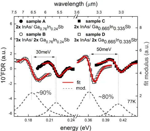
FIG. 2. Low temperature (77 K) photoreflectance spectra for the investigated samples: A—full circles, B—open circles, C—full squares, and D—open squares. The red solid lines represent the line shape fits, whereas the dashed peaks correspond to the moduli of the respective PR features.
FIG. 1. Band structure diagram of the investigated W-shape double QW (a), and the modified triple QW design (b), together with calculated probability densities of the confined electron and heavy holes states (example for sam-ples A and B).
[image:3.612.50.297.683.764.2]system, shifts the fundamental transition energy to the red. Such a behavior is expected when taking into account the effectively wider confinement potential for the carriers. When comparing the spectra of samples A and B, and then samples C and D, energy shifts of 30 meV and 50 meV are obtained, respectively. These translate into wavelength shifts of1000 nm and400 nm, respectively. This indicates that such an active region modification can indeed lead to a broader tunability, as already suggested in the recent report,9 but mainly it shows that such a change makes the tuning of the emission into the longer wavelengths easier, which can be one of the advantages of this kind of modified triple-QW-based active region design.
Further, we have used the property of the modulated reflectivity spectra, i.e., probing the intensity of the optical transitions,25–27 where the integrated spectral feature inten-sity corresponds to the transition oscillator strength. The for-mer can directly be obtained as an area under the moduli of the particular spectral lines, i.e., under the dashed curves in Fig.2. It should be mentioned here that transition intensities determined in such a way can be compared between the spectra of different samples only if one can assume that the modulation efficiency is approximately the same. This is the case for the samples investigated here: they have similar layer structure and the experimental conditions have been preserved.
For the two pairs of the samples, we have obtained an increase in the PR intensity by about 90% and 80% when changing from the double to the triple QW design (compar-ing sample A with B and then sample C with D). For further analysis, we assume that the value ofP2
if=ðEf EiÞ(in Eq. (1)) does not change significantly between various QW sam-ples investigated here. We can also replace the initial and final states with the holehand electronestates, respectively, and the oscillator strength can be rewritten in the following form:
f jhFeðzÞjFhðzÞij2¼ ð 1
1
FeðzÞ FhðzÞdz
2
; (4)
i.e., considered as proportional to the squared wave func-tions overlap. Hence, this squared overlap will further be treated as an approximate figure of merit of the transition intensity and will serve as a quantity to be confronted with the experiment.
Figure 3 presents the calculated transition energies (panel (a)) and the calculated squared overlap integral of the electron and hole wave functions (panel (b)) as a func-tion of the InAs layer width of the QWs. The calculafunc-tions have been performed within the eight-bandkpformalism28 including the strain effect, with all the methodology similar to that described in one of our previous works.17 All the material parameters have been taken from Ref.29and have been interpolated linearly for the corresponding ternary compounds, except for the band gap. In the case of the band gap determination as a function of alloy composition, we included the respective bowing parameters.29 Any addi-tional structural effects occurring for heterostructures of
this material combination, as e.g., disturbance of the con-finement potential due to the existence of a GaAs-like or InSb-like interfaces30,31nor interface intermixing have not been included in the calculations.
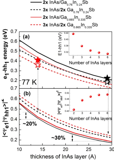
Solid lines in Fig.3represent the results of calculations for the samples with the standard "W" shape double QW profile, like sample A (black solid curves) and sample C (red solid curves), whereas the dashed lines correspond to the cal-culations performed for the modified design structures with three InAs layers: sample B—black dashed lines, and sample D—red dashed lines. Star symbols correspond to the ener-gies of the fundamental transitions obtained from the PR measurements (from spectra shown in Fig. 2) for all the investigated samples. It is seen that the symbols match the calculated dependencies very well. These results show both theoretically and experimentally that the QW multiplication in such a type II system offers the intrinsic property of shift-ing the optical transitions to the red, with respect to common W-design QWs. Therefore, this can be a useful solution for longer wavelength emission, as long as the transition oscilla-tor strength can be kept sufficiently large.
When considering the overlap integrals, we can compare the solid curves with the dashed ones to observe the QW design modification. In the entire range of the InAs layer widths, we can see an increase in the squared overlap inte-gral of about 30% and 20% for sample B (comparing to sam-ple A) and samsam-ple D (comparing to samsam-ple C), respectively. The calculated enhancement of the squared wave functions overlap integral after introducing additional layers in the
[image:4.612.339.534.63.340.2]QW structure (with respect to the standard “W-shaped” QWs) agrees qualitatively with the experimental data reflect-ing the transition intensities. In spite of the clear and con-firmed tendencies observed both in the calculation and in the experiment, the relative numbers concerning the intensities do not agree very exactly. This is however related to some limitations on both the experimental and the theoretical side. In the modulated reflectivity measurements, there always remains a certain inaccuracy related to the proper alignment of the probe and pump beam spots on the surface of the sam-ple, and hence keeping exactly the same photo-modulation efficiency for each sample is difficult. On the other hand, when regarding the calculations, the QW layout is assumed the simplest possible and such issues as the band bending at the interfaces, the interface intermixing nor the existence of any intermediate interfacial layers have not been taken into account.
The insets in Fig.3show how both the transition energy and its intensity would change with further increase in the number of wells (layers) in this kind of QW system for the case corresponding to the previously discussed samples C and D. As expected, the dependencies start saturating and although the possible use of a fourfold repetition of the InAs QW can give an improvement in the oscillator strength by several percent, so it is still perhaps worth consideration in the practical realization, further switching into five wells enhances the transition intensity rather negligibly. The de-pendence on the number of wells in the system looks qualita-tively very similar also for samples A and B; therefore, it is not shown in Fig.3for clarity.
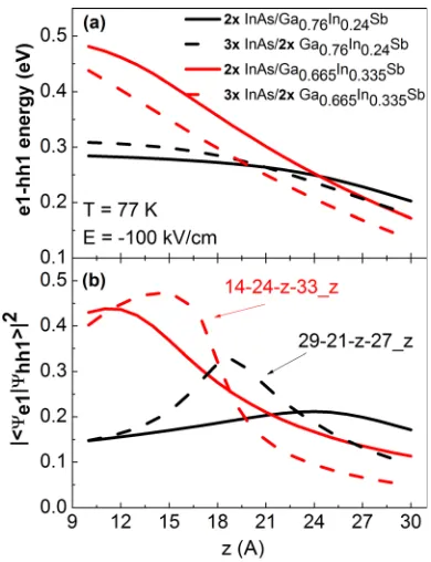
In order to predict the usefulness of the discussed approach and the OS enhancement on the full laser structure, in which the active region is in an external electric field, sim-ulations taking that effect into account have also been per-formed. Figure 4 shows the calculated fundamental transition energy (top panel) and the squared wave functions overlap (bottom panel) for the typical “W” QW (solid lines) and the triple design QW (dashed lines) under the external electric field equal to 100 kV/cm (a value characteristic for the ICL devices). The results are plotted as a function of pa-rameter “d,” which is the thickness of the one (or two) InAs layers in the case of the double (triple) QW designs. The entire layer structure must be modified accordingly in the electric field in order to compensate its influence, mainly on the oscillator strength. As the electric field bends the struc-ture, the electron and hole probability densities are shifted in the opposite directions, which leads to the overlap reduction (and simultaneous shift of the transition energy). This can be balanced if the structure is made asymmetric. For the com-mon W-shape double QW design, it is sufficient to just change the thickness of one of the InAs layers (the tuned layer thickness is named “d” in Fig. 4). The situation is much more complex in the case of the triple QW design. First of all, there need to be modified at least two of the three InAs wells to effectively push back the electron probability density and compensate the electric field influence. Second, as the holes are confined in two GaInSb layers now, this must be corrected by changing the thickness of one of these layers as well. Exemplary results of such modifications are
shown in Fig. 4 with the dashed lines. The widths of the layers in the triple QW structure are given in the figure. Of course, one could propose other design corrections, but disre-garding the details the main conclusion is that it is always possible to maximize the oscillator strength of the transitions in such a multiple type II QW system in the electric field, and that the structure with triple InAs QWs always offers larger values of the OS. Therefore, this also further proves the usefulness of this multiplied QW approach.
It is also worth mentioning that in order to verify pre-liminarily the effect of the increased number of wells in the active region such a modification has been included in the simulations of the optical field distribution within the wave-guide and the resulting confinement factor. The obtained modal overlap with the active region has appeared to be higher for the triple QW design in spite of the slightly wider active region. This is related to the larger refractive index of GaInSb layers, which tends to “concentrate” the optical mode at the core of the structure. Thus, the thicker active region has in fact a positive effect on the confinement of the mode, and therefore, when combined with the larger oscilla-tor strength of the active transitions, the triple QW design can indeed improve at least some of the ICL characteristics.
IV. CONCLUSION
[image:5.612.341.536.60.314.2]In conclusion, it has been shown that the modification of the standard "W" shape of QWs by introducing additional InAs and GaInSb layers allows enhancing the OS of the type II optical transition and simultaneously red shifts the emis-sion. These properties have been verified experimentally by means of modulation spectroscopy and demonstrated for two
FIG. 4. Calculated transition energy—(a), and squared wave functions over-lap integral—(b) versus the thickness of the InAs layers (labeled “d”) for the double W-shaped QWs (black lines) and the upgraded triple QW design (red lines), in the conditions imitating the device structure, i.e., in external elec-tric field of 100 kV/cm.
types of structures, one grown on a GaSb substrate and designed for shorter wavelength of about 4lm, but also the second one grown on an InAs substrate, with the emission in the 6–7lm range. The mentioned benefits have additionally been supported by simulating the effect of the external elec-tric field and imitating the conditions occurring in opera-tional devices. The electric field effect on the wave functions and their overlaps can be compensated with the structure asymmetry, which still allows gaining in the optical transi-tion intensity for the triple QW design. Eventually, we showed that increasing the number of layers in this kind of a type II system can give some improvements yet when four InAs QW layers are considered, whereas a larger number of layers cause the transition energy and oscillator strength to be saturated and almost insensitive to the structure change. Summarizing, we have shown that such a multiplication of the type II QW structure can be a way to develop ICL devi-ces with improved performandevi-ces and perhaps able to com-pete with the existing solutions also in the longer wavelength mid-infrared, significantly beyond 5lm.
ACKNOWLEDGMENTS
The work has been supported by Project Widelase (No. 318798) of the 7-th Framework Program of the European Commission. We would like to acknowledge the National Science Centre of Poland for support within Grant No. 2011/ 03/D/ST3/02640.
1
R. Q. Yang,Superlattices Microstruct.17, 77–83 (1995).
2
J. R. Meyer, C. A. Hoffman, F. J. Bartoli, and L. R. Ram-Mohan,Appl. Phys. Lett.67, 757 (1995).
3
A. Bauer, F. Langer, M. Dallner, M. Kamp, M. Motyka, G. SeRk, K.
Ryczko, J. Misiewicz, S. H€ofling, and A. Forchel,Appl. Phys. Lett.95, 251103 (2009).
4T. H. Risby and F. K. Tittel,Opt. Eng.
49, 111123 (2010).
5
S. Lundqvist, P. Kluczynski, R. Weih, M. v. Edlinger, L. N€ahle, M. Fischer, A. Bauer, S. H€ofling, and J. Koeth,Appl. Opt.51, 6009–6013 (2012).
6M. von Edlinger, J. Scheuermann, R. Weih, C. Zimmermann, L. N€ahle, M.
Fischer, J. Koeth, and S. H€ofling,IEEE Photonics Technol. Lett.26, 480 (2014).
7W. W. Bewley, C. S. Kim, C. L. Canedy, C. D. Merritt, I. Vurgaftman, J.
Abell, J. R. Meyer, and M. Kim,Appl. Phys. Lett.103, 111111 (2013).
8
C. S. Kim, M. Kim, J. Abell, W. W. Bewley, C. D. Merritt, C. L. Canedy, I. Vurgaftman, and J. R. Meyer,Appl. Phys. Lett.101, 061104 (2012).
9Y. Jiang, L. Li, Z. Tian, H. Ye, L. Zhao, R. Q. Yang, T. D. Mishima, M.
B. Santos, M. B. Johnson, and K. Mansour,J. Appl. Phys.115, 113101 (2014).
10I. Vurgaftman, W. W. Bewley, C. L. Canedy, C. S. Kim, M. Kim, C. D.
Merritt, J. Abell, J. R. Lindle, and J. R. Meyer,Nature Commun.2, 585 (2011).
11
M. Dallner, S. H€ofling, and M. Kamp,Electron. Lett.49, 286 (2013).
12L. Li, L. Zhao, Y. Jiang, R. Q. Yang, J. C. Keay, T. D. Mishima, M. B.
Santos, and M. B. Johnson,Appl. Phys. Lett.101, 171118 (2012).
13
Z. Tian, R. Q. Yang, T. D. Mishima, M. B. Santos, and M. B. Johnson, IEEE Photonics Technol. Lett.21, 1588 (2009).
14Z. Tian, L. Li, H. Ye, R. Q. Yang, T. D. Mishima, M. B. Santos, and M. B.
Johnson,Electron. Lett.48, 113 (2012).
15
F. Janiak, G. SeRk, M. Motyka, K. Ryczko, J. Misiewicz, A. Bauer, S.
H€ofling, M. Kamp, and A. Forchel,Appl. Phys. Lett.100, 231908 (2012).
16F. Janiak, M. Motyka, G. SeRk, M. Dyksik, K. Ryczko, J. Misiewicz, R.
Weih, S. H€ofling, and M. Kamp,J. Appl. Phys.114, 223510 (2013).
17
K. Ryczko, G. SeRk, and J. Misiewicz,J. Appl. Phys.114, 223519 (2013).
18
M. Motyka and J. Misiewicz,Appl. Phys. Express3, 112401 (2010).
19T. J. C. Hosea, M. Merrick, and B. N. Murdin,Phys. Status Solidi A202,
1233 (2005).
20
J. Shao, W. Lu, F. Yue, X. Lu, W. Huang, Z. Li, and S. Guo,Rev. Sci. Instrum.78, 013111 (2007).
21M. Motyka, G. SeRk, F. Janiak, J. Misiewicz, K. Kłos, and J. Piotrowski,
Meas. Sci. Technol.22, 125601 (2011).
22
D. D. Firsov and O. S. Komkov,Tech. Phys. Lett.39, 1071–1073 (2013).
23
F. H. Pollak, “Modulation spectroscopy of semiconductors and semicon-ductor microstructures,” inHandbook on Semiconductors, edited by T. S. Moss (Elsevier Science, Amsterdam, 1994), Vol. 2, pp. 527–635.
24
D. E. Aspnes,Surf. Sci.37, 418 (1973).
25
R. Kudrawiec, G. SeRk, K. Ryczko, J. Misiewicz, and J. C. Harmand,Appl. Phys. Lett.84, 3453 (2004).
26S. Turcotte, S. Larouche, J.-N. Beaudry, L. Martinu, R. A. Masut, P.
Desjardins, and R. Leonelli,Phys. Rev. B80, 085203 (2009).
27
W. Rudno-Rudzinski, K. Ryczko, G. SeRk, J Misiewicz, E. S. Semenova, A. Lemaitre, and A. Ramdane,Semicond. Sci. Technol.26, 085004 (2011).
28S. Ridene, K. Boujdaria, H. Bouchriha, and G. Fishman,Phys. Rev. B
64, 085329 (2001).
29
I. Vurgaftman and J. R. Meyer,J. Appl. Phys.94, 3675 (2003).
30A. Jasik, I. Sankowska, D. Pierscinska, K. Reginski, K. Pierscinski, and J.
Kubacka-Traczyk,J. Appl. Phys.110, 123103 (2011).
31