Long-Range Order Parameter of Oriented L1
0-FePt Nanoparticles Determined
by Electron Diffraction
Kazuhisa Sato and Yoshihiko Hirotsu
The Institute of Scientific and Industrial Research (ISIR-SANKEN), Osaka University, Ibaraki 567-0047, Japan
Two-dimensionally dispersed L10-FePt nanoparticles as small as 12 nm with orientation was fabricated by electron-beam evaporation and
post-annealing at 873 K. After a prolonged annealing at 873 K for 86.4 ks, the increase of coercivity was almost saturated and coercivity reached 434 kAm1at 300 K, which is very small compared to recent reports on FePt nanoparticles with sizes larger than 20 nm. Long-range order
parameter of the fabricated nanoparticles was determined by electron diffraction at 200 kV taking the multiple scattering into consideration. Obtained order parameter remained0:550:02for the nanoparticles with an axial ratioc=aof0:9610:003. The low degree of order is thought to be responsible for the small coercivity. Effect of Debye-Waller factor on the order parameter was discussed.
(Received April 14, 2003; Accepted May 16, 2003)
Keywords: FePt, nanoparticle, electron diffraction, hh0 systematic reflection, dynamical scattering, order parameter, multi-slice simulation
1. Introduction
Magnetic properties of nanoparticles have been studied because of their scientific and industrial interests.1)In these years, nanoparticles of L10-type FePt ordered alloy are now
attracting much interests for their potential applications to future high-density magnetic storage media, since the FePt alloy has a high thermal stability of magnetization due to a large magnetocrystalline anisotropy2) as well as a large saturation magnetization compared to CoPtCr-based alloys.3) The large magnetocrystalline anisotropy constant (Ku) of L10-FePt alloy is originated from its tetragonal ordered
structure. In this sense, there are several reports on the relation betweenKu and long-range order parameter (S),
4–7)
and a gradual decrease of Ku withS has been reported for
FePt thin films.5–7)TheseSvalues have been determined by X-ray diffraction using integrated intensities of fundamental and superlattice reflections based on the kinematical scatter-ing theory.8) According to recent reports on FePt granular films,9–11)their particle sizes reached a few ten nanometer or less in diameter. Recently, the authors have reported a formation of L10 ordered phase even in 2-nm-sized FePt
nanoparticles,12)which was characterized by high-resolution transmission electron microscopy (HREM) and electron diffraction. We also measured magnetic hysteresis of L10
-FePt nanoparticles with mean size of 5 nm, and obtained a coercivity of 32 kAm1 at 10 K.12) Thermal fluctuation of
magnetization is thought to be less significant at 10 K, so the magnetoanisotropy for the smaller nanoparticles must be decreased due to lower degree of order. Coercivity measured at 300 K increased with particle size and exceeded 80 kAm1
when particle size became larger than about 9 nm.13)For 12-nm-sized FePt particles, increase of coercivity saturated after annealing at 873 K for 86.4 ks. However, coercivity still remained 434 kAm1 at 300 K,14)
which is very small compared to the recent reports on 50-nm-sized FePt nano-particles15)with coercivities of about 3.2 MAm1 at 300 K.
Investigation of the relation between the particle size and the order parameter is necessary for explaining the small coercivity of very small FePt nanoparticles, however, a reduction of particle size (ie: reduction of particle volume)
causes a broadening of diffracted intensity, which leads to a difficulty in evaluating the accurate integrated intensity from conventional X-ray diffraction profiles.
In the case of transmission electron diffraction by using fast electrons, the scattering power of atoms for electrons is about 104 times larger than that for X-rays.16)
So electron diffraction has a great advantage in obtaining superstructure reflections from L10-FePt nanoparticles,12,17) especially for
an assembly of oriented nanoparticles with two-dimensional dispersion. However, the dynamical scattering effect makes analysis of electron diffraction intensity significantly diffi-cult. The multi-slice approach is known as a useful method for calculating the intensity of electrons propagating through crystals.18–20) Transmitted and diffracted beam intensities after the multiple scattering (dynamical scattering) can be evaluated precisely by multi-slice simulation when such experimental parameters as specimen thickness, incident beam direction, specimen composition, lattice parameter and temperature factor (Debye-Waller factor: B) are known in addition to the crystal structure.
The authors have been fabricating oriented FePt nano-particles with two-dimensional dispersion on substrate sur-face.21) Such nanoparticle specimens are thought to be suitable for the determination of S by electron diffraction compared to FePt granular films with a three-dimensional particle dispersion and a random orientation. For a precise determination of the order parameter, a consideration of several experimental and numerical parameters is necessary. In this study, epitaxially grown hard magnetic isolated L10
-FePt nanoparticles as small as 12 nm were prepared. The long-range order parameter of the particles has been determined precisely by electron diffraction taking account of the multiple scattering effect.
2. Experimental
2.1 Specimen fabrication and characterization
FePt nanoparticles were fabricated by successive deposi-tion of Pt and Fe onto both cleaved NaCl and MgO(001) substrates kept at 673 K. We took advantage of the over-growth of Fe nanoparticles onto Pt ‘‘seed’’ nanoparticles,21)
which were epitaxially grown on the substrate surface. Post-deposition annealing at 873 K for 86.4 ks was performed in order to promote the alloying and the atomic ordering reaction of Fe and Pt. The deposited average thickness was set to be about 1 nm both for Fe and Pt, which resulted in a formation of isolated FePt nanoparticles with a mean particle size of 12 nm in diameter. The orientation relationships observed by electron diffraction are as follows:
h100iFekh100iPt, f011gFekf010gPt. After the deposition of
Fe, we further deposited amorphous Al2O3 film in order to
protect the particles from oxidation and also to avoid the particles coalescence on annealing. Details of fabrication procedure are shown in our previous article.21)Structure and morphology of FePt nanoparticles were characterized by transmission electron microscopy (TEM) and selected area electron diffraction (SAED) operated at 200 kV (JEOL, JEM-2010). Magnetic properties were measured by a SQUID magnetometer (Quantum Design, MPMS-5S). Composition-al anComposition-alysis was performed by energy dispersive X-ray spectroscopy (EDS) in TEM (JEOL, JEM-3000F). The present Fe–Pt specimens have an average composition of 56 at%Pt.
2.2 Evaluation of long-range order parameter by elec-tron diffraction intensity analysis
The definition of the order parameter is as follows:8)
S¼rxA
y
¼rxB
y
; ð1Þ
whereraðr),xAðxBÞ, andyaðyÞdenote the fraction ofa-sites
(-sites) occupied by the right atom, the atom fractions represent alloy composition, and the fractions ofa-sites ( -sites), respectively. In evaluating the S value in X-ray diffraction, the integrated intensity ratio of the fundamental and the superlattice reflections is measured. In the present electron diffraction, the ratio of the 110 superlattice and 220 fundamental reflections has been also used to evaluate theS
value of the L10-FePt nanoparticles. Because of the
nano-particles with fixed orientations, the intensity ratioI110=I220
strongly depends on the film orientation in SAED. For convenience, we confined the beam incidence parallel to the optical axis (namely, all the diffracted intensities for hkl
reflections almost appear as Ihkl¼Ihhkkll in the present
structure). In the evaluation of theS value, hh0 systematic reflections were excited in the electron diffraction experi-ment. In the electron diffraction experiments, SAED patterns with both of the [001] and [1116] beam incidences were recorded using Imaging Plates (IP, Fuji Film, FDL-UR-V) for later quantitative analysis of diffracted beam intensities under different exposure times ranging from 4 to 64 sec. In the reading process of IP after the recording of SAED patterns, we considered the fading effect of IP.22)Because of the strong electron scattering in the L10-FePt lattice, multiple scattering
(dynamical scattering) is inevitable even in the case of small sized FePt nanoparticles. In order to evaluate the Ihh0
diffraction intensities correctly, Ihh0 intensity calculations
have been performed using the multi-slice method. Trans-mitted and diffracted beam intensities were calculated based on the multi-slice simulation using a computer software, ‘‘Mac Tempas’’ ppc. The space group of L10structure is P4/
mmm, which gives the following structure factors of reflection, Fhkl¼2ðfFeþfPtÞ for hkl unmixed and Fhkl¼
2jfFefPtjforhklmixed. Numerical parameters used in this
calculation are listed in Table 1. In the calculation, we limited reflections up to a spatial frequency of 30 nm1, (¼1=d
hkl: dhkl is the interplane spacing for (hkl) plane). Lattice
parameters used here were determined from the SAED patterns using a Pt thin film mounted on a Cu grid as ‘‘standard’’ for the camera-length correction. The measured lattice parameters werea¼0:3860:001andc¼0:371
0:001nm with axial ratioc=aof0:9610:003. The average thickness of FePt particles was set to be 7 nm, which was estimated by a cross-sectional TEM observation. The accurate value of B for 12-nm-sized FePt nanoparticles is not known, so we took B¼0:003nm2 after the values for bulk metals.23,24)
3. Results
3.1 Structure and morphology of the oriented L10-FePt
nanoparticles
As-deposited specimens were composed of nano-complex particles of bcc-Fe and Pt. Annealing of these specimens at the temperatures above 773 K lead to a formation of ordered FePt nanoparticles with the L10-type structure. In our
previous study, the oriented L10-FePt nanoparticles formed
by annealing at 873 K with annealing time up to 21.6 ks were composed of three-variant structural domains with respect to the tetragonal symmetry of the L10-structure.21)On further
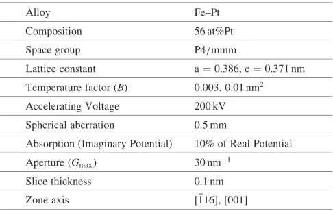
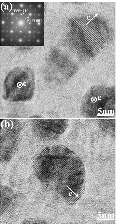
prolonged annealing at 873 K, the three-variant structural domains decomposed into single variant nanoparticles with their three possible directions of c-axes normal or parallel to the film plane.14) Figures 1(a) and (b) show the HREM images and the corresponding SAED pattern for Fe–56 at%Pt nanoparticles after annealing at 873 K for 86.4 ks. Single domain nanocrystal (single domain) particles are seen with their c-axes oriented both normal and parallel to the film plane, which results in an appearance of both 001 and 110 superlattice reflections in the SAED pattern with theh100i
incidence.
3.2 Evaluation of the order parameter
[image:2.595.306.549.83.237.2]We determined the order parameter using the intensities of 110 and 220 reflections. In the following, determination ofS
Table 1 Numerical parameters used for multi-slice calculations.
Alloy Fe–Pt
Composition 56 at%Pt
Space group P4/mmm
Lattice constant a = 0.386, c = 0.371 nm
Temperature factor (B) 0.003, 0.01 nm2
Accelerating Voltage 200 kV
Spherical aberration 0.5 mm
Absorption (Imaginary Potential) 10% of Real Potential
Aperture (Gmax) 30 nm1
Slice thickness 0.1 nm
Zone axis [1116], [001]
for this specimen is presented. A slight beam tilting from [001] incidence, for example, [1114] or [1116] incidence, results in an excitation ofhh0 systematic reflections, which reduces diffracted beams and can largely decrease and simplify the multiple scattering events among the transmitted and the diffracted waves. For [001] incidence, the intensity ratio I110=I220 shows complicated dependence of specimen
thickness even below 10 nm thick, while in the case of [1116] incidence, the intensity ratio increases monotonically. By tilting the specimen about 0.23 rad from the [001] incidence towards the [1¯10] direction, we can excite thehh0systematic reflections in the SAED pattern with beam incidence of [1116] as shown in Fig. 2. In the figure, the 110 and 220 reflection spots are indicated by the single arrow heads. The double arrow head indicates the 022 (and/or 202) reflection spot due to the existence of three kinds of c-axis orientation of the nanoparticles in the specimen. Since these reflections come from different particles with differentc-axis orientations and also these particles are two dimensionally distributed on the a-Al2O3 film, no phase relation exists, nor any double
diffraction occurs between these reflections. In Fig. 2, 220 reflections show slight arc along the circumference direction,
indicating a slight rotation of FePt nanoparticles on the substrate crystals. However, such a slight rotation on the substrate surface does not affect theI110=I220intensity ratio in
the case of [1116] incidence. The 110 and 220 intensities shown in Fig. 2 were measured as digital intensity data recorded in IP. The 220 and 202 (and/or 022) reflection profiles were separated by means of Lorentzian fitting. Here, a full width of half maximum (FWHM) of the 110 super-lattice reflection, 0.14 nm1, was used. The obtained intensity
ratio,I110=I220, was0:540:03.
In order to evaluate the order parameter for the present specimen, we need a relation between the calculatedI110=I220
ratio and the order parameter value. The relation on the basis of the multi-slice simulation is shown in Fig. 3 under the average particle thickness of 7 nm. Dotted line shows experimentally obtained I110=I220 value. Using the relation
Fig. 1 HREM images and the corresponding SAED pattern for Fe44Pt56
nanoparticles after annealing at 873 K for 86.4 ks. Nanoparticles withc -axis oriented normal and parallel to the film plane are seen in (a) and (b), respectively.
Fig. 2 A SAED pattern with beam incidence of [1116]. Excitation of thehh0 systematic reflections is seen. Besides the 110 and 220 reflection spots, 022 (and/or 202) reflection spot is also seen (indicated by double arrow head).
Fig. 3 Order parameter dependence of intensity ratioI110=I220obtained by
the multi-slice simulations. Solid and broken lines are the results obtained under the B values of 0.003 and 0.01 nm2, respectively. Dotted line
[image:3.595.69.269.70.457.2] [image:3.595.312.542.71.268.2] [image:3.595.324.525.555.729.2]in Fig. 3, the order parameter is determined as0:550:02. Then we examined the effect of thickness dependence on the order parameter. Particle thickness distribution was estimated to have a log-normal type distribution function with
ln¼0:39, which was assumed from the particle size distribution. Considering the above particle thickness dis-tribution, the average order parameter is expressed as follows:
S
S¼X
i
SðtiÞ nðtiÞ; ð2Þ
where SðtiÞdenotes the order parameter of the i-th particle
with the thicknessti andnðtiÞ the fraction of the thickness.
The summation was performed in the range of 71:5nm based on the deviation of ln¼0:39. Obtained average order parameter was 0.56, which is almost the same value as that of evaluated using an average thickness of 7 nm.
4. Discussion
The temperature factor used in this article was 0.003 nm2
both for Fe and Pt in the present multi-slice calculations. According to the International Tables for X-ray Crystallog-raphy,23) the Bvalues for bulk metals are tabulated, where
B¼0:0035 or 0.0018 nm2 for Fe and B¼0:0028 or 0.0022 nm2 for Pt at 293 K. Butt and Bashir24) presented a compilation of recommendedBvalues at 293 K. In their list,
B¼0:0035and 0.0032 nm2are presented for bulk Fe and Pt,
respectively. These are the bases for using theBof 0.003 nm2
in this study. In the assembly of FePt nanoparticles, the temperature factor may be different from that of the bulk FePt alloy due to the thermal vibration. There are several reports showing the increase of B with decreasing the particle size.25–31) Harada and Ohshima25) reported the temperature factor for Au particles, where theBvalue is about 0.01 nm2at
300 K for 15 nm-sized Au particles (B¼0:0062 or 0.0040 nm2,23)or 0.0057 nm224)at 293 K for bulk Au). They also showed that their obtainedBfor Au particles with sizes 6 to 23 nm included scarcely the static components. Ohshimaet al.26) reported the B of 0.0118 nm2 for 2-nm-sized Pd particles (B¼0:0032or 0.0036 nm2,23)or 0.0045 nm224)for bulk Pd). Kashiwaseet al.27)reported theBof 0.018 nm2for 3-nm-sized Cr particles (B¼0:002823)or 0.0026 nm224)
for bulk Cr). Crescenzi et al.,28) and Telgheder and Urban29) reported the size dependence of Bfor Cu clusters at 300 K, where obtained maximum value ofBwas about 0.01 nm2for
2-nm-sized clusters. In the present study, the mean particle size is 12 nm in diameter, so it is considered that the usedB
value of 0.003 nm2 is thought to be valid considering the
above results. We also calculated the intensity ratio under the largeBvalue of 0.01 nm2, and obtained theSof0:530:02
under the average particle thickness of 7 nm, which is 3.6% smaller than that of obtained by the calculation performed under theBof 0.003 nm2.
Present specimen of FePt nanoparticles showed a coer-civity of 434 kAm1 at 300 K14)after a sufficient annealing. Estimated saturation magnetization (Is) was 1.35 T using the averaged thickness of Fe and Pt which was monitored by quartz oscillator during the deposition. Here, we estimated the magnetoanisotropy constant at 300 K for the present FePt
nanoparticles as1:2{1:4106Jm3 based on the Pfeiffer’s equation32)assuming the random orientation of particles. The estimated magnetoanisotropy constant coincides in order with the values of FePt thin films6,7)with the order parameter of about 0.5. However, the estimated magnetoanisotropy constant includes not only magnetocrystalline anisotropy but also surface and/or shape contributions. Shima et al.15)
reported the decrease of anisotropy constant with decreasing the average FePt nanoparticle size. So it is concluded that the smaller nanoparticle sizes cause lower degree of order and reduce the magnetoanisotropy constant of the present FePt nanoparticles to give a smaller coercivity. Concerning the atomic ordering of FePt granular films, Takahashiet al.have recently discussed the decrease of the order-disorder trans-formation temperature with particle size.33)
5. Conclusion
Long-range order parameter of two-dimensionally distrib-uted Fe44Pt56 nanoparticles as small as 12 nm with
orienta-tion was determined as 0:550:02 by measuring electron diffraction 110 and 220 intensities from hh0 systematic reflections with the help of multi-slice intensity calculation under theBvalue of 0.003 nm2. Even by using theBvalue of
0.01 nm2, which is larger than that for bulk materials, the
order parameter decreased only 3.6%. From the coercivity and the saturation magnetization, we estimated the magneto-anisotropy constant to be 1:2{1:4106Jm3. The lower
degree of order and isolated small nanoparticles morphology are responsible for the relatively smaller Ku value of the present FePt nanoparticles compared with that of the bulk L10-FePt alloy. Determination of S by electron diffraction
has a great advantage for nanometer-sized materials, where conventional X-ray diffraction is thought to be difficult.
Acknowledgements
This study was supported by the Center of Excellence (COE) Program at ISIR-SANKEN, Osaka University, Grant-in-Aid for Scientific Research (Nos. 14205094, 13555189 and 13750612) and Special Coordination Funds for Promot-ing Science and Technology on ‘‘Nanohetero metallic materials’’ from the Japanese Ministry of Education, Culture, Sports, Science and Technology. This study was partly supported by Research Foundation For Materials Science.
REFERENCES
1) J. L. Dormann and D. Fiorani (ed.): Magnetic Properties of Fine Particles, (Elsevier, Amsterdam, 1992) pp. 93–177.
2) O. A. Ivanov, L. V. Solina, V. A. Demshila and L. M. Magat: Phys. Met. Metallogr.35(1973) 81–85.
3) D. Weller and M. F. Doerner: Annu. Rev. Mater. Sci.30(2000) 611– 644.
4) V. V. Maykov, A. Ye. Yermakov, G. V. Ivanov, V. I. Khrabrov and L. M. Magat: Phys. Met. Metallogr.67(1989) 76–82.
5) S. Mitani, K. Takanashi, M. Sano, H. Fujimori, A. Osawa and H. Nakajima: J. Magn. Magn. Mater.148(1995) 163–164.
6) H. Kanazawa, G. Lauhoff and T. Suzuki: J. Appl. Phys.87(2000) 6143–6145.
7) S. Okamoto, N. Kikuchi, O. Kitakami, T. Miyazaki, Y. Shimada and K. Fukamichi: Phys. Rev. B66(2002), 024413 1–024413 9.
8) B. E. Warren:X-ray Diffraction, (Dover, New York, 1990) pp. 208– 210.
9) C. P. Luo and D. J. Sellmyer: Appl. Phys. Lett.75(1999) 3162–3164. 10) S. Sun, C. B. Murray, D. Weller, L. Folks and A. Moser: Science287
(2000) 1989–1992.
11) Z. R. Dai, S. Sun and Z. L. Wang: Surf. Sci.505(2002) 325–335. 12) K. Sato, M. Fujiyoshi, M. Ishimaru and Y. Hirotsu: Scr. Mater.48
(2003) 921–927.
13) K. Sato, T. Kajiwara, M. Fujiyoshi, M. Ishimaru, Y. Hirotsu and T. Shinohara: J. Appl. Phys.93(2003) 7414–7416.
14) K. Sato, B. Bian, T. Hanada and Y. Hirotsu: Scr. Mater.44(2001) 1389–1393.
15) T. Shima, K. Takanashi, Y. K. Takahashi and K. Hono: Appl. Phys. Lett.81(2002) 1050–1052.
16) P. Hirsch, A. Howie, R. Nicholson, D. W. Pashley and M. J. Whelan: Electron Microscopy of Thin Crystals, (Krieger, Florida, 1977) pp. 90– 91.
17) K. Kaneko, S. Matsumura, K. Ikematsu, Y. Kato, Y. Tomokiyo, M. Watanabe and T. Masumoto: Scr. Mater.48(2003) 915–920. 18) P. M. J. Fisher: Jpn. J. Appl. Phys.7(1968) 191–199.
19) J. M. Cowley: Diffraction Physics, 3rd revised ed., (Elsevier, Amsterdam, 1995) pp. 189–253.
20) P. Buseck, J. M. Cowley and L. Eyring (ed.): High-Resolution Transmission Electron Microscopy and Associated Techniques,
(Oxford, New York, 1992) pp. 245–259.
21) B. Bian, K. Sato, Y. Hirotsu and A. Makino: Appl. Phys. Lett. 75
(1999) 3686–3688.
22) T. Oikawa, D. Shindo and K. Hiraga: J. Electron Microsc.43(1994) 402–405.
23) K. Lonsdale (ed.): International Tables for X-ray Crystallography, Vol. III (The Kynoch Press, Bermingham, 1962), pp. 232–244. 24) N. M. Butt and J. Bashir: Acta Cryst. A44(1988) 396–398. 25) J. Harada and K. Ohshima: Surf. Sci.106(1981) 51–57.
26) K. Ohshima, S. Yatsuya and J. Harada: J. Phys. Soc. Jpn.50(1981) 3071–3074.
27) Y. Kashiwase, I. Nishida, Y. Kainuma and K. Kimoto: J. Phys. Soc. Jpn.38(1975) 899.
28) M. De Crescenzi, M. Diociaiuti, L. Lozzi, P. Picozzi and S. Santucci: Phys. Rev. B35(1987) 5997–6003.
29) F.-W. Telgheder and J. Urban: J. Electron Spectroscopy and Related Phenomena95(1998) 267–279.
30) A. V. Chadwick, N. V. Russell, A. R. Whitham and A. Wilson: Sensors and Actuators B18–19(1994) 99–102.
31) J.-F. Lee, M.-T. Tang, W. C. Shih and R. S. Liu: Mater. Res. Bull.37
(2002) 555–562.
32) H. Pfeiffer: Phys. Status Solidi (a)118(1990) 295–306.
33) Y. K. Takahashi, T. Ohkubo, M. Ohnuma and K. Hono: J. Appl. Phys.