Absorbance Modulation Optical Lithography:
Simulating the Performance of an Adaptable
Absorbance Mask in the Near-Field.
John Foulkes
A thesis presented for the degree of Doctor of Philosophy
In
Electrical and Electronic Engineering at the
University of Canterbury, Christchurch, New Zealand.
A
BSTRACTThe challenge for lithography today is to continue the reduction of feature size whilst facing severe theoretical and practical limitations. In 2006 Rajesh Menon and Hank Smith proposed a new lithography system named absorbance modulation optical litho-graphy (AMOL) [Menon 2006]. AMOL proposed replacing the normal metal mask of a lithography system with an absorbance modulation layer (AML), made from a photoch-romic material. This allows, through the competition between two incident wavelengths, the creation of an adaptive absorbance mask. The AML allows intimate contact to an underlying resist and hence the optical near-field may be used to create sub-diffraction limited exposures. The aim of this thesis is to model AMOL and demonstrate the abili-ties and the limits of the system, particularly focusing on sub-diffraction limited imaging.
This thesis describes the construction of a vector electromagnetic simulation to explore the idea and performance of AMOL, and an exploration of the ability of AMOL to propagate sub-diffraction limited images into a photoresist. A finite element method (FEM) model was constructed to simulate the formation of apertures in the AML and light transmission through the system. Three major areas of interest were explored in this thesis; the effect of polarisation on imaging, using a plasmonic reflector layers (PRLs) to improve the depth of focus (DOF), and introducing a superlens to AMOL.
up to 60 nm and, although performance was reduced when using a silver PRL, the substantial improvements to the DOF and process latitude make a PRL valuable for an AMOL system.
This thesis also models the superlens to an AMOL system, which theoretically allows propagation of the image in the near-field. It is demonstrated that the superlens can project an AMOL image into an underlying resist, but that this image is degraded, especially for thick and non-ideal superlenses. The superlens does have a second useful effect, as it can act as a dichroic filter; decreasing the intensity ratio in the resist by a factor of ten, overcoming issues of resist sensitivity. The superlens can allow image projection and filtering with AMOL, however improvements to the available superlens materials or changes to the AML will be needed to avoid image deterioration.
P
REFACEThis dissertation describes research undertaken in the Department of Electrical and Computer Engineering at the University of Canterbury between March 2007 and De-cember 2010. I thank my supervisor, Professor Richard Blaikie for his suggestion of this topic of research and his continuous support of my work. The course of this thesis has been an interesting journey, combining the difficulties involved in creating and verifying a computer simulation of a novel lithography technique with the on-going challenges of near-field lithography.
Aspects of the work described in this dissertation have been published as follows:
Foulkes, JE & Blaikie, RJ 2009, 'Influence of polarization on absorbance modulated subwavelength grating structures', Journal of Vacuum Science & Technology B, vol. 27, no. 6, pp. 2941-6.
Foulkes, J & Blaikie, R 2008, 'Finite Element Simulation of Absorbance Modulation Optical Lithography', Melbourne, Australia: 2008, Proceedings International Confe-rence on anoscience and anotechnology (ICO 2008), Feb 25-29 2008, pp184-187
Aspects of the work described in this dissertation have been presented at the following conferences:
Oral Presentations:
Foulkes, J.E. and Blaikie, R.J. (2009) ‘Finite-element simulation of absorbance modula-tion optical lithography’. 4th International Conference on Advanced Materials and anotechnology (AMN-4), Dunedin, New Zealand, 8-12 Feb 2009
Foulkes, J & Blaikie, R 2008, 'Finite Element Simulation of Absorbance Modulation Optical Lithography', Melbourne, Australia: 2008, International Conference on anos-cience and anotechnology (ICO 2008), Feb 25-29 2008, pp184-187
Poster Presentations:
Foulkes, J.E. and Blaikie, R.J. (2009) ‘Influence of polarization on absorbance mod-ulated sub-wavelength grating structures’, 53rd International Conference on Electron, Ion, and Photon Beam Technology and anofabrication (EIPB), 26-29 May 2009. Marco Island, FL, USA
Aspects of the work described in this dissertation have been presented through the following seminars and talks:
Foulkes J & Blaikie, R, ‘Absorbance Modulation Optical Lithography with Plasmonic Reflectors’, Presentation to the anoLab users group, University of Canterbury, March 2010
Foulkes J & Blaikie, R, 2009, ‘Drawing at the Nanoscale’ Departmental Seminar, Department of Electrical and Computer Engineering, University of Canterbury, 29 May 2009
Foulkes J & Blaikie, R, 2008, ‘The challenges of nanometer resolution’, IET- Present around the world competition, University of Canterbury August 2008
PREFACE
A
CKNOWLEDGEMENTSFirstly I would like to thank my supervisor Professor Richard Blaikie for his support and guidance to my research over the course of this thesis. I would also like to acknowledge Rajesh Menon and Hank Smith for introducing the idea of AMOL and allowing me to visit MIT and discuss AMOL at the beginning of my research.
This thesis was undertaken at the Department of Electrical and Computer Engineering at the University of Canterbury and I would like to thank the department and all of the associated staff and students for their support. I would also like to thank the University of Canterbury Doctoral Scholarship for financial support of my thesis studies.
A special thanks to my fellow students who have shared in the battles of producing this thesis, in particular the other students in the lithography area: Mikkel Schøler, Ciaran Moore, Prateek Mehrotra and postdocs Trey Holzwarth and Matt Arnold. Your support, and the discussions at group meetings made my thesis better and the journey more interesting. Thank you also Mikkel, Ciaran and Prateek, along with David Kim, Jannah Ibrahim and, earlier, Jessica Chai for making the A217 office a relaxed but pleasant working environment; not forgetting those people who shared the slightly more hapha-zard arrangements in A219. Mikkel has shared both offices with me and has been a continuing presence during my thesis; I thank him for sharing the experience, for the many lunches at Tandoori Palace and stimulating discussions. I would also like to thank members of the wider MacDiarmid Institute, particularly those at the University of Canterbury, for exposing me to the many different areas encompassed by the phrase nanotechnology.
Andrew, Clare and Laura for lunchtime discussions at university, about research and other things.
T
ABLE OFC
ONTENTSChapter 1 ... 1
Introduction... 1
1.1 Motivation ... 1
1.2 Lithography ... 1
1.3 Alternative Techniques ... 7
1.4 Computational Lithography ... 10
1.5 Aims of this Thesis ... 11
1.6 Publications ... 12
Chapter 2 ... 15
Background ... 15
2.1 Introduction ... 15
2.2 Surface Plasmons ... 22
2.3 Measurement Metrics ... 24
2.4 Conclusions ... 27
Chapter 3 ... 29
Modeling of Photochromatic Layers ... 29
3.1 Introduction ... 29
3.2 Modeling Techniques ... 29
3.3 Modeling of Photoresists ... 30
3.4 Modeling of AMOL Photochromic Layers ... 35
3.5 Maxwell’s Equations ... 43
3.6 Intensity in Resist from Maxwell’s Equations ... 44
3.7 Vector and ScalAr Modeling ... 47
Chapter 4 ... 49
Modeling Methods ... 49
4.1 Motivation ... 49
4.2 Modeling Techniques ... 49
4.3 Finite Element Method Modeling ... 52
4.4 A Simple Example – Dielectric Boundary ... 55
4.5 Conclusions ... 61
Chapter 5 ... 63
FEM Modeling of AMOL ... 63
5.1 Introduction ... 63
5.2 AMOL Model in MATLAB ... 63
5.3 Plane Wave Incidence in AMOL ... 70
5.4 Photochromic Aperture Formation ... 73
5.5 Modeling an AMOL System ... 78
5.6 Full Comsol Model ... 80
5.7 Differences using A Vector Model ... 83
5.8 Conclusions ... 83
Chapter 6 ... 85
Polarisation effects ... 85
6.1 Introduction ... 85
6.2 Polarisation ... 86
6.3 Grating Modeling ... 87
6.4 Field Profiles Inside Gratings ... 94
6.5 Modeling Beneath Gratings ... 99
6.6 Light Profiles Beneath AMOL Gratings ... 107
6.7 Effect of Changing Period ... 114
TABLE OF CONTENTS
6.9 Formation of Narrow Apertures ... 117
6.10 Conclusions ... 120
Chapter 7 ... 123
Plasmonic Reflector Layers ... 123
7.1 Motivation ... 123
7.2 Depth of Focus ... 124
7.3 Plasmonic Reflector Layers ... 125
7.4 PRL in Absorbance Systems ... 129
7.5 Ideal PRL in AMOL ... 130
7.6 Effects of Introducing the PRL ... 141
7.7 Effect of Photoresist Depth ... 144
7.8 Silver PRL in AMOL ... 147
7.9 Conclusions ... 151
Chapter 8 ... 153
Plasmonic Transmission with AMOL ... 153
8.1 Motivation ... 153
8.2 Introduction to Superlensing ... 153
8.3 Superlensing in Absorbance Materials ... 161
8.4 Initial Simulation ... 163
8.5 A Silver Superlens ... 179
8.6 Conclusions ... 183
Chapter 9 ... 187
Conclusions and Future Work ... 187
9.1 Review of Thesis ... 187
9.2 Current AMOL Development ... 190
Appendix A - Units of Absorbance ... 195
Appendix B - Introduction to the Finite Element Method ... 199
Appendix C - Dielectric Boundary ... 207
Appendix D Matlab Code ... 211
L
IST OFF
IGURES1.1 Schematic of a proximity optical lithography process 3
1.2 Schematic of a projection optical lithography process 3
1.3 Evolution of projection optical lithography from 436 nm, 0.15 NA, 0.8 k1 to 193 nm immersion. The vertical bars represent the performance limits achieved with each technology; the shaded region represents the half wavelength limit [Lin
2006]. 5
1.4 ASML Twinscan XT:1950i scanner, a modern day lithography machine capable of imaging >140 wafers per hour. The illuminator (source), lenses, photomask
and stage (substrate) are labeled [French 2009] 8
1.5 Intensity of light passing through a metal ( = −4.4 − 18 ) aperture (width= 2 ) with wavelength (a) 0.5 nm and (b) 8 nm. At the short wavelength the light propagates with the diffractive orders visible, however the long wavelength only shows an evanescent field as the aperture is too narrow. 9
2.1 Principles of a STED fluorescence scanning microscope. An excitation beam and two offset STED beams are focused into the object for excitation and stimulated emission, respectively. The spontaneously emitted light is recorded in a (point)
detector. [Hell 1994] 17
2.2 Comparison the same crystal sections measured with (a) Confocal and (b) STED microscopy of densely packed nitrogen vacancy centres in diamond [Rittweger
2009] 17
2.3 Changing absorption spectra in a photochromatic material [Andrew 2009] 18
2.4 Isomerization of azo-compound causing photochromatic effect [Bouas-Laurent
2001] 19
2.5 Schematic of the AMOL procedure showing a single exposure using two standing waves and the ability to perform multiple exposure steps [Menon 2006]
2.6 Scanning electron micrographs of lines exposed in negative resist by AMOL system showing average linewidth of 117 nm. [Menon 2007] 20
2.7 Schematic of the Lloyd’s mirror configuration able to create a modulated and
plane-wave incident [Menon 2007] 20
2.8 Surface plasmon generation showing (a) generation of electric fields at the interface which create surface plasmons and (b) the dispersion curve showing the mismatch between the light line and surface plasmon [Barnes 2003]. 23
2.9 Demonstration of the and /2 points used to calculate the FWHM by finding thedistance between the two points where the intensity waveform crosses
/2. 25
2.10 Demonstration of the NILS metric showing slopes of the intensity waveforms measured at the desired linewidth, to be used in Eq 2.2. 26
3.1 Schematic of the interactions taking place in a photoresist layer, as described by Dill’s equations. The incident intensity, () decays due to three components, the inhibitor, reaction products and base resin, with the inhibitor transformed into
reaction products with fractional efficiency . 32
3.2 Actions of a contrast enhancement layer (CEL) showing (a) reduction of edges of exposure profile through CEL placed above resist [Kim 2007]. Demonstrating imaging performance without (b) and with (c) a CEL being used to fabricate 5 grating with 350-450 nm wavelength [Flack 2004]. 34
3.3 Showing the system used for the analytical analyses of AMOL. The axes are as and , with radial length , measured from the center of the exposure. The input intensity is , the depth of the photochromic layer is , with a matched substrate
below the resist removing all reflections. 37
3.4 Compression of the PSF achieved by AMOL system showing the ring illumination of , the incident PSF of and the compressed PSF after
transmission through the AML [Menon 2006]. 37
LIST OF FIGURES
three different cases (1,2,3) the ℐ at 8 beer lengths and the incident intensity ratio () (axis restricted to between 0 and 1). [Warner 2009] 41
3.6 Schematic demonstrating the volume, #, surface, $ and unit outward normal, %45
4.1 Cross section along y-axis of the analytical solution for the electric field intensity of a dielectric boundary at & = 0, between regions of with refractive indexes
( = 1 and ) = 2. 56
4.2 COMSOL simulation diagram showing (a) a sample intensity plot and (b) a
description of the geometry used. 57
4.3 Comparison of analytical solution (light blue) and COMSOL solution (black) to the dielectric boundary problem with (a) 65 elements, (b) 159 elements, (c) 470
elements and (d) 968 elements 59
4.4 (a) Coarse (65 elements) and (b) fine (3694 elements) COMSOL meshes for the
domain of the simple dielectric boundary problem. 60
4.5 Log axis plot of the Norm of the error between the analytical and COMSOL solutions plotted against the number of elements per wavelength area, a best fit
line is also plotted. 60
5.1 Chart showing operation of code to perform the simulation of a photochromic
layer in a FEM system. 64
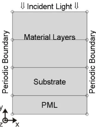
5.2 Schematic diagram showing the geometry and boundary conditions of the generic simulation. The substrate and PML were present in all simulations, however a variety of material layers were used, including an AML and photoresist and
possibly a plasmonic layer or air spacer layer. 66
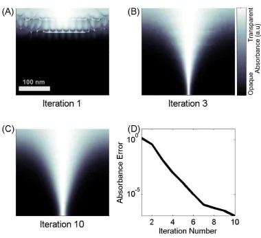
5.3 Absorbance pattern in the AML at iteration number (a) 1, (b) 3 and (c) 10, with
the measured change in absorbance plotted in (d). 70
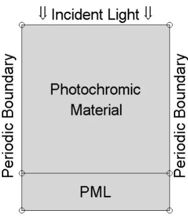
5.5 Schematic diagram showing the geometry and boundary conditions of the simulation of an infinite photochromic material. The absence of any substrate
layer means no reflections are modeled. 72
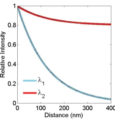
5.6 Comparison of analytical results (coloured solid lines) and COMSOL/MATLAB simulation (black dashed lines) over 400 nm for two plane wave incidence on an infinite AMOL material with no discernable difference seen at this magnification. The Beer length has been defined as 40 nm for with the Beer
length of a third of this. 72
5.7 Reproduction from Warner showing (a) Incident intensities for both wavelengths and (b) relative intensities at input, () and intensities at 8 Beer lengths into an infinite photochromic layer for three cases (, ); 1, (2.5, 5), 2, (2.5,10) and 3(3.1, 40), where ±0 are the peak positions of the Gaussian profiles [Warner
2009, split into two figures]. 73
5.8 Schematic diagram of FEM simulation used to create aperture profiles in an infinite photochromic layer showing the incident wavelengths, photochromic
layer and PML. 74
5.9 Aperture formation of a photochromic system for TE case using the FEM model (coloured) with analytical solutions overlaid in dashed black lines showing strong
agreement. 74
5.10 Aperture formation of a photochromic system for TE case using the FEM model (coloured) with analytical solutions overlaid in dashed black lines showing some agreement. The effect of polarisation is noted as there is increased transmission in the TM case, and hence disagreement with the scalar methods. Here u is the
depth (in nm) into the photochromic layer 76
5.11 (a) Comparison of FEM and analytical aperture formation of a photochromic system for TE case where the aperture size is narrower than the wavelength. (b) Talbot effect seen in the intensity in the photochromic layer from the FEM system. This is present because there is only a short aperture created before an approximately constant absorbance is seen due to absorbance of . 77
LIST OF FIGURES
subsequently by (b) 20 mW/cm2 at 546 nm. The experimental data (solid) are overlaid with the simulation (dashed), which enables the extraction of the photochromic parameters listed beneath the diagram. [Menon 2007] 79
5.13 Normalised Intensity with distance into the photoresist from the FEM model of a photochromic layer. The dotted lines show the intensity at 200 nm, as used for the comparison with an analytical solution. The intercepts are at normalised
intensities of 0.067 and 0.0058. 81
5.14 Schematic diagram showing the geometry and boundary conditions of the
simulation of for the initial full AMOL system. 81
5.15 Typical simulation result, showing only absorbance in the photochromic layer and the intensity of in the photoresist. This simulation has a relatively large 1000 nm period and hence the propagation into the resist is strong. 82
5.16 FEM simulation of (a) TM and (b) TE polarized light showing the absorbance in the AML (above the line at & = 0) and the light intensity propagated into the resist (below the line at & = 0) at an input intensity ratio ()/() = 1.35. The standing-wave and plane-wave illumination schemes at and , respectively, are shown schematically at the top of each figure. 83
6.1 The axes used in this work and the separation of the electric and magnetic fields
for TE and TM polarisation. 87
6.2 Schematic diagram of the AMOL process being modeled 88
6.3 Analytic grating model demonstrating the model geometry, variables and coordinate system with infinite extent in the third dimension. 89
6.4 Plots showing the intensity profiles predicted by a Rytov Analysis for (a) . and (b) /0for transmission in an 80 nm grating consisting of a dielectric (Region 1, 1 = 4) and an air gap (Region 2, 1 = 1) and wavelength of 436 nm. The absolute value of the intensity is arbitrarily chosen but allows fair comparison
between (a) and (b). 92
6.5 FEM grating model showing air gap, grating and photoresist layers for a 140 nm period grating; illuminated from above with polarised as TE or TM as shown
6.6 Light intensity relative to input field inside 50% duty cycle, 80 nm pitch gratings for TM and TE polarised light at 436 nm for (a) Metal (Nichrome), (b) dielectric and (c) strongly absorbing gratings with FEM simulation. The crosses mark TE results of the Rytov model results for the same cases. 95
6.7 Two-norm of the difference between the waveform calculated by the FEM and Rytov models of (a) metal and (b) absorbing gratings as the grating period is increased. The incident wavelength is 436 nm. The apparent poor agreement in TE polarisation is due to a disagreement in field strength rather than waveform profile, suggesting that the relative field strengths are incorrect in the Rytov
model.. 95
6.8 Grating waveforms for a 200 nm period, 50% duty-cycle grating between air
(= 1) and an increasing absorbing medium. 97
6.9 Comparison of metal (1= -13.24 − 14.624) and absorbance (1 = 1 − 34) gratings as the period increases past the incident wavelength. Grating images are shown at (a) 200 nm, (b) 400 nm and (c) 2000 nm, with an incident wavelength
of 436 nm. 98
6.10 Intensity waveforms for a 120 nm period absorbance grating (1 = 1 − 24, right hand side) when the portion which is less absorbing (1 = 1, left hand side)
increases from 25% – 50% – 75%. 100
6.11 Light intensity after passing through (a) metal and (b) absorbance gratings with 80 nm period and 50% duty cycle, as calculated using FEM simulations. Horizontal intensity profiles are taken inside the grating, at the exit, 20 nm, and
50 nm beneath the grating. 103
6.12 Comparison of FEM and analytical methods for modeling the propagation of electromagnetic fields beneath waveforms; (a) is based on a Rytov grating and (b) on the FEM calculated field profile at the base of the grating. 105
6.13 Contrast as a function of depth below the grating for (a) 200 nm and (b) 20 nm period gratings. Solid and dashed lines represent absorbing and metal gratings
LIST OF FIGURES
6.14 Plot of the contrast depth of focus FEM simulations of 50% duty cycle absorbance-modulated and metal gratings as the period is increased from 0 to
200 nm. 106
6.15 Comparison of standing waves formed by TE and TM polarisations, with (a) showing electric field diagram and (b) demonstrating the difference in intensity
profile when the angle is 200. 109
6.16 FEM simulation of TE polarized 1 light showing the absorbance in the AML (above the line at & = 0) and the light intensity propagated into the resist (below the line at & = 0) at an input intensity ratio ()/() = 1.35. The standing-wave and plane-standing-wave illumination schemes at and , respectively, are shown
schematically at the top of the figure. 110
6.17 FEM simulation of TM polarized 1 light showing the absorbance in the AML (above the line at & = 0) and the light intensity propagated into the resist (below the line at & = 0) at an input intensity ratio ()/() = 1.35. The standing-wave and plane-standing-wave illumination schemes at and , respectively, are shown
schematically at the top of the figure. 110
6.18 (a) intensity in the first 50 nm of resist for TE polarised light with an input intensity ratio ()/() = 1.35. Intensity profiles are shown at (b) 0 nm, (c)
25 nm and (d) 50 nm below the AML. 111
6.19 (a) intensity in the first 50 nm of resist for TM polarised light with an input intensity ratio ()/() = 1.35. Intensity profiles are shown at (b) 0 nm, (c)
25 nm and (d) 50 nm below the AML. 111
6.20 The FWHM of (a) the AMOL aperture and (b) the intensity profile at the base of the AML in the FEM simulation as the input intensity ratio ()/() is
varied to change the aperture size. 113
6.21 The (a) contrast and (b) DOF of TM and TE polarised as the input intensity ratio ()/() is varied to change the aperture size. 114
6.22 Comparison of the (a) contrast and (b) DOF for TE and TM polarised transmission performance as the period of the λ2 standing wave in the AMOL
6.23 (a) intensity in the first 50 nm of resist for TM polarised light with intensity profiles shown at (b) 0 nm, (c) 25 nm and (d) 50 nm below the AML
demonstrating a frequency doubling effect. 115
6.24 Comparison of the intensity waveforms produced by TM and TE polarised 1 when the period of the standing wave is (a) 100 nm, (b) 200 nm and (c)
290 nm. 116
6.25 Showing the effect of reducing the duty cycle for TM polarised light, as measured by the FWHM of the (a) resist intensity waveform and the (b) base of
the AML, for a 400 nm AMOL system. 117
6.26 (a) Maximum Contrast and (b) Minimum FWHM achieved in an AMOL system with changing chromophore density. A minimum FWHM of 24 nm is achieved ((thermal constant 8.5 × 10 − 9 to remove any thermal effect). 119
6.27 (a) Maximum Contrast and (b) Minimum FWHM achieved in an AMOL system with changing thermal constant density. Limited further improvement in performance is seen when the thermal constant is reduced below 2 × 10 − 4 78.
119
7.1 Schematic of the AMOL process being modeled including plasmonic reflector
layer (PRL). 124
7.2 Comparison of an ENFOL system with and without a near-field plasmonic layer (NFPL) demonstrating improved confinement in resist. Intensity profiles for 140 nm period Cr gratings illuminated at 365 nm with (a) an index matched
substrate and (b) a silver NFPL. [McNab 2004] 126
7.3 COMSOL simulation of Photoresist exposures for rectangular metal gratings without (a) and with (b) a plasmonic reflector layer. The gratings are 50% duty-cycle, 100 nm period gratings, modeled at 400 nm with 50 nm of photoresist (n = 1.6 − 0.05j, ϵ< = 2.5575 − 0.16i) and either a matched layer or plasmonic layer (ϵ< = −2.5575 − 0.16i), both semi-infinite. The grating material has permittivity of ϵ< = 4.4 − 18i and 1. 126
LIST OF FIGURES
(but representative) image with no reflection is shown in (a) and with reflection
(b). [Arnold 2007] 127
7.5 Photoresist exposures replicating Fig 7.3 for rectangular absorbance gratings without (a) and with (b) a plasmonic reflector layer. The gratings are 50% duty-cycle, 100 nm period gratings, modeled at 400 nm with 50 nm of photoresist ( = 1.6 − 0.05 , = 2.5575 − 0.164) and either a matched layer or plasmonic layer ( = −2.5575 − 0.164), both semi-infinite. The absorbance
grating has permittivity of = 1 − 3 and 1. 130
7.6 AMOL absorbance and intensity in the photoresist for AMOL system with (a) matched substrate and (b) an ideal PRL beneath a 50 nm photoresist. The best case results based on NILS are shown which occurred at an / intensity ratio
of (a) 19 and (b) 15. 132
7.7 The intensity in the resist for an AMOL system with a matched substrate (a) and normalised (to ) intensity waveforms at (b) 0 nm, (c) 25 nm and (d) 50
nm beneath the AML layer. 133
7.8 The intensity in the resist for an AMOL system with an ideal PRL (a) and normalised (to ) intensity waveforms at (b) 0 nm, (c) 25 nm and (d) 50 nm
beneath the AML layer. 133
7.9 Comparison of the maximum and minimum NILS (a,b) and FWHM (d,c) between an AMOL system with a matched layer behind 50 nm of photoresist and a system with 50 nm photoresist followed by semi-infinite ideal reflecting layer. Plots show the results as the input intensity ratio is varied, producing different
absorbance profiles. 135
7.10 Comparison of the maximum intensities of (a) , (b) and (c) / between an AMOL system with a matched substrate or a semi-infinite ideal PRL behind 50 nm of resist as the input intensity ratio is increased. 136
7.11 Linewidths with depth into photoresist from base of AMOL for (a) index matched substrate and (b) ideal PRL substrate, at 0.2 × , 0.3 × and 0.4 × in both pictures. is defined as maximum intensity in top
7.12 AML absorption in the best case matched substrate AMOL system (a). Absorbance is represented by the imaginary refractive index, ?, ranging from 0 to -2.2. Horizontal absorbance waveforms are shown at (b) 80 nm, (c) 150 nm and
(d) 200 nm. 139
7.13 AML absorption in the best case AMOL system with PRL (a). Absorbance is represented by the imaginary refractive index, ?, ranging from 0 to -2.2. Horizontal absorbance waveforms are shown at (b) 80 nm, (c) 150 nm and (d)
200 nm. 139
7.14 Aperture width against depth into AML for matched substrate and for an AMOL
system with an ideal PRL after 50 nm of resist. 140
7.15 Comparison of the four cases for the intensity ratios / giving the best NILS showing (a) A and (b) B from previous considered cases and the fictitious (c) C( has a PRL, matched substrate) and (d) D ( has a matched substrate, a PRL) showing the absorbance in the AML and the intensity in the
photoresist. 142
7.16 Comparing the changes in NILS (a) and FWHM (b) for a PRLs placed at changing depth beneath the AML. Also included for comparison is the best NILS and FWHM performance of an AMOL system with a matched layer. The reason for the kink at 60 nm is unknown but it does not indicate an improvement in the
confinement of . 146
7.17 intensity in the resist for an AMOL system with an ideal PRL at 15 nm beneath the AML (a) and normalised (to ) intensity waveforms at (b) 0 nm,
(c)7 nm and (d)15 nm beneath the AML layer. 146
7.18 AMOL absorbance and intensity in the photoresist for silver PRL in an
AMOL system separation of 50 nm 148
7.19 The intensity in the resist for an AMOL system with a silver PRL (a) and normalised (to ) intensity waveforms at (b) 0 nm, (c) 25 nm and (d) 50 nm
beneath the AML layer. 148
LIST OF FIGURES
8.1 (a) Refraction at a boundary between two media and (b) focusing by a planar
negative index slab [Vesalego 1968] 155
8.2 AFM images of gratings imaged through a 25 nm/50 nm/10 nm – PMMA/Ag/SiO2 lens stack, with periods of (d) 250 nm, (e) 200 nm, (f) 170 nm
[Melville 2005] 160
8.3 Comparison of the effect of introducing a superlens showing (a) an focused ion beam image of an arbitrary object “NANO” with 40 nm linewidth (b) the image result with silver superlens, (c) the image result with silver superlens replaced by PMMA spacer and (d) the average cross-section of letter A. [Zhang 2005] 160
8.4 Intensity profiles at 400 nm created in a system without (a,c) and with (b,d) a 30 nm superlens with 10 nm spacer into a system with 100 nm gratings of (a,b) metal ( = −4.4 − 18 )/air (= 1) and (c,d) absorber(= 1 − 3 )/ air
(= 1). 162
8.5 Schematic diagram of the AMOL system with included superlens. The superlens
may include an additional spacer layer. 163
8.6 Absorbance in the AML and intensity in the resist layer for an AMOL system with (a) the resist with a matched substrate directly beneath the AML and (b) with a 30 nm superlens directly between the AML and resist with matched
substrate 165
8.7 (a) Intensity profile for the transmission of 50 nm beneath an AMOL system with matched substrate. Intensity profiles relative to are shown at (b) 0 nm,
(c) 25 nm and (d) 50 nm depths. 166
8.8 (a) Intensity profile for the transmission of 50 nm beneath an AMOL system with 30 nm ideal superlens sandwiched between the AML and resist with matched substrate. Intensity profiles relative to are shown at (b) 0 nm, (c)
25 nm and (d) 50 nm depths. 166
8.9 Absorbance in the AML and intensity in the resist layer for an AMOL system and one with a 10 nm spacer layer and 30 nm superlens directly between AML
8.10 (a) Intensity profile for the transmission of 50 nm beneath an AMOL system with 10 nm spacer layer and 30 nm ideal superlens sandwiched between the AML and resist with matched substrate. Intensity profiles relative to are shown at (b) 0 nm, (c) 25 nm and (d) 50 nm depths. 167
8.11 Affect on (a) NILS and (b) FWHM of increasing the spacer thickness for a 30 nm
superlens. 168
8.12 (a) Intensity profile for the transmission of 50 nm beneath an AMOL system with a 60 nm ideal superlens sandwiched between the AML and resist with matched substrate. Intensity profiles relative to are shown at (b) 0 nm, (c)
25 nm and (d) 50 nm depths. 169
8.13 (a) NILS and (b) FWHM measured with photoresist depth for the intensity profile shown in Fig 8.12 demonstrating a focusing effect occurring at a depth of
~60-70 nm. 169
8.14 Effect of changing superlens depth on the transmission of as measured by (a)
NILS and (b) FWHM 171
8.15 Comparison of the maximum and minimum NILS (a,b) and FWHM (d,c) between AMOL systems with and without a 15 nm ideal superlens with 10 nm spacer layer as the incident intensity ratio / is varied 171
8.16 AML absorbance and resist intensity plots for the best case NILS AMOL system and an AMOL system with a 10 nm spacer layer and 15 nm superlens directly
between AML. 172
8.17 (a) Intensity profile for the best NILS case for transmission of 50 nm into a resist layer by an AMOL system with a 10 nm spacer and 15 nm ideal superlens sandwiched between the AML and resist with matched substrate. The intensity profiles are relative to in the resist and are shown at (b) 0 nm, (c) 25 nm
and (d) 50 nm depths. 174
8.18 (a) Intensity profile for the best NILS case for transmission of 50 nm into a resist layer by an AMOL system with a matched substrate. The intensity profiles are relative to in the resist and are shown at (b) 0 nm, (c) 25 nm and (d)
LIST OF FIGURES
8.19 Comparison of the maximum intensities of (a) , (b) and (c) / between an AMOL system with a matched substrate and an AMOL system with an ideal 15 nm superlens ( = −2.775 − 0.164) with 10 nm spacer. 176
8.20 (a) AML absorption in the best NILS case for a matched substrate AMOL system. Absorbance is represented by the imaginary part of the refractive index, ?, ranging from 0 to 2. Horizontal absorbance profiles are shown at (b) 80 nm (c)
150 nm and (d) 200 nm into the AML 178
8.21 (a) AML absorption in the best NILS case for an AMOL system with a 15 nm ideal superlens and 10 nm spacer. Absorbance is represented by the imaginary part of the refractive index, ?, ranging from 0 to 2. Horizontal absorbance profiles are shown at (b) 80 nm (c) 150 nm and (d) 200 nm into the AML 178
8.22 (a) NILS and (b) FWHM for as the thickness of a silver superlens is increased
(at 405 nm) 180
8.23 (a) Intensity profiles having the best NILS for transmission of 50 nm beneath an AMOL system with a 10 nm spacer and 10 nm silver superlens sandwiched between the AML and resist. Intensity profiles relative to are shown at (b)
0 nm, (c) 25 nm and (d) 50 nm depths. 180
8.24 (a) Intensity profiles having the best NILS for transmission of 50 nm beneath an AMOL system with a 10 nm spacer and 15 nm silver superlens sandwiched between the AML and resist. Intensity profiles relative to are shown at (b)
0 nm, (c) 25 nm and (d) 50 nm depths. 180
8.25 (a) Intensity profile for the best NILS case for transmission of 50 nm beneath an AMOL system with a 10 nm spacer and 15 nm silver (at 365 nm) superlens sandwiched between the AML and resist with matched substrate. Intensity profiles relative to are shown at (b) 0 nm, (c) 25 nm and (d) 50 nm depths.
181
8.26 Comparison of the maximum intensities of (a) , (b) and (c) / between an AMOL system with a matched substrate and an AMOL system with an silver type, 15 nm superlens (, = −2.6 − 0.44, ; , = −12.6— 0.424) and 10
9.1 intensity in the resist for an AMOL system with an ideal PRL at 15 nm beneath the AML (a) and normalised (to ) intensity waveforms at (b) 0 nm,
(c) 7 nm and (d) 15 nm beneath the AML layer. 191
B.1 Basis functions for a 2-Dimensional triangular finite element, with the function
defined as zero anywhere outside the element. 203
L
IST OFT
ABLES5.1 Parameter values calculated for AMOL, based on values published by Menon [Menon 2007] and measured by Holzwarth [Holzwarth 2010] with conversions into
A
CRONYMS ANDA
BBREVIATIONSAMOL Absorbance Modulation Optical lithography
AML Absorbance Modulation Layer
ArF Argon-Fluoride Laser
CEL Contrast Enhancement Layer
DE Differential Equation
DFT Discrete Fourier Transform
DOF Depth of Focus
EBL Electron Beam Lithography
EFOL Enhanced Near-Field Optical Lithography
EUV Extreme Ultraviolet Lithography
FDTD Finite Difference Time Domain
FEM Finite Element Method
FTIR Frustrated Total Internal Reflectance
FWHM Full Width at Half Maximum
ITRS The International Technology Roadmap For Semiconductors
i/j Imaginary Unit
LSF Line Spread Function
A Numerical Aperture
ILS Normalised Image Log Slope
OPC Optical Proximity Correction
PML Perfectly Matched Layer
PRL Plasmonic Reflector Layer
PMEA poly[4-[2-(methacryloyloxy)ethyl] azobenzene]
RET Resolution Enhancement Techniques
RCWA Rigorous Coupled Wave Analysis
STED Stimulated Emission Depletion Microscopy
SERS Surface Enhanced Raman Spectroscopy
SPECL Surface Plasmon Enhanced Contact Lithography
TE Transverse Electric
TM Transverse Magnetic
Chapter 1
ITRODUCTIO
1.1
MOTIVATIO
Lithography is of central importance to the construction of any small features, with particular relevance to the semiconductor industry. Advancements in lithography allow new generations of improved microchips and improved development processes. If it is desired to continue the exponential increase in computing power of the last forty years then lithographic improvements will be necessary.
The constant technological development in lithography engineering has led to consider-able variety in and complexity of the techniques used to pattern at scales from micrometers down to nanometers. In this thesis a lithography technique involving the optical near-field and the use of an absorbance-modulated mask are the primary focus, investigating and characterising these techniques through modeling and exploring the possibilities for improving their performance. The techniques developed here are not mainstream industrial techniques, but promise interesting advantages when considering the obstacles facing lithography’s ongoing development, alongside the possibility to explore the details of how light may be confined to form sub-wavelength features.
1.2
LITHOGRAPHY
industry-created requirement to increase the functionality of devices whilst reducing size, failure rate and cost and improving yield has led to intensive efforts to scale the feature sizes of integrated circuits to smaller dimensions. The continued development of optical lithog-raphy technologies [Lin 2006, Fay 2002] has enabled these goals to be achieved and optical lithography has remained the mainstream method for integrated chip production since the inception of the industry. In the past when it has been assumed that a feature size limit was reached, new developments and techniques have allowed the further reduction of feature sizes from the micrometer range to current integrated circuits with critical dimensions of less than 40 nm.
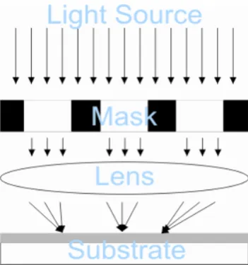
Although early optical lithography techniques began as optical printing, involving masks in contact or close proximity (Fig 1.1) the general industry trend has been towards optical projection lithography as this reduces the difficulties with mask contamination [Ronse 2006]. The basic structure of a projection system used for optical lithography takes the light from the laser source, passes it through a beam expander, before it im-pinges on a mask. The light pattern is then focussed by an objective/projection lens onto a photoresist layer on the wafer, as shown in Fig 1.2. In order to improve the image resulting from the lithography system adjustments may be made to each of the compo-nents: different photoresist selection may allow for improved selectivity, improved construction of the lenses and masks can decrease the presence of defects and a more ideal light source can reduce secondary effects like dispersion. After the image has been transferred into the photoresist a development of the photoresist must take place to produce the desired feature, the details of this process will depend heavily on the nature of the resist used as well as the quality of the transferred image.
1.2.1
PROJECTIO LITHOGRAPHY
1.2 LITHOGRAPHY
[image:35.595.230.408.109.228.2] [image:35.595.230.406.259.447.2]requirement and combines a variety of factors including maximum throughput, exposure speed, availability and expense of required materials and the ability to produce on a large scale. The lithographic effectiveness may be represented by the resolution of the system, which Mack defines as the smallest feature that can be reproduced with adequate control [Mack 2007]. The maximum resolution achievable by any optical lithography system is inherently important because it sets the smallest possible linewidths that can be drawn using the particular lithographical processes and hence the maximum number of transis-tors in any given area.
The resolution of a given projection optical lithography system may be related to the wavelength, and numerical aperture, IJ of the system by the Rayleigh equation
Figure 1.1 Schematic of a proximity optical lithography process
E = KIJ (1.1)
where K is the merit factor of the lithography system [Mack 2007]. This equation arises from a definition of loss in resolution as the point at which two point spread functions are brought together such that the peak of one overlaps the first diffractive order of the second. A second important measurement parameter is the depth of focus (LMN – also known as depth of field), for a projection system this is a measure of the depth for which an adequate focus for imaging can be achieved in the resist. For a grating of equally spaced lines this may be approximated by the relation
LMN = KIJ, (1.2)
where K is a system constant, although this expression requires several caveats and may be of limited accuracy [Mack 2007]. It is desirable to produce a smaller resolution and larger LMN; it may be seen from Eqs 1.1 and 1.2 that by decreasing either K, or increasing IJ a smaller and hence improved resolution may be achieved. However reducing or increasing IJ causes a reduction in the LMN and hence more difficult development process and smaller process latitude.
The reduction of wavelength in order to achieve improved resolution has led from the use of the g-line of a mercury lamp at 436nm in the 1980’s to the use of lasers such as Argon-Fluoride (ArF) at 193 nm in current production systems (Fig 1.3). Although continued reduction of the wavelength used in the optical system would result in im-proved resolution capabilities numerous challenges have arisen. A change in wavelength requires each section of the optical lithography system to be redesigned; a new photore-sist absorbing at the wavelength must be chosen and the lens materials must be carefully selected to avoid absorption and overheating.
1.2 LITHOGRAPHY
and too much absorbance in resists [Lin 2006]. This has forced research into improving the performance of material parameters [Sanders 2010] and resolution enhancement techniques (RET) [Mack 2007, Trouiller 2006] at 193 nm. Alongside the introduction of new experimental techniques the increasing use of simulations and computational methods has enabled the testing of new ideas and a greater understanding of the proc-esses taking place [Mack 2006, Cole 2001, Mack 2001].
The numerical aperture of the system is a measure of the ‘light gathering ability’ of the lens in the lithography system, it is a product of the refractive index () and the angular semi-aperture (O) in the object space;
IJ = × 74(O). (1.3)
Through complex lens design and material choice the numerical aperture of the system may be increased, however because of the square in Eq 1.2 this can lead to a large and undesirable reduction in LMN. A major breakthrough in IJ improvement was made with the implementation of immersion lithography [French 2009, Ronse 2009, Bratton 2006] in which the volume between the lens and the wafer is filled with a fluid with higher refractive index than air (e.g water) that will act to increase the IJ of the lens; this is particularly impressive given that the lithography system is moving rapidly to
sweep across the wafer, and the engineering of such systems now needs a strong under-standing of hydraulics and fluid dynamics in additional to the optical design.
The final component of the resolution equation is the merit factor, K, of the optical lithography system. This is used to describe the effects of changing system parameters and features, such as the resist process, resolution enhancement techniques (RET) or optical proximity correction (OPC) [Mack 2007]. There is an extensive selection of techniques which have been investigated to lower the Kof a lithography system such as phase shifting masks, off-axis illumination and polarization [Ronse 2006]. Each of these requires additional machinery, understanding and process steps, however the demand for resolution improvement continues to encourage further developments in these areas [Pease 2008]. The K value has a theoretical limit for dense half-pitch gratings of 0.25, although the manufacturable limit may be higher [Lee 2009]. With current technologies already requiring reduction from ~0.5 to ~0.30 further improvements are even more challenging.
1.2.2
CURRET LITHOGRAPHY SYSTEMS
The International Technology Roadmap For Semiconductors (ITRS) is a industry led group whose main aim is to “present industry-wide consensus on the ‘best current estimate’ of the industry’s research and development needs out to a 15-year horizon” [ITRS 2009]. The 2009 roadmap outlined the current technology involved in creating 45 nm half-pitch DRAM, using a 193 nm wavelength from an ArF laser with water immersion, a K value 0.28-0.31 and making use of a variety of corrective techniques including OPC. Thus using Eq 1.1
Resolution = K∗NA ≈ 0.31 ∗λ 1.35 = 44nm,193 (1.4)
with a reducing LMN for a single layer resist of
LMN = K∗NAλ ≈ 1 ∗1.35193 = 105nm, (1.5)
1.3 ALTERNATIVE TECHNIQUES
Moore’s law [Moore 1998] is to continue then so must further improvements, the ITRS report notes that no proven optical technique exists below 22 nm, ~/9 for the 193 nm wavelength. The struggle for further improvement and the complex nature current optical projection lithography systems (Fig 1.4) has also inspired a search for alternative techniques that can improve the resolution and match the speed of current projection lithography.
1.3
ALTERATIVE TECHIQUES
The techniques of double patterning and self-assembly lithography give options to extend the reach of current technologies. For instance double patterning (possibly followed by triple and/or quadruple patterning) allows the same optical lithography techniques to be used but requires additional process steps, either extra development and re-exposure or protection of the first exposure; these additional steps increase the time taken for the fabrication process as well as the importance of accurate alignment. Simi-larly self-assembly lithography processes increase the complexity of the lithographical systems because the operation of the introduced self-assembly compounds and their relation with the lithographical systems must be well understood. The advantage of these methods, that they build upon previous optical lithography methods, is also partially shared by the small wavelength methods.
The small wavelength methods (x-ray, EUV and EBL) take advantage of their much smaller wavelengths to avoid diffraction effects; this will allow better resolution [Stulen 1999] but two major problems exist. Firstly there is a materials problems: at short
[image:40.595.142.413.112.347.2]1.3 ALTERNATIVE TECHNIQUES
wavelengths it is no longer possible to design refractive lenses due to absorption, hence reflective mirrors must be used and although advances have been made this remains problematic; alongside this are mask and resist problems [Wurm 2009]. Secondly it has proven difficult to develop high power, high resolution, sources, for this reason EBL has remained a single beam, non-masked lithography which is inherently slow, well below the speed required for large scale manufacture (but widely used for laboratory and small scale work) and research has focused on developing improved power sources at EUV. Each of these techniques have strong performance possibilities which has encouraged large investment and research, however the discussed obstacles remain before they can take over from projection lithography systems.
Another alternative technique to overcome the diffraction limit problem is to make use of the optical near-field. Projection lithography works with propagating light at large distances and hence undergoes diffraction after passing through, say a narrow aperture (Fig 1.5a), but continues to propagate (hopefully towards a lens). If the aperture is narrower than /2 it may be shown that an evanescent field is produced in the region just behind the aperture and that these evanescent waves contain the complete spatial information but decay exponentially (Fig 1.5b). It was shown [McNab 2001] that
non-Figure 1.5 Intensity of light passing through a metal (= −4.4 − 18 ) aperture (width= 2 ) with
diffraction limited lithographical systems are possible in this region, although the decay is dependent on spatial frequency and hence non-uniform and the exponential nature of the decay requires that the mask and photoresist are placed as close together as possible, leading to contact issues and contamination problems.
Combining the optical near-field with a technique to control and reduce the exposure size would allow non-diffraction limited lithography and have been explored by tech-niques such as beam-pen lithography [Huo 2010] in which a gold covered polymer tip is used to guide light to a narrow aperture. Instead of requiring the fabrication of such a system or the creation of a similar near-field source it would be much preferable to use far-field sources as these are commonly available and simple to use. An implementation of this idea was suggested by Hell [Hell 2004, Hell 2003] following on from work in stimulated emission depletion microscopy (STED) involving two competing incident wavelengths with a third input used to ‘freeze’ the final form when desired. Although this idea was not directly used it inspired a series of related non-linear far-field enabled near-field systems which may enable nanoscale lithography with visible light sources [Fourkas 2010]. These include two-color excitation/deactivation photolithography [Scott 2009] and absorbance modulation optical lithography (AMOL). AMOL combined the possibilities of using the optical near-field and double patterning without multiple development stages [Menon 2007] through the use absorbance modulation layer (AML) as a mask. AMOL is an exciting idea because it proposes access to the advantages of both of these alternative techniques as well as remaining within the technological area of projection lithography and it is the subject of the majority of this thesis.
1.4
COMPUTATIOAL LITHOGRAPHY
1.5 AIMS OF THIS THESIS
theoretical understanding of each section of lithographical systems and the need for lithographers to be able to test improvements [Mack 2006] it has since been necessary to develop ever more complex computational methods to explain the interactions between light, chemicals, fluids and movements taking place.
The Dill papers [Dill 1975, Dill 1975a, Dill 1975b] introduced a linear model for photo-resist exposure and development and mark the start of the computational lithography. Since these early models many more assumptions have been removed, for instance; high IJ systems requiring vector models to replace scalar models, small dimensions requir-ing differentiation between polarizations, and stochastic modelrequir-ing to determine and reduce variations and improve process latitude. For modern systems every part of the lithography process is relentlessly optimized, either with complex models or through simulations; the difference between the mask pattern and the images formed has led to optical proximity correction (OPC) in which the mask is adjusted to create an improved image; the illumination can similarly be adjusted to optimize performance. Computa-tional simulation is a mainstay of the lithography industry today; its performance in areas of research, optimization and understanding has allowed the improvements in resolution seen today [Mack 2006, Cole 2001, Mack 2001]. Of course, there must always be a combination of the computational work with experimental results, allowing each method to push the other forward and encourage new ideas.
1.5
AIMS OF THIS THESIS
This thesis begins with a review of the development of modeling in lithography leading towards the creation of a model of a photochromic system. This chapter is followed by the presentation of background material introducing AMOL and surface plasmon. After the background in introduced the next two chapters introduce the modeling of photoch-romic layers and resists and validate the FEM modeling of Maxwell’s equations, describing the transmission of light in an optical system. The FEM model of the AMOL system is described and validated in full in the fifth chapter completing the model development stage. The later chapters explore the interaction of AMOL with known near-field effects: Chapter 6 examines how polarisation affects transmission, Chapter 7 examines how a plasmonic reflector can aid the transmission of an image into a resist layer for an AMOL exposure and Chapter 8 explores superlensing in an AMOL system and if a dichroic filtering is seen. The final chapter outlines the conclusions made in the thesis and ideas for the further development of AMOL.
1.6
PUBLICATIOS
Aspects of this thesis have been published or presented as follows:
Early modeling work was presented at The International Conference on Nanoscience and Nanotechnology (ICONN) 2008 through an oral presentation and published in refereed conference proceedings,
Foulkes, J & Blaikie, R 2008, 'Finite Element Simulation of Absorbance Modulation Optical Lithography', Melbourne, Australia: 2008, Proceedings International Confe-rence on anoscience and anotechnology (ICO 2008), Feb 25-29 2008, pp184-187.
1.6 PUBLICATIONS
Foulkes, JE & Blaikie, RJ 2009, 'Influence of polarization on absorbance modulated subwavelength grating structures', Journal of Vacuum Science & Technology B, vol. 27, no. 6, pp. 2941-6.
The work on influence on the impact of the introduction of a PRL on AMOL presented in Chapter 7 was presented at the International Conference on Nanoscience and Nano-technology (ICONN 2008), through an oral presentation and the work on the interfacing of AMOL with a superlens in Chapter 8 has been accepted for oral presentation at the 5th International Conference on Advanced Materials and Nanotechnology (AMN-5). In addition it is planned that a journal article combining the work of these two papers describing the interface of AMOL with plasmonic materials will be submitted in early 2011.
Chapter 2
BACKGROUD
2.1
ITRODUCTIO
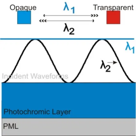
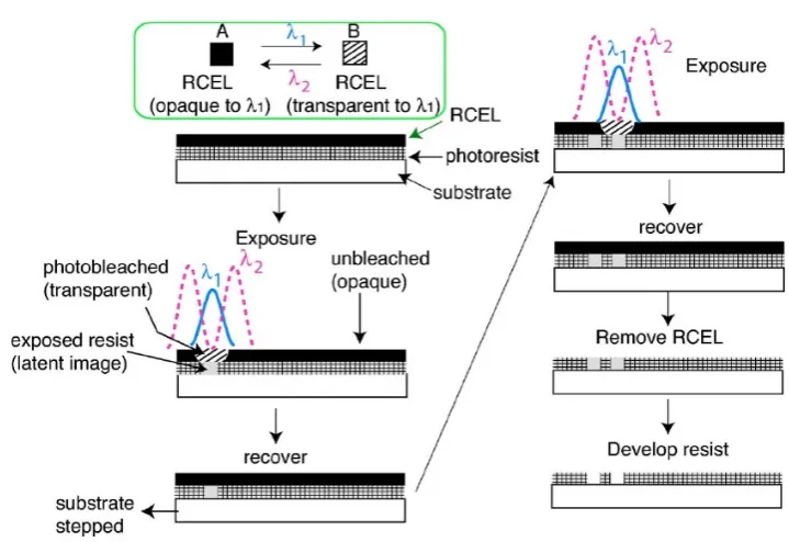
The system of AMOL introduced by papers published in late 2006 and 2007 by Rajesh Menon and Hank Smith at MIT [Menon 2006, Menon 2007] described an optical lithography system using a photochromic azobenzene polymer named PMEA (poly[4-[2-(methacryloyloxy)ethyl] azobenzene]) to create a mask and was broadly related to the microscopy technique of STED [Hell 1994]. The system would involve a thin layer of photoresist spun directly on top of a photoresist. The absorption of this layer could then be changed because of its photochromic nature; a beam at one wavelength, could create a transparent state and a second wavelength, , could create an opaque state. By combining an exposure pattern of and a full pattern could be created consisting of high and low absorbance states, thus an adaptive mask would be formed and because the photochromic material is completely reversible a second pattern may be exposed after the first without additional development steps being required.
sug-gested as a suitable approach. This chapter outlines the development of AMOL, begin-ning with STED microscopy and photochromic layers. It then presents background information regarding surface plasmons and describes the metrics used to clarify imag-ing performance in this thesis.
2.1.1
STIMULATED EMISSIO DEPLETIO MICROSCOPY
Stimulated emission depletion microscopy (STED) is a microscopy technique that makes use of two incident wavelengths and fluorescent molecules that was initially claimed to be able to improve resolution by a factor of 4.5 [Hell 1994], as shown in Fig 2.1. One wavelength is used to excite fluorescence in the molecules, as this is the information of interest; however STED then uses a second wavelength with a ring spatial pattern to suppress fluorescence in the area surrounding the point of interest and hence allow a smaller region to be examined. This technique has demonstrated resolution down to 5.8nm, a factor of 133 improvement on the responsible wavelength [Rittweger 2009], with an example improvement shown in Fig 2.2. Taking this idea and applying it to lithography is an attractive option as Hell has suggested [Hell 2004, Hell 2003]. The major difference between this method and a lithography system based upon it is the interchange of the fluorescent molecules with some other light-dependent medium, such as a photochromic layer.
2.1.2
PHOTOCHROMES
2.1 INTRODUCTION
photochromic materials have shown possible use [Bouas-Laurent 2001, Wilson 1984], including optical data recording [Kawata 2000, Pederson 2000], optical data processing, actinometry and optical switching [Yager 2006, Sasaki 1997]. Photochromism may also have secondary effects alongside the changing colour; the refractive index, the metal ion capture, electron capture, and the shape and size of the polymers and solids have been shown to change, alongside other bulk material properties [Kumar 1989].
There is a large range of molecules which exhibit some form of photochromism, includ-ing spiropyrans, chromenes, fulgides and azobenzenes and the kinetics and chemical pathways of these photochromes vary [Bouas-Laurent 2001]. In this work the focus is placed on a generic photochrome based on an azobenzene. Photochromism in azoben-zene is caused by the incident light causing a change in the cis-trans isomerisation (Fig
Figure 2.1 Principles of a STED fluorescence scanning microscope. An excitation beam and two offset STED beams are focused into the object for excitation and stimulated emission, respectively. The spontaneously emitted light is recorded in a (point) detector. [Hell 1994]
2.4) of the molecule [Yamashita 1962, Barrett 1995]. The photochromism in azobenzene can affect not only the absorbance but also the viscosity, solubility, pH and surface structure among other parameters [Norikane 2004, Kumar 1989] depending on the attached functional groups. The first experimental work in AMOL used an azobenzene (PMEA) photochromic layer as this operated at suitable wavelengths ~400 − 500 and the absorbance change was adequate to allow pattern generation. For a lithography system it is desirable that the masking layer has large differentiation between opaque and transparent regions, this requires the absorbance change of the photochrome to be as large as possible.
Figure 2.3 Changing absorption spectra in a photochromatic material [Andrew 2009]
2.1 INTRODUCTION
2.1.3
ABSORBACE MODULATIO OPTICAL LITHOGRAPHY
– PROGRESS TO DATE
[image:51.595.131.491.434.681.2]Menon and Smith proposed and began basic steps towards making use of the photo-chromic effect in optical lithography [Menon 2006]. The suggested system, shown schematically in Fig 2.5, involved a layer of the photochromic material placed above a layer of photoresist on the substrate. Through careful selection of the pattern and inten-sity of the incident wavelengths, and , a transparent spot may be created in the photochromic layer, allowing to pass through and expose the underlying photoresist. By extension a complex pattern may be formed in the photoresist by a series of serial exposures, shown in Fig 2.5. Thus the AMOL layer may be used as an adaptable mask-ing layer, with the adaptation controlled by optical sources which could be placed in the far-field. A theoretical of improvement in resolution to /13 was proposed [Menon 2006].
A following paper [Menon 2007] detailed an experimental exploration of AMOL (Fig 2.6). Using a Lloyd’s mirror [Born 1999] set-up (Fig 2.7), a standing wave in (532 nm) was created at the surface of the photochromatic layer to provide the
changing intensity ratios between the two wavelengths; a constant intensity of
Figure 2.6 Scanning electron micrographs of lines exposed in negative resist by AMOL system showing average linewidth of 117 nm. [Menon 2007]
2.1 INTRODUCTION
(400 nm) was then also directed onto the layer. Lines of varying widths were created, with a smallest linewidth of 100nm; this limitation was attributed to the thickness of the photoresist. A third paper experimentally demonstrated that multiple exposures could be made using the AMOL system and these could produce spatial frequency multiplication in the exposure pattern; decreasing the period of the grating below the wavelength [Tsai 2007], this verification of the double exposure capabilities demonstrates how AMOL is able to offer improved resolution even though a small duty cycle may be used for a single exposure.
In 2009 a further paper presented the same AMOL system with an alternative photo-chromic material with wider separation of and [Andrew 2009]. Later work by the same group has researched the interaction of AMOL with zone-plate array lithography [Tsai 2008] and the possibilities for microscopy with AMOL [Tsai 2010]. Zone-plate arrays offer a method to create desirable waveforms in both and concurrently using diffractive elements, whilst the opportunity to use AMOL for microscopy uses the confinement provided by an AML to resolve smaller particles.
2.1.4
ADVATAGES OF AMOL
requires operation using the near-field, hence the incorporation of near-field phenomena, such as surface plasmons to improve performance will be required to enhance the AMOL resolution.
2.2
SURFACE PLASMOS
2.2.1
ITRODUCTIO
Many of the intrinsic properties of a metal are caused by the presence of the conduction electrons unbound to the metallic atoms; the interaction of these electrons with electro-magnetic oscillation at optical frequencies has some particularly interesting effects [Zakharian 2007, Pitarke 2005, Maier 2005]. Particular interest is placed on the genera-tion of surface charge oscillagenera-tions on metals with loosely held electrons (Fig 2.8a), known as surface plasmons, as these oscillations are not limited by the wavelength of light, but rather by the electrons’ confinement to the metal surface. Surface plasmons effects have been demonstrated using silver, gold and aluminium as well as other metamaterials, but there is work to find suitable plasmonic metals for different situations [West 2010]. Particular focus has been placed on areas including the combination of surface plasmon effects with circuitry [Ozbay 2006] and surface enhanced raman spectroscopy (SERS) which uses surface plasmons to allow improved measurement [Campion 1998]. The ability to break the diffraction limit as well as bridge the gap between light and circuitry has lead to a large amount of research in different areas of plasmonics.

![Figure 3.2 Actions of a contrast enhancement layer (CEL) showing (a) reduction of edges of exposure profile through CEL placed above resist [Kim 2007]](https://thumb-us.123doks.com/thumbv2/123dok_us/9032124.399641/66.595.110.456.116.418/figure-actions-contrast-enhancement-showing-reduction-exposure-profile.webp)