Optimizing the active region of interband cascade lasers for passive mode-locking
K. Ryczko, J. Misiewicz, S. Höfling, M. Kamp, and G. Sek
Citation: AIP Advances7, 015015 (2017); doi: 10.1063/1.4973937
View online: http://dx.doi.org/10.1063/1.4973937
View Table of Contents: http://aip.scitation.org/toc/adv/7/1
Optimizing the active region of interband cascade lasers
for passive mode-locking
K. Ryczko,1,aJ. Misiewicz,1S. H¨ofling,2,3M. Kamp,2and G. Sęk1
1Laboratory for Optical Spectroscopy of Nanostructures, Department of Experimental
Physics, Faculty of Fundamental Problems of Technology, Wrocław University of Science and Technology, Wybrzeze Wyspia´nskiego 27, 50-370 Wrocław, Poland˙
2Technische Physik, University of W¨urzburg and Wilhelm Conrad R¨ontgen Research Center
for Complex Material Systems, Am Hubland, D97074 W¨urzburg, Germany
3SUPA, School of Physics and Astronomy, University of St. Andrews, North Haugh,
St. Andrews KY16 9SS, United Kingdom
(Received 2 October 2016; accepted 29 December 2016; published online 9 January 2017)
The work proposes possible designs of active regions for a mode-locked interband cascade laser emitting in the mid infrared. For that purpose we investigated the elec-tronic structure properties of respectively modified GaSb-based type II W-shaped quantum wells, including the effect of external bias in order to simultaneously fulfil the requirements for both the absorber as well as the gain sections of a device. The results show that introducing multiple InAs layers in type II InAs/GaInSb quantum wells or introducing a tensely-strained GaAsSb layer into “W-shaped” type II QWs offers significant difference in optical transitions’ oscillator strengths (characteristic lifetimes) of the two oppositely polarized parts of such a laser, being promising for utilization in mode-locked devices. ©2017 Author(s). All article content, except where otherwise noted, is licensed under a Creative Commons Attribution (CC BY) license (http://creativecommons.org/licenses/by/4.0/).[http://dx.doi.org/10.1063/1.4973937]
The mid-infrared range (MIR) is of particular interest for spectroscopic applications as many molecules exhibit characteristic fundamental vibrational/rotational bands in this part of the electro-magnetic spectrum. Laser sources in this spectral region are highly desirable for selective analysis of chemical components that is used in biochemistry, pharmaceutical monitoring, and material sci-ence.1,2One of the recent developments in spectroscopy are frequency combs, which were introduced in the late 1990s and have revolutionized precise measurements of frequency and time. Optical fre-quency combs, generated by mode-locked lasers, can be characterized by broad spectra, consisting of equally spaced and mutually coherent narrow lines. They are creating new opportunities for optical spectroscopy, which is a critical tool for understanding of atomic and molecular structure and has further applications, ranging from semiconductor physics to biology. This is because the frequency of each discrete comb tooth can be referenced to an established frequency standard, thus providing a frequency ruler convenient to probe molecules exhibiting absorption features in a broad spectral region.3 This offers the advantage of spectroscopy without dispersive elements, because the spec-tral position of each mode is encoded in the beat note. In order to further improve the efficiency of direct comb spectroscopy one can use two frequency combs. To perform dual-comb spectroscopy, a sensing comb is transmitted through a sample and then heterodyned against a local oscillator comb, with a repetition rate that differs from the sensing comb rate. Such dual-comb approach exploits the frequency resolution, frequency accuracy, broad bandwidth, and brightness of frequency combs for ultrahigh-resolution and high-sensitivity, and combines many of the strengths of conventional broadband spectroscopy and tunable laser spectroscopy in a single platform.4
Although first demonstrated in the mid-infrared part of the spectrum, dual-comb spectroscopy has been extensively developed in the near-infrared spectral region,5 where frequency combs are
aCorresponding author:[email protected]
015015-2 Ryczkoet al. AIP Advances7, 015015 (2017)
mature sources. It is now also emerging as an appealing tool in MIR high-resolution molecular spectroscopy.6Different approaches have been pursued to obtain mid-infrared frequency combs.7–11 One possibility is the use of mode-locked lasers, which are also of considerable interest for their ability to generate ultra-short light pulses at high repetition rates. Mode locking of lasers has been a subject of intense research because of the complex nonlinear dynamics involving the self-organization of many laser modes.12A multimode laser can be forced to operate in a mode-locked state either passively or actively. Active mode locking is achieved by modulating one control parameter of the laser at a frequency resonant with the separation between longitudinal modes. On the other hand, passive mode locking is commonly achieved by combining two elements, a laser amplifier which provides gain, and a saturable absorber acting as a pulse shortening element. In recent years, remarkable progress in developing passively mode-locked solid state and fiber lasers on GaInAs and GaSb-based semiconductor saturable absorber mirrors (SESAMs) has been achieved, especially near 2µm.13–15 Ultra-short pulse MIR sources have also been developed employing GaSb-based gain mirrors and SESAMs in a semiconductor disk laser cavity.16Additionally, GaSb-based SESAMs exhibit a much faster absorption recovery, with subpicosecond characteristic times.17Also in work,18there has been demonstrated a very compact source of ultra-short optical pulses and MIR frequency combs via the use of fast absorbers for passive mode locking of GaSb-based diode lasers at 2.1µm.
In order to extend the applications of frequency combs to the mid-infrared region of the spectrum one can use a semiconductor-based mid-infrared dual-comb spectrometer in view of its simplic-ity and compactness. So far, in the literature there is an intense discussion about the fundamental mode-locking of quantum cascade lasers (QCLs), which has been a challenge for the last one and a half decades, but has already been demonstrated.19–21Another possible implementation could be a mode-locked interband cascade laser (ICL), of which the first demonstration at 3µm has just been announced.22The ICLs have been well established in the 3-6µm range, and even beyond2,23which could potentially allow for construction of mode-locked devices, which however have additional requirements, including also the respective modification and optimization of the active region to allow for a large enough transition rate difference between the absorber and gain sections.
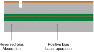
In particular, for a given gain medium, the absorbing medium dynamics should be much faster than the gain medium dynamics, i.e.τa<<τg.24In a semiconductor laser split into the respective two parts, as schematically shown in Figure1, this requirement can be realized by the application of a reverse bias to the absorber region. Therefore, we study the impact of the electric field on the related oscillator strength associated with the fundamental optical transition, which is inversely proportional to lifetime. In this work, we present results of theoretical modelling of the ICLs‘ active region band structure under external electric field, performed in the framework of eight-band k·p theory, in order to investigate the effect of the bias value and direction, i.e. from normal lasing conditions as in the gain section to the reversed bias of the absorber part. We present several solutions for the respectively modified type-II quantum wells (QWs) of an InAs/(In,Ga)(As,Sb)/AlSb materials’ system, which allow obtaining the demanded lifetime (oscillator strength) ratio in the two parts of a mode-locked laser.
A typical W-design AlSb/InAs(1nm)/Ga0.65In0.35Sb(4nm)/InAs(2nm)/AlSb QW structure is
[image:3.594.208.388.617.717.2]illustrated in Fig.2(a) for an electric field equal to 100 kV/cm. General properties of such QWs are discussed in our previous works.25,26 As expected, the maxima of the squared wave function
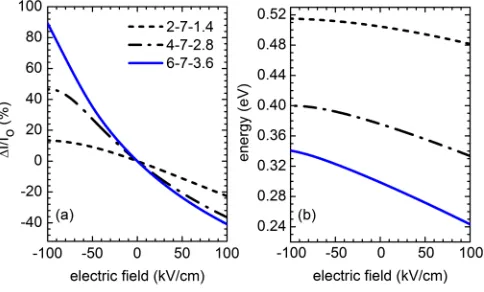
FIG. 2. Confinement potential profile corresponding to the conduction and valence band edges, for a type II W-design QW structure AlSb/InAs(1.0nm)/Ga0.65In0.35Sb(4.0nm)/InAs(2.0nm)/AlSb in external electric field of +100 kV/cm [panel(a)]. In
addition, the probability densities of the fundamental electron and heavy hole states and their energy levels are shown. Part (b) shows the relative change of the squared overlap integral, and part (c) the fundamental transition energy, both in function of electric field. Four different values of the GaIn0.65Sb0.35layer were used as indicated in the legend of Fig.2(b), while keeping
unchanged the thicknesses of the InAs layers.
moduli are in the corresponding layers of InAs and GaInSb for electrons and holes, respectively. Modification of the squared overlap integral is commonly realized via introducing a difference in the thicknesses of the two InAs layers.25,27However, the external electric field changes the assumed or target emission wavelength and affects the overlap integral and spatial carrier separation by intro-ducing an additional asymmetry into the QW confinement potential. In Figure 2(b), we plot the dependence of the fundamental optical transition oscillator strength, expressed by the relative change of the squared overlap integral referred to the zero-field case, i.e.,∆I/I = (I(F)-I(F=0))/I(F=0),as a function of the external electric field (F), whereas in Fig.2(c)the transition energy versus the electric field strength is shown. In the calculations, we use an asymmetric W-design QW structures, in which the Ga0.65In0.35Sb well width changes from 1 nm to 4 nm. Figure2(b)plots the effect of the external
electric field on this relative transition intensity. In particular, in the range of the external electric field of ±100 kV/cm the maximal relative change of the squared overlap integral between the absorber part and the gain section reaches about 30%.
Therefore, for larger differences in the transition oscillator strength (lifetime), a modifica-tion in the active region is necessary, which could lead to stronger sensitivity to the electric field. A possible solution could be the use of structures with a triple type II QW design as e.g. AlSb/InAs/GaInSb/InAs/GaInSb/InAs/AlSb. This type of active region has been used in ICLs emit-ting in the mid infrared in order to enhance the transition oscillator strength28 or to increase the spectral tunability range.29 We choose a system consisting of a triple asymmetric quantum well, because in such a case the wave function is more susceptible to the influence of the electric field. The widths of the layers in the chosen InAs/Ga0.65In0.35Sb/InAs/Ga0.65In0.35Sb/InAs structure are
1.4nm-2.4nm-1.5nm-3.3nm-1.5nm. We define the widths of each layer so to obtain a sufficiently large value of the transition oscillator strength in the case when the structure is placed in an electric field. Figures3(a)and3(b)show the conduction and heavy-hole band edge profiles, the fundamental electron e1 and heavy hole hh1 energy levels and the squared moduli of the corresponding wave functions (expressing the distribution of the probability densities) for such a triple QW, for two elec-tric fields of different sign. Modifying the external elecelec-tric field does not only affect the electronic states for electrons, but it simultaneously influences the holes confined in the two GaInSb layers. This makes the value of the transition oscillator strength a rather strong function of electric field. When the electric field isF= +100 kV/cm, the corresponding probability density distribution of the h1 heavy hole state has a maximum in the thicker GaInSb layer. When the electric field is equal to
[image:4.594.175.419.89.249.2]015015-4 Ryczkoet al. AIP Advances7, 015015 (2017)
FIG. 3. Confinement potential profile corresponding to the conduction and valence band edges, for the modified triple QW design AlSb/InAs(1.4nm)/Ga0.65In0.35Sb(2.4nm)/InAs(1.5nm)/Ga0.65In0.35Sb (3.3nm)/InAs(1.5nm)/AlSb structures, for two
[image:5.594.175.419.90.233.2] [image:5.594.177.419.551.697.2]different values of external electric field: -100kV/cm [panel (a)], and +100 kV/cm [panel(b)]. In addition, probability densities of the fundamental electron and heavy hole states and their energy levels are shown. There is also shown the effect of the external electric field on the relative change of the squared overlap integral [panel (c)] and on the transitions’ energy [panel (d)] for two tripledesign QWs with slightly different InAs layer thicknesses: as for the well in figures (a) and (b) -black dashed line; and for AlSb/InAs(1.4nm)/Ga0.65In0.35Sb(2.4nm)/InAs(1.0nm)/Ga0.65In0.35Sb(3.3nm)/InAs(1.0nm)/AlSb
QW – blue solid line.
the h1 heavy-hole state becomes almost symmetric and the energy level is also altered significantly. The hole has a large and similar probability to be found in both GaInSb layers. Additionally, in this case the e1 electron state penetrates efficiently into the GaInSb barriers. Therefore, the overlap between the conduction and valence band states increases, which is actually driven by the change of electric field. Figure3(c)shows the effect of changing the squared overlap integral via modify-ing the electric field. In particular, it can be observed that increasmodify-ing the external electric field from -100 kV/cm to +100 kV/cm causes a relative change of the squared overlap integral by more than 100%. This result is significantly different from the case of an asymmetric W-design QW. Besides, in order to verify the practical importance, we see that the spectral range of the fundamental tran-sition energy covers a wavelength range from about 3 µm to 6 µm [the effect of the external electric field on the fundamental transition energy is shown in Fig. 3(d)]. Such a triple QW sys-tem can be used even for longer emission wavelengths if the appropriate widths of the layers are selected.
Figure4ashows a similar analysis as in Fig.2(b)and3(c)for the relative change of the squared overlap integral but this time in a type-II W-design of AlSb/InAs/GaAsxSb1-x/InAs/AlSb QW, all
shown in function of the InAs layer thickness for only one value of As content: x = 20%. In our recent
FIG. 4. Effect of the external electric field on the relative change of the squared overlap integral [panel (a)] and the funda-mental transition energy [panel (b)] for three type-II W-design AlSb/InAs/GaAs0.2Sb0.8/InAs/AlSb QW structures; the layer
paper30is has been shown that using the tensile-strained GaAsSb layer in the design of type II QWs, which could potentially be used in the active region of interband cascade lasers, allows gaining in both, lower sensitivity to the inaccuracy of the layer thicknesses during growth and possible enhancement in the transition oscillator strength, while covering the target range in the mid-infrared of at least 3-5µm. Here, we verify the possible application of such a system in mode-locked lasers. As in the case for the AlSb/InAs/Ga0.65In0.35Sb/InAs/AlSb structure, we change the thickness of one of the
two InAs layers in order to engineer the wave functions’ overlap. It turned out that the relative change of the squared overlap integral is strongly sensitive to the external electric field. Changing the electric field from -100 kV/cm to +100 kV/cm causes a change of the squared overlap integral from below -30% to above 120% (calculated with respect to the electric-field-free case), depending also on the thickness of the InAs layers, which can give the relative change even larger than that obtained for a triple QW design.
At the end, this is important to underline that the oscillator strength optimization is only one ele-ment of necessary dynamics engineering on the way towards mode-locked ICLs. In order to achieve mode locking, the carrier lifetime in the absorber segment has to be reduced below the round trip time of the light pulse in the laser resonator (where the latter can only be tailored in a rather limited range by modifying the length of the device). In NIR devices, this is possible by applying a moderate reverse bias to the absorber part. In ICLs in the MIR, transport through the layers is heavily based on minibands that form only in a limited range of the used electrical fields. The full layer structure of an ICL including complicated multilayered injectors has not been taken into account yet. And further, based on our considerations (out of the scope of this paper) this will rather be impossible to use the miniband structure under the reversed bias to extract the carriers efficiently and vertically. Therefore, such solutions as side electrical contacts will need to be developed to exctract the carriers in the plane and to avoid difficulties with the unfavorable miniband structure in the absorber part. An important factor which will need to be considered is also the effectively shorter lifetimes in the gain section of the real device due to influence of non-radiative processes dominated by Auger recombination at room temperature and under high carrier concentrations of an operational device. However, on one hand, one needs to keep in mind that, as shown in Ref.31, that the Auger non-radiative decay rates in similar type-II laser structures appeared to be much lower than it was previously expected. The obtained Auger coefficients also showed no significant dependence on the wavelength in the 3.0–4.2µm window, so in total they play less critical role than in type I MIR lasers. On the other hand, as shown in Ref.22, the kinetics and the losses of the absorber section can be modified independently of the gain one. The Authors used the ion bombardment in order to tailor the losses and to reduce the absorber recovery time. All these indicate on the necessary future developments of the mode-locked ICL devices, including modeling, fabrication as well as experimental characterization of the respective time constants.
Concluding, we have studied the influence of the external electric field on the electronic structure of the type-II QWs of InAs/(In,Ga)(As,Sb)/AlSb materials’ system. We have demonstrated which active region designs can be optimal for a passively mode-locked ICL in a broad range of mid infrared. A significantly enlarged difference in the transition oscillator strength (and related transition rates) between the absorber and gain sections driven by just the external bias can be obtained for triple QWs of AlSb/InAs/GaInSb/InAs/GaInSb/InAs/AlSb or for AlSb/InAs/GaAsSb/InAs/AlSb W-design type II structures. These results can pave the way to the development of a new class of mode-locked devices based on interband cascade concept.
ACKNOWLEDGMENTS
This project has received funding from the European Union’s Horizon 2020 research and innovation programme under grant agreement No 636930 (iCspec).
1C. Y. Wang, T. Herr, P. Del’Haye, A. Schliesser, J. Hofer, R. Holzwarth, T. W. H¨ansch, N. Picqu´e, and T. J. Kippenberg, Nat. Commun.4, 1345 (2013).
2I. Vurgaftman, R. Weih, M. Kamp, J. R. Meyer, C. L. Canedy, C. S. Kim, M. Kim, W. W. Bewley, C. D. Merritt, J. Abell,
and S. H¨ofling,J. Phys. D: Appl. Phys.48, 123001 (2015).
015015-6 Ryczkoet al. AIP Advances7, 015015 (2017)
5I. Coddington, W. C. Swann, and N. R. Newbury,Phys. Rev. Lett.100, 013902 (2008); B. Bernhardt, A. Ozawa, P. Jacquet,
M. Jacquey, Y. Kobayashi, T. Udem, R. Holzwarth, G. Guelachvili, T. W. H¨ansch, and N. Picqu´e,Nat. Photonics4, 55 (2010).
6G. Villares, J. Wolf, D. Kazakov, M. J. S¨uess, A. Hugi, M. Beck, and J. Faist,Appl. Phys. Lett.107, 251104 (2015). 7A. Schliesser, N. Picqu´e, and T. W. H¨ansch,Nat. Photon6, 440–449 (2012).
8E. Sorokin, N. Tolstik, and I. Sorokina,Opt. Lett.38, 299–301 (2013).
9M. A. Solodyankin, E. D. Obraztsova, A. S. Lobach, A. I. Chernov, A. V. Tausenev, V. I. Konov, and E. M. Dianov,Opt. Lett. 33, 1336–1338 (2008).
10P. Maddaloni, P. Malara, G. Gagliardi, and P. De Natale,New J. Phys.8, 262 (2006).
11T. Ideguchi, S. Holzner, B. Bernhardt, G. Guelachvili, N. Picqu´e, and T. W. H¨ansch,Nature502, 355 (2013). 12A. Gordon and B. Fischer,Phys. Rev. Lett.89, 103901 (2002).
13K. Schepler, B. Smith, F. Heine, and G. Huber,Proc. SPIE1864, 186–189 (1993). 14R. C. Sharp, D. E. Spock, N. Pan, and J. Elliot,Opt. Lett.21, 881–883 (1996).
15K. Yang, D. Heinecke, J. Paajaste, C. Kolbl, T. Dekorsy, S. Suomalainen, and M. Guina,Opt. Express21, 4311 (2013). 16A. H¨ark¨onen, J. Paajaste, S. Suomalainen, J.-P. Alanko, C. Grebing, R. Koskinen, G. Steinmeyer, and M. Guina,Opt. Lett.
35, 4090 (2010).
17A. Gluth, Y. Wang, V. Petrov, J. Paajaste, S. Suomalainen, A. H¨ark¨onen, M. Guina, G. Steimeyer, X. Mateos, S. Veronesi,
M. Tonelli, J. Li, J. Guo, and U. Griebner,Opt. Express23, 1361 (2015).
18K. Merghem, R. Teissier, G. Aubin, A. M. Monakhov, A. Ramdane, and A. N. Baranov,Appl. Phys. Lett.107, 111109
(2015).
19G. Villares, A. Hugi, S. Blaser, and J. Faist,Nat. Commun.5, 5192 (2014).
20A. K. W´ojcik, P. Malara, R. Blanchard, T. S. Mansuripur, F. Capasso, and A. Belyanin,Appl. Phys. Lett.103, 231102
(2013).
21S. Barbieri, M. Ravora, P. Gellie, G. Santarelli, C. Manquest, C. Sirtori, S. P. Khanna, E. H. Linfield, and A. Giles Davies, Nat. Photonics5, 306–313 (2011).
22M. Bagheri, C. Frez, I. Vurgaftman, M. Fradet, C. L. Canedy, W. W. Bewley, C. D. Merritt, C. S. Kim, S. Forouhar, and
J. R. Meyer, in29th Annual Conference of the IEEE Photonics Society, 2016.
23R. Q. Yang,Superlattices and Microstructures17, 77 (1995).
24J. B. Khurgin, I. Vurgaftman, and J. R. Meyer,Appl. Phys. Lett.80, 2631 (2002). 25K. Ryczko, G. Se˛k, and J. Misiewicz,J. Appl. Phys.114, 223519 (2013). 26K. Ryczko,Acta Physica PolonicaA126, 1149 (2014).
27K. Ryczko and T. Liszka,Superlattices and Microstructures78, 144 (2015).
28M. Motyka, K. Ryczko, M. Dyksik, G. Se˛k, J. Misiewicz, R. Weih, M. Dallner, S. H¨ofling, and M. Kamp,J. Appl. Phys. 117, 084312 (2015).
29Y. Jiang, L. Li, Z. Tian, H. Ye, L. Zhao, R. Q. Yang, T. D. Mishima, M. B. Santos, M. B. Johnson, and K. Mansour,J. Appl. Phys.115, 113101 (2014).
30K. Ryczko, G. Se˛k, and J. Misiewicz,Applied Physics Express8, 121201 (2015).
31I. Vurgaftman, C. L. Canedy, C. S. Kim, M. Kim, W. W. Bewley, J. R. Lindle, J. Abell, and J. R. Meyer,New J. Physics11,
![FIG. 2. Confinement potential profile corresponding to the conduction and valence band edges, for a type II W-design QWstructure AlSb/InAs(1.0nm)/Ga0.65In0.35Sb(4.0nm)/InAs(2.0nm)/AlSb in external electric field of +100 kV/cm [panel(a)]](https://thumb-us.123doks.com/thumbv2/123dok_us/8983632.394886/4.594.175.419.89.249/connement-potential-prole-corresponding-conduction-qwstructure-external-electric.webp)