ISSN Online: 2153-1188 ISSN Print: 2153-117X
New Method of Thermal Energy—To Electrical
Energy Conversion in Vacuum Devices with the
Metal—Dielectric Nanofilm Electron Sources
V. E. Ptitsin
Institute for Analytical Instrumentation of the Russian Academy of Sciences, Saint-Petersburg, Russia
Abstract
New method of thermal energy—to electrical energy conversion in vacuum devices with the metal (W)—dielectric nanofilm (ZrO2) electron source is offered and studied. According to estimates and results of modeling, the energy effectiveness (χ) of the proposed method may exceed χ for the known thermionic energy conversion method to 2 - 3 orders of magnitude.
Keywords
Energy Conversion, Thermionic Emission, Metal-Dielectric Nanofilm, Nanostructures, Abnormal Thermal Field Electron Emission
1. Introduction
Achievements of last decades in the area of micro-and nanotechnology pro-moted revival of scientific interest to a problem of direct transformation of thermal energy to electrical energy. As a result of development of nanotechnol-ogy methods, researchers had new possibilities for use in the workings out of the fundamental physical phenomena which remained earlier not claimed. In par-ticular, reproduced formations of quasi 1D and 2D nanostructures (NS) have al-lowed to start working out on the thermionic energy conversion devices with the single-crystal n-type diamond electron sources (cathodes) [1].
The main aim of this work is to, on the basis of new ideas about the mechan-ism of the abnormal thermal field emission from the metal-dielectric nanofilm structures [2], propose and justify the opportunity to design an original and more energy effective method compared to known thermionic energy conver-sion (TEC) method [3].
How to cite this paper: Ptitsin, V.E. (2018) New Method of Thermal Energy—To Elec-trical Energy Conversion in Vacuum De-vices with the Metal—Dielectric Nanofilm Electron Sources. Materials Sciences and Applications, 9, 1073-1082.
https://doi.org/10.4236/msa.2018.913078
Received: November 26, 2018 Accepted: December 23, 2018 Published: December 26, 2018
Copyright © 2018 by author and Scientific Research Publishing Inc. This work is licensed under the Creative Commons Attribution International License (CC BY 4.0).
http://creativecommons.org/licenses/by/4.0/
Open Access
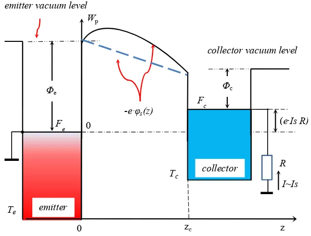
It should be noted that converting thermal energy to electrical power in the themionic converter (TC) is achieved by electron emission and passing of an electron current from the emitter to the collector in the electrostatic field pro-duced by a contact potential difference between electrodes (emitter and collec-tor). Figure 1 shows the energy diagram that makes it easy to understand (or remember) the known principle of TC action.
At present the TEC method is developed in a sufficient measure [3]. This me-thod permits implementation of the energy conversion (EC) process with the ef-ficiency η ~ 20% and the energy effectiveness (χ)
(
)
1
S c S e c
J V eJ
χ
= ⋅ ≡ Φ − Φ ,where JS—saturation thermionic current density for the emitter substance; Φe, Φc—work function (in eV) of the emitter and collector TC, respectively, about ~10 W/cm2.
As is known [3], TEC method has two major drawbacks.
[image:2.595.217.525.425.659.2]First or technical—technological disadvantage is the need to have heated to high temperatures (~2000 K) TC electrodes at very small distances. Physically small size of the vacuum gap is determined by the strong influence of the ther-mionic electrons space charge (SC) field on the TC conductivity [3]. The second fundamental flaw of this method is that the saturation current density of the TC effective emitters is only about ~10 A/cm2. An analysis of literature data [4] should be that, to date, the potential for further development of the TEC method is largely exhausted and the substantial improvement in its technical and operational
Figure 1. Energy diagram showing the principle of the TC operation. Here Φe, Φc, Te, Tc—work function and temperature of the emitter and collector TC, respectively. Is—saturation current at the emitter working temperature; zc (zc < 100 µm) is the optimal value of the gap between TC electrodes. Direct line (blue) corresponds to the potential distribution, if not to take into account the effect of SC field.
-e∙φs(z)
Wp
0
emitter vacuum level
z 0
Φe
zc
(e∙IsR)
emitter
Fc Φc
Fe
collector vacuum level
collector
I~Is R
Te
Tc
specifications may only as a result of significant changes in the physical basis of this method. At first glance, to correct the above deficiencies of the TEC method possible to try to create a new vacuum device for energy conversion, in which thermionic cathode would be replaced by a thermal field electron emitter with high emission current density (up to ~108 A/cm2 [5]). In addition, as shown in a work [6] the influence of space charge (SC) field on the thermal field emission (TFE) process very low and, therefore, to effectively transfer the emitted electron flow to the device collector is no longer required to bring the electrodes to a very small value vacuum gap (<100 µm).
2. Physical Simulation of the Vacuum Thermal-to-Electrical
Energy Converter Prototype with High Energy Effectiveness
For creation of the vacuum energy conversion device prototype with high energy effectiveness, it is clear that electront source of the created converter should have high emission capacity. At the beginning of our research, we assumed that for this purpose can be used high current density TFE electron source. It is essential that this electron source and electron-optical system (EOS) of the new energy conversion device prototype must satisfies a number of obvious physical condi-tions.1) Emitting surface of the device electron source (cathode) should have high curvature. As the cathode can be used a single microtip or also an ordered en-sembles of the microtips, quantum dots, and carbon nanotubes.
2) In such device must be running condition for physical “separation” of the two interrelated processes—electron emission and electron transport processes. To realize this condition was proposed to introduce in the traditional thermionic converter diode system additional extracting electrode that allow create on the structured cathode surface necessary high electric field (up to ~107 V/cm). Addi-tional extracting electrode allows create necessary conditions for high intensity e-flux emission. For the subsequent transport of the e-flux from the cathode to the collector surface with a potential that approximately equal to contact poten-tial difference (between the cathode and the convertor collector) it was suggested to use the known magnetic isolation method. Magnetic isolation allows prevent direct capture (or deposition) of an electrons by the extracting electrode under electrical field acting.
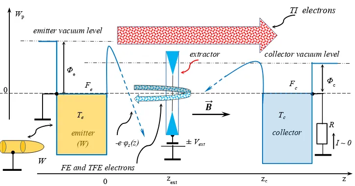
Phenomenological scheme of the emission and electron transport processes in the thermal-to-electrical energy converter prototype with nanostructured surface of TFE electron source is shown on Figure 2. From Figure 2 of the phenome-nological scheme, of course, impossible to understand whether the proposed approach physically reasonable. In order to ascertain the validity of the proposed schemes for energy conversion devices, you must first find out whether emitted an electron to reach the surface collector in the specified physical conditions. In other words, be sure that after extraction the electron moving in the EOS con-verter potential field, the energy conservation law will not be disturbed.
Figure 2. Phenomenological scheme of the emission and electron transport processes in the thermal-to-electrical energy converter prototype with nanostructured surface of the electron source; Vext—extracting voltage; B
—induction of a uniform magnetic field.
For ease of analysis, it will assume that the cathode is a single metal (W) tip, that depending on the values of the Te and Vext can play the role of either ther-mionic cathode or thermal field emitter (cathode) as well as at low temperature Tethe metal tip can be considered as a field emitter (cathode). Let also Φe> Φc.
In addition, we will consider the initial stage of each of the possible emission processes. That is, immediately after the inclusion of the extracting electrostatic field and the magnetic field. In this initial phase Fermi levels of the cathode and collector will still one and the same value on the energy scale. Taking into ac-count the comments made above, Figure 2 can be represented in a more infor-mative (space-energy) form (see Figure 3).
For clarity, we will assume that the field strength at the W emitter surface is sufficient for field electron emission and the emitter temperature can vary widely from 300 K to 2500 K.
In order to qualitatively to provide processes that must occur in the proposed version of the EOS converter will be based on three known fundamental physical principles.
1) In contact two or more solid bodies the Fermi levels of these bodies take the same value.
2) When charge move in a potential force field the total energy of the charge remains constant.
3) In a result of an electron tunneling from the metal in vacuum it total energy does not change.
At relatively low temperatures (<500 K) in this conversion device the domi-nant emission process is the process of field emission (FE). In these circums-tances, electron emitted in vacuum by the tunnel mechanism, after acceleration will be reflected from the barrier: vacuum-collector. In these conditions, reach
Figure 3. Phenomenological functional scheme of the different electron emission and transport processes in the thermal-to-electrical energy converter prototype with the single metal (W) tip as an electron source; abbreviations: TI—thermionic, FE—field emission, TFE—thermal field emis-sion.
the collector surface can only thermionic emission (TI) electrons that emitted in vacuum over barrier: metal-vacuum, as well as the TFE electrons from the “tail” of the energy distribution function of an electrons in the metal (W). In addition, the emergence of TI current in the converter closed circuit will lead to “rise” up collector potential box in energies scale that blocks the opportunity to partici-pate of the TFE electrons in forming the full TC current. At high temperatures (2000 K < Te< 2500 K) considered here the original EOS will function only as a converter of the thermal energy into electrical energy as a result of the TI process.
Thus, according to the qualitative analysis, the shift from the traditional EOS of the TI converter on proposed here EOS with three electrodes, gives no reason to believe that such a move could allow any significantly improve χ of the new type converter due to the contribution in energy conversion process intensive flows of FE and TFE electrons.
However, it is important to note that the offered EOS allows significantly in-crease the gap between the emitter and collector of electrons, and make it quite acceptable (more than ~(1 - 5) cm) for prolonged use of the TC at high temper-atures.
Another very important conclusion that follows from the previous review is that in order to improve the energy efficiency of thermal energy converter in electric energy it is necessary that electron source converter emitted in vacuum high intensity electron flux with full initial electron energy E, which would sub-stantially exceed the height barrier: vacuum-collector (Figure 3). It is clear that such a “hot” electrons flow without dissipation at this barrier can freely inject into collector. In the next section it is shown that the required emission proper-ties have some metal-nanofilm structures (W/ZrO2, Mo/ZrO2) [2].
Wp
0
emitter vacuum level
z 0
± Vext
R
zc
I ~ 0 emitter
(W)
Fc Fe
collector vacuum level
zext
collector
-e∙φs(z)
Te Tc
extractor
Φe
Φc
𝑩
��⃗
FE and TFE electrons
TI electrons
W
3. Abnormal Thermal Field Emission Electron Sources for
Thermal to Electrical Energy Converters
More than ten years ago the author of this work, in the research of high-current electron sources has been found that W/ZrO2 metal-nanofilm (MNF) structure at under certain conditions has unique emission properties [2]. It has been re-vealed that in relatively low macroscopic (external) electrical fields (below ~500 V/μm) and at the material temperatures within 1950 K to 2150 K the MNF shows an abnormally high normalized brightness (up to ~106 A/(cm2 sr V)) and high stability of field emission properties. The revealed phenomenon of a sharp rise in emissive ability of the W/ZrO2 in a certain range of ZrO2 layer thicknesses and substance temperatures was called “Abnormal Thermal Field Emission” (ATFE). A phenomenological model of the physical mechanism of the ATFE from planar MNF surfaces was developed. The opportunity of use of found out and investigate unique thermal field emission properties W/ZrO2 structures in high current density electron sources and in energy conversion devices was of-fered and discussed in [7].
The phenomenological model of the ATFE phenomenon is constructed on the basis of generalization of the data obtained in the present study of field emission properties of low-dimensional nanostructures [2].
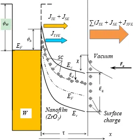
These data, in particular, show that specific features (or anomalies) of the process of field emission from the surface of such NS are substantially defined by physicochemical and structural properties of the superficial nanofilm which usually represents nanostructure consisting of metal or semi-conductor sub-strates and a thin dielectric layer. The thin dielectric nanofilm on the surface of the substrate is created is artificially by means of modern technological methods or is formed naturally as a result of oxidation of the substrate surface. Taking into account these remarks, to construction the model of ATFE from the surfac-es of low-dimensional nanostructursurfac-es in a real vacuum diode was modeled by a 2D structure: metal—a thin dielectric nanofilm placed into vacuum under a homogeneous electrostatic field of strength Fe (Figure 4).
The ATFE model was based on the following assumptions [2].
1) Electron injection from metal to dielectric through the metal-dielectric in-terface, can involve both the thermal field emission and thermionic mechanisms; the metal-dielectric junction is locking for metal electrons;
2) Electric field on the metal-dielectric interface is a superposition: of external field(Fe), positive space charge (SC) field formed as a result of ionization of the localized states in the band gap of the dielectric film and also of SC field of elec-trons injected into the dielectric conduction band;
3) Ionization of the localized states in the band gap of the dielectric film may occur both by thermal field mechanism and, generally speaking, under action of the electromagnetic radiation absorbed by the film, including thermal radiation of the emitter substance;
4) At small thicknesses of a dielectric nanofilm (about the free path length of
Figure 4.Two barrier energy band diagram for ATFE phenomenon theoretical modeling.
low-energy electrons in relation to the process of electron-phonon interaction) electron transport in the film is occurs mainly by the quasi-ballistic mechanism;
The results of the analytical modeling of ATFE were in good agreement with the experimental data [8]. In particular, it was shown that the total ATFE cur-rent density can reach values ~108 A/cm2. The ATFE process and, consequently, emission current at the fixed MNF temperature and extracting voltage Vext val-ues is characterized by high stability [9].
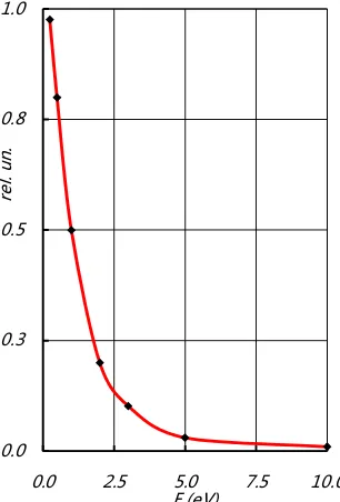
With regard to the subject of this work is also important to note the results of measurements of the energies distribution emitted electrons in ATFE process (Figure 5). As you can see from the electron energy distribution curve in the flow of the ATFE the relatively large number of electrons (~5% - 10%) have a primary energy more ~4 eV. Physically, this means that if you use the ATFE emitter in the energy converter prototype (Figure 3) that ~(0.05 - 0.10) ATFE flow will inject in the collector over the potential barier: vacuum-collector. Ac-cording to estimates and results of numerical modeling [7], the power density of the “hot electrons” on the collector surface can reach high values, the order of ~(103 - 104) W/cm2 or higher.
4. Conclusions
Research shows that the energy effectiveness of the traditional TI energy conver-sion method can be significantly (to the 2 - 3 orders of magnitude) increased through use in the new type energy converter with electron source based on the
E
FW
Vacuum
x
Nanofilm
(ZrO
2)
E
vE
FEg
Surface
charge
SC
Fe
J
TE+ J
SEJ
TFEτ
E
cφ
bEd
χ
∑(J
TE+ J
SE+ J
TFE)
φ
WFigure 5. Typical curve for distribution of the ATFE electrons on the full initial energies in vacuum.
special MNF structures that are efficient emitters of a high current density elec-tron flux in the necessity for initiating ATFE process physical conditions.
To create the necessary physical conditions, the EOS of a new type energy converter must contain (in addition to the emitter and collector) special third electrode-extractor. Additionally, the EOS should include the source of a uni-form magnetic field that required for magnetic isolation of the emitted electron flux.
The results can be easily consolidated at a large electron emitting surfaces on which by the modern techniques of nanotechnology can be grown ordered en-sembles of the quantum dots or nanowhiskers each of which acts as point elec-tron emitter in the physical conditions needed for the ATFE process excitation.
ATFE properties: super high emission ability and stability of process, rather low level of Fe and also high density of emission current (up to 108 A/cm2 and more) can be used in different areas of micro- and nanoelectronics, including high power electronics to produce high-intensity stationary electron sources and also in the area of energy transformation for development of effective systems for direct small-scale energy conversion devices requires portable electrical power to drive electronic components as well as a compact cooling system to maintain the temperature of the primary electronic components within a narrow range at or below ambient. Similar needs for efficient, small-scale cooling and/or power generation will persist for many future engineering applications.
The ATFE phenomenon relates generally to energy conversion devices, and more particularly, this phenomenon pertains to the use of W/ZrO2 electron emitters in thermodynamic energy conversion devices. The need for efficient, reliable, and cost-effective small-scale energy conversion devices is increasing
0.0 0.3 0.5 0.8 1.0
0.0 2.5 5.0 7.5 10.0
re
l. un.
E (eV)
due to the downsizing of commercial and military products that require either electrical power or compact cooling.
W/ZrO2NS does not seem to be unique in its physicochemical and structural properties. To form new MNF-effective ATFE electron sources (based both on 1D or 2D structures and ordered ensembles NS) having a priori given emission properties (in particular, excitations of the ATFE process at T = 300 K) addi-tional special researches using the latest methods for modeling of processes of layer-by-layer epitaxial growth of thin dielectric films on the surface of transi-tion metals (and also of n-type semiconductors) and methods of “zone engi-neering” are necessary [1] [10].
Acknowledgements
This research was supported of FASO Russia (state task, Project No. AAAA-A16-116041110123-5).
Conflicts of Interest
The authors declare no conflicts of interest regarding the publication of this pa-per.
References
[1] Koeck, F.A.M. and Nemanich, R.J. (2017) Advances in Thermionic Energy Conver-sion through Single-Crystal n-Type Diamond. Frontiers in Mechanical Engineering, 3. https://doi.org/10.3389/fmech.2017.00019
[2] Ptitsin, V.E. (2011) Phenomenological Model of an Abnormal Thermal Field Elec-tron Emission from the 2D Nanoheterostructured Surfaces. Journal of Physics: Conference Series, 291, 012019. https://doi.org/10.1088/1742-6596/291/1/012019 [3] Hatsopoulos, G.N. and Gyftopoulos, E.P. (1973) Thermionic Energy Conversion,
Vol. I, (1973), Vol. II, (1979). MIT Press, Cambridge, MA.
[4] Ptitsin, V.E. (2013) Current State and Prospects of the Energy Conversion Ther-mionic Method Development. Scientific Instruments, 23, 25-39.
[5] Ptitsin, V.E. (2000) Non-Stationary Thermal Field Emission. In: Hawkes, P.W., Ed. Advances in Imaging and Electron Physics, Academic Press, 112, 165.
[6] Ptitsin, V.E., Komyak, N.I. and Kol’tsov, S.N. (1998) On The Effect of the Space-Charge Field of Emitted Electrons on Thermal Field Emission. Doklady Physics, 43, 678-681.
[7] Ptitsin, V. (2014) New Approach to Thermal-to-Electrical Energy Conversion Problem on the Bases of the Thermal Field Electron Emission Phenomenon. In: 10th International Vacuum Electron Sources Conference (IVESC) & Second Inter-national Conference on Emission Electronics (ICEE), 230-231. Published: 1 June 2014 by Institute of Electrical and Electronics Engineers (IEEE) in 2nd International Conference on Emission Electronics (ICEE), 1-3.
https://doi.org/10.1109/Emission.2014.6893976
[8] Ptitsin, V.E. (2007) Anomalous Thermal Field Emission, Technical Physics. The Russian Journal of Applied Physics, 52, 504-509.
[9] Ptitsin, V.E. (2010) New High Brightness and Stability Point Electron Source.
ceedings of the 8th International Vacuum Electron Sources Conference and Nano-carbon, IVESC 2010 and NANOcarbon, 180-181.
[10] Robert, P. and Livio, B. (2017) Nanoelectronics: Materials, Devices, Applications, 2 Volumes, Wiley-VCH.