System-on-Chip Design Using High-Level Synthesis Tools
Erdal Oruklu1*, Richard Hanley1, Semih Aslan2, Christophe Desmouliers1,
Fernando M. Vallina3, Jafar Saniie1
1Department of Electrical and Computer Engineering, Illinois Institute of Technology, Chicago, USA 2Ingram School of Engineering, Texas State University, San Marcos, USA
3Xilinx Inc., San Jose, USA Email: *[email protected]
Received August 13, 2011; revised November 20, 2011; accepted November 30, 2011
ABSTRACT
This paper addresses the challenges of System-on-Chip designs using High-Level Synthesis (HLS). HLS tools convert algorithms designed in C into hardware modules. This approach is a practical choice for developing complex applica-tions. Nevertheless, certain hardware considerations are required when writing C applications for HLS tools. Hence, in order to demonstrate the fundamental hardware design concepts, a case study is presented. Fast Fourier Transform (FFT) implementation in ANSI C is examined in order to explore the important design issues such as concurrency, data recur-rences and memory accesses that need to be resolved before generating the hardware using HLS tools. There are addi-tional language constraints that need to be addressed including use of pointers, recursion and floating point types.
Keywords: System Level Design; High Level Synthesis; Field Programmable Gate Arrays; Fourier Transform
1. Introduction
In the past decade, there has been a substantial increase in the level of hardware abstraction that High-Level Synthesis (HLS) [1-5] tools offer, which has made de-signing a complete System-on-Chip (SoC) much more practical. By designing at the system level, it has become possible for hardware engineers to avoid gate-level se-mantics. HLS tools work by taking applications written in a subset of ANSI C, and translating it into a Register Transfer Level (RTL) module for Application-Specific Integrated Circuit (ASIC) or Field Programmable Gate Arrays (FPGAs) chip design. The design workflow re-quires knowledge of both software to write C applica-tions and hardware to parallelize tasks, resolve timing and memory management issues. There has been signifi-cant previous work that discusses how to teach RTL con- cepts to students and design simple applications for SoCs [6,7]. Nevertheless, the learning curve for software engi-neers is relatively high since they need to use Hardware Descriptive Languages (HDL) such as Verilog and VHDL. By using HLS tools, software engineers can use their pro- gramming skills along with hardware knowledge to create complex embedded hardware/software co-design systems.
To demonstrate the critical hardware and software de-sign issues, a Fast Fourier Transform (FFT) [8] case study is used as a guideline. In order to generate hard-ware modules satisfying predefined constraints such as
through-put and area, different modifications of the code required by HLS tools are presented step by step.
Section 2 of this paper provides a brief background of HLS tools, and the current pedagogical techniques. Sec- tion 3 presents an introduction of the FFT algorithm along with a software implementation. This software based FFT is then deconstructed in Section 4, where a fully synthesizable product is created. Section 5 analyzes the different results that can be produced depending on the constraints selected by the user such as speed, area, throughput, and targeted system.
For this paper, all designs are targeted for the Xilinx Virtex-5 FPGA platform [9] using the HLS tool called PICO, provided by Synfora Inc [10] (currently known as Synphony C Compiler by Synopsys [11]). However, the different code modifications presented in this paper are applicable to other HLS tools such as AutoESL [12] which targets primarily Xilinx FPGAs with architecture aware synthesis and Catapult C [13] which provides full- chip high-level synthesis for both ASIC and FPGA de-vices and automatic RTL verification.
2. High Level Synthesis Tools
This section outlines the important concepts that software developers need to know before entering the field of HLS. There is a special emphasis on how these concepts differ from the contemporary software environment familiar to the software engineers. Design of SoCs has historically
been accomplished using Hardware Descriptive Lan-guages such as VHDL or Verilog. Each expression in HDL represents a group of gates that operate in parallel, as opposed to machine instructions executed sequentially. This concept of instruction level parallelism is one of the first major hurdles when introducing hardware concepts.
Once an RTL module is designed, it can be compiled and simulated. The simulation is done by creating a se-ries of pdefined inputs, known as a testbench, and re-cording the outputs. If a module passes the simulation then a low level implementation can be created. This low level implementation then enters the verification process to ensure that all timing dependencies are met. In prac-tice, simulating and verifying an implementation can take 50% - 60% of the development time, increasing the time- to-market (TTM) [14]. By automating the simulation and verification process, it is possible to greatly reduce the development time.
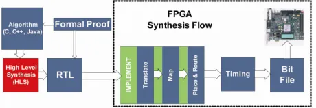
Integration of HLS tools into the FPGA or ASIC de-sign flow, as shown in Figure 1, allows software
[image:2.595.315.535.424.721.2]design-ers to build hardware modules and speed up the TTM significantly. During the generation process of an RTL module from a software implementation, simulation and verification are done automatically by using a formal proof provided during the initial steps. Subsequently, by using synthesis tools, the RTL module is implemented and timing verification is done. An independent evalua-tion of HLS tools for Xilinx FPGAs has been done by Berkeley Design Technology [15]. It shows that using HLS tools with FPGAs can improve the performances of an application by an order of magnitude compared to DSPs. Moreover, this study shows that for a given appli-cation, HSL tools will achieve similar results compared to hand-written HDL code with a shorter development time. HLS software based approach for simulation and veri-fication is made possible by using SystemC, a language developed by Synopsys, University of California Irvine, Frontier Design and IMEC. SystemC is an extension of C++ that provides additional libraries to design an em-bedded system. The first version was released in 1999 and in 2005 it became IEEE standardized SystemC [16, 17] as the IEEE-1666-2005. These additional libraries make it possible to specify the hardware and software components in an embedded system using one unified paradigm and to generate testbenches.
Figure 1. FPGA high level synthesis block diagram.
Focusing further on HLS, the design flow is shown in
Figure 2. Each module of a system is implemented using
high level languages such as C, C++, Java, or Matlab [2,18], which can then be tested automatically with test-benches provided by the user. After verification of the complete system, the user can specify in the HLS tool which modules will be converted into hardware accel-erators in order to speed up the application. This is one of the core elements of hardware/software co-design that software developers need to understand. There are in-herent restrictions in the HDLs that are mirrored in the HLS tool. Therefore, the emphasis for teaching HDL to software developers is on its constraints and how it af-fects the HLS tools.
After generation of the hardware modules along with testbenches, the system is verified and can be imple-mented using synthesis tools.
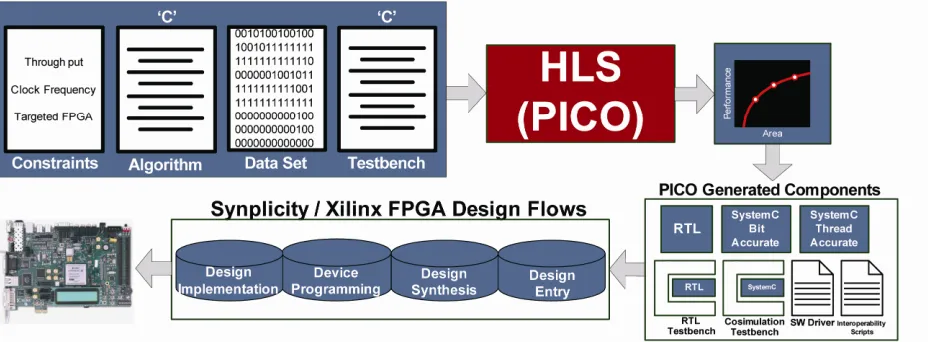
This paper, as mentioned earlier, focuses on designing a Fast Fourier Transform. The concept of HLS is pre-sented by using PICO (Program-In Chip-Out) Extreme from Synfora [10,19,20] to generate the RTL code of an FFT. To be specific, PICO takes a C-based description of an algorithm and generates: performance-driven device- dependent synthesizable RTL code, testbench files, ap-plication drivers, simulation scripts as well as SystemC based Transaction Level Models (TLM) [3,17,18,21]. PICO design flow is shown in Figure 3. With integration
[image:2.595.58.288.640.719.2]Figure 3. HLS (PICO) based design flow for hardware implementation.
of the PICO design tools to their FPGA flow, designers can create complex hardware [20] sub-systems from se-quential untimed C algorithms. It allows designers to explore programmability, performance, power, area and clock frequency. This is achieved by providing a com-prehensive and robust verification and validation envi-ronment. PICO is designed to explore different type of parallelism and will choose the optimal one transparently. Results in terms of throughput and area are given along with detailed reports that will help the user for code op-timization. When the synthesized performances are sat-isfactory, RTL code is generated and can be implemented in the targeted platform. Because the testing is done in C, the verification time of the RTL module can be signifi-cantly reduced [20].
3. Fast Fourier Transform
In most cases, the first step when using an HLS tool is to create a reference implementation, which is used to ver-ify the synthesized product. The reference code itself can be compiled using any C compiler, and is purely soft-ware based. This means that no new concepts have to be taught, making the reference implementation a logical starting point when using HLS.
When creating the reference code for FFT, there are few issues that need to be addressed when using HLS tools. The first issue is that arithmetic operations such as division can significantly decrease the performance of the design, and therefore should be avoided whenever possible. Nevertheless, division by a power of two is considered as a bit shift operation and hence can be used at no cost. The second issue, and more fundamental issue, is that pointers and recursion are not supported by the current HLS tools due to the fact that those concepts are purely software and can’t be applied to hardware designs. Finally, HLS tools may not have the capability to synthe-size software functions such as cosine and sine. As a
re-sult of these constraints, the reference code included in this section does not use divisions, is completely iterative, and has not pointer variables. However, before going into the details of the implementation, the mathematical back- ground of the FFT is presented.
3.1. FFT Algorithm
The Fourier transform takes a signal x in time t and trans- forms it into a function X in frequency ω:
2π
( ) ( )* j td
X x t e t
(1)The transform can be computed using a Discrete Fou-rier Transform (DFT).
1 2π
0
n
N j k
N
k n
n
X x e
(2)0, , 1
k N .
where
The direct realization of DFT algorithm requires O(N2) computational time. To make this computation faster, an entire class of Fast Fourier Transforms (FFT) were de-veloped [8]. However, in this paper a radix-2 FFT deci-mated in time is implemented. This algorithm divides the original DFT into two DFTs with half the length (i.e.
decimation). The first step in decimation is shown below:
1 2π 1 2π
2 2 2 2
2 2 1
0 0
N N
j j
m k m k
N
k m m
m m
X x e x e
N 1 (3)Then the algorithm is recursively applied to each term until each DFT’s length is 1. This recursive deconstruc-tion of the DFT makes the computadeconstruc-tional time of
O(Nlog(N)) [8].
3.2. Software Implementation of the FFT
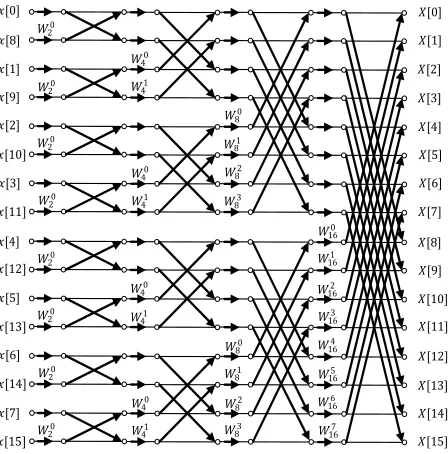
20 20 20 20 20 20 20 20 [0] [8] [1] [9] [2] [10] [3] [11] [4] [12] [5] [13] [6] [14] [7] [15] 40 40 40 40 41 41 41 41 80 81 82 83 80 81 82 83 160 161 162 163 164 165 166 167 [0] [1] [2] [3] [4] [5] [6] [7] [8] [9] [10] [11] [12] [13] [14] [15] Figure 4. 16-point radix-2 FFT.
inputted into the FFT in a bit reversed order and then goes through log2(N) passes, where each pass has N/2 “butterfly” operations. These butterfly operations are defined as:
k N
W f
g G
O
2π
k jk
N
W e N (called the Twiddle factor)
k N k N
F f W g
G f W g
(4)
The butterfly operation requires complex number arithmetic additions and multiplications. Because of the programming constraints placed on the reference code, most complex number libraries are not useable. Hence, this reference code uses its own complex number repre- sentation shown below:
{ ; ; } _ ; typedef struct float x float y s complex
Moreover, in order to perform the butterfly operation, the k
N
W terms need to be calculated. Since we assume that HLS library does not support cosine and sine func-tions, the twiddle factors are pre-computed and stored in a table using the code below:
# " . "
# .
# 2 ( )6.28318530717958647692528676655901
_ _ [ / 2];
_ ( )
{
0.0; 2 / ;
_ , _ ;
; ( include fft h include math h define pi double extern s complex fix float N void table setup void
double a double e pi N
float cos val sin val int i
for
0; / 2; ){
_ cos( );
_ sin( );
_ [ ]. _ ;
_ [ ]. _ ;
; } }
i i N i
cos val a
sin val a
fix float i x cos val fix float i y sin val a a e
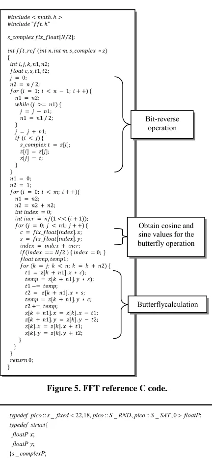
The particular implementation chosen for this refer-ence FFT was provided by [22]. The exact code used is shown in Figure 5. N represents the length of the FFT
and must be a power of 2. Before using the function
fft_ref, the function table_setup must be executed in or-der to compute the twiddle factors and store them in the array fix_float. The FFT of an input z can then be exe-cuted. The first phase is the bit-reverse operation where the input data are rearranged as show in Figure 4. Then,
for each passes, the butterfly operations are performed until the FFT is completed. In the next section this code will be made fully synthesizable by applying four modi-fications to it.
4. Code Modification for HLS
The objective of this section is to generate the hardware of a FFT block based on the reference C code using HLS tools. Multiple modifications are needed in order to ge- nerate an optimal hardware in term of resource usage and throughput. As an example, we generate an 8-bit 1024- point radix-2 FFT. The output is on 18 bits and will beavailable in natural order. The size of the data width inside the FFT has been chosen so that the HLS FFT gives the same results as the Xilinx FFT core [23].
[image:4.595.61.285.88.315.2]# < ℎ. ℎ > # " . ℎ"
_ _ [ /2]; _ ( , , _ ∗ ) {
, , , 1, 2; , , 1, 2; = 0; 2 = / 2;
( = 1; < − 1; + +) { 1 = 2;
ℎ ( >= 1) { = − 1; 1 = 1 / 2; }
= + 1; ( < ) { _ = [ ]; [ ] = [ ]; [ ] = ; } } 1 = 0; 2 = 1;
( = 0; < ; + +){ 1 = 2;
2 = 2 + 2; = 0;
= /(1 << ( + 1)); ( = 0; < 1; + +) { = _ [ ]. ; = _ [ ]. ; = + ; ( == /2 ) { = 0; } , 1;
( = ; < ; = + 2) { 1 = [ + 1]. ∗ ); = [ + 1]. ∗ ); 1 −= ;
2 = [ + 1]. ∗ ; = [ + 1]. ∗ ; 2 += ;
[ + 1]. = [ ]. − 1; [ + 1]. = [ ]. − 2; [ ]. = [ ]. + 1; [ ]. = [ ]. + 2; }
} } 0; }
Bit-reverse operation
Obtain cosine and sine values for the butterfly operation
[image:5.595.63.279.76.548.2]Butterflycalculation
Figure 5. FFT reference C code.
:: _ 22,18, :: _ , :: _ ,0 ;
{ ; ;
} _ ;
typedef pico s fixed pico S RND pico S SAT floatP typedef struct
floatP x floatP y s complexP
FFT is computed using 22-bit data width with 18 bits for the integer part and 4 bits for the fractional part. Rounding and saturation configuration is used. The effect of the number of bits allocated to the fractional part on the precision and resource usage of the FFT HLS is pre-sented in Section V. The twiddle factors are pre-calcu- lated with a precision of 16 bits and stored in an array eliminating the need of trigonometric functions.
4.2. Input Array to Stream of Input Data
In the reference C code, the input data are passed to the function as an array. This will be translated into memory accesses by the HLS tool which is not optimal for hard- ware implementation. Hence, a stream of input data is
used. PICO supports two types of streams: external and internal. External streams are used to stream data from/to global memory and/or other blocks in the system. Inter-nal streams are used to stream data between loops within a multi-loop accelerator designed by PICO. In PICO, streams are specified using explicit procedure calls that transmit a scalar value to an output stream or receive a scalar value from an input stream. These procedures are converted into special opcodes that receive (transmit) data from (to) actual streams. For the FFT application, four streams are needed: input/output streams for real and imaginary parts:
_ _ _ ();
_ _ _ ();
_ _ _ (int);
_ _ _ (int);
char pico stream input xin char pico stream input yin void pico stream output xout void pico stream output yout
PICO synthesizes a FIFO (within the RTL) for each internal and external stream in the code. Different para- meters such as the length of the FIFO can be configured using pragmas. The first step of the FFT will be the loading phase where input data are stored into a RAM called z as shown below:
( 0; ; ){
[ ]. ( ) _ _ _ ();
. _ _ _ (
}
for h h N h
z h x floatP pico stream input xin z h y floatP pico stream input yin
);
Finally after the FFT is computed, the unloading phase is performed:
( 0; ; ){
_ _ _ ( [ ]. );
_ _ _ ( [ ]. );
}
for p p N p
pico stream output xout z p x pico stream output yout z p y
4.3. Bit-Reverse Operation
If we look at the reference C code, the next step would be the bit-reverse stage; this operation takes 1024 cycles. However, it can be integrated in the radix-2 FFT block, hence reducing the total number of cycles required to perform the calculations. This can be done using the
bit_swap function:
_ ( , ){
0; ; #
( 0; ; ){
( 1) | ( & 0 1);
1; }
; }
unsigned short bit swap unsigned short in unsigned short bits unsigned short out
unsigned short k pragma unroll
for k k bits k
out out in x
in in
return out
In this function, we use the pragma unroll to specify to the HLS tool to unroll the loop and hence parallelize the operations to speed-up the process. This function is used to calculate the new address when performing the butter-fly calculation on z as shown below:
. . . .
( = ; < ; = + 2) {
ℎ _ = _ ( , ); ℎ _ _ 1 = _ ( + 1, ); 1 = [ _ _ 1]. ∗ );
= [ _ _ 1]. ∗ ); 1 −= ;
2 = [ _ _ 1]. ∗ ; = [ _ _ 1]. ∗ ; 2 += ;
[ _ _ 1]. = [ _ ]. − 1; [ _ _ 1]. = [ _ ]. − 2; [ _ ]. = [ _ ]. + 1; [ _ ]. = [ _ ]. + 2; }
} } 0; }
Butterfly calculation Bit-reverse operation
4.4. Memory Access Reduction
Each array of data in the reference C code will be im-plemented as a RAM by the HLS tool. We can see that multiple accesses of z are done which is not suitable for hardware implementation since only single or dual port RAMs/ROMs are available. In order to resolve this problem and obtain better performances, the first step is to use temporary variables. This step is shown below:
. . . .
( = ; < ; = + 2) { _ _ 1, ; _ _ 1, ; = [ ];
_ 1 = [ + 1];
1 = ( _ 1. ∗ − _ 1. ∗ ) ; 2 = ( _ 1. ∗ + _ 1. ∗ ); _ 1. = ( . − 1); _ 1. = ( . − 2); . = ( . + 1); . = ( . + 2); [ ] = ;
[ + 1] = _ 1; }
} } 0; }
Butterfly calculation
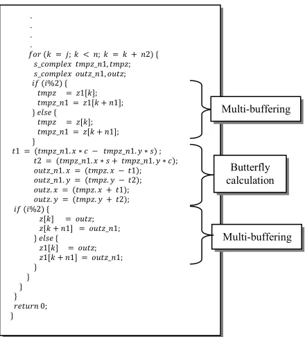
Through this arrangement, the memory accesses are reduced to 2 read and 2 write operations. They can be reduced further using multi-buffering or ping-pong me- mories. Therefore, we use two RAMs z and z1 and we alternate read and write operations. For example, a read operation will be done on z (or z1) while the write opera-tion will be done on z1 (or z):
. . . .
( = ; < ; = + 2) { _ _ 1, ; _ _ 1, ; ( %2) {
= 1[ ]; _ 1 = 1[ + 1]; } {
= [ ]; _ 1 = [ + 1]; }
1 = ( _ 1. ∗ − _ 1. ∗ ) ; 2 = ( _ 1. ∗ + _ 1. ∗ ); _ 1. = ( . − 1); _ 1. = ( . − 2); . = ( . + 1); . = ( . + 2); ( %2) {
[ ] = ; [ + 1] = _ 1; } {
1[ ] = ; 1[ + 1] = _ 1; }
} } } 0; }
Butterfly calculation
Multi-buffering Multi-buffering
By integrating the modifications presented in this sec-tion to the reference C code given in Figure 5, the HLS
[image:6.595.313.533.82.325.2] [image:6.595.59.283.449.639.2]implementation of the FFT can be obtained as shown in
Figure 6.
5. Hardware Synthesis Results
The HLS tool offers different configurations that will have an impact on the hardware generated. For example, the user can specify the desired frequency that may or may not be achieved by the tool depending on the system targeted and the complexity of the C code. As seen in
. . . .
( = ; < ; = + 2) { _ _ 1, ; _ _ 1, ; ( %2) {
= 1[ ]; _ 1 = 1[ + 1]; } {
= [ ]; _ 1 = [ + 1]; }
1 = ( _ 1. ∗ − _ 1. ∗ ) ; 2 = ( _ 1. ∗ + _ 1. ∗ ); _ 1. = ( . − 1); _ 1. = ( . − 2); . = ( . + 1); . = ( . + 2); ( %2) {
[ ] = ; [ + 1] = _ 1; } {
1[ ] = ; 1[ + 1] = _ 1; }
} } } 0; }
Butterfly calculation
Multi-buffering Multi-buffering
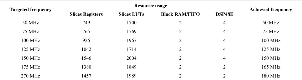
Area reduction in terms of slices and DSP48E blocks can be achieved by increasing the number of clock cycles required to perform the FFT. Hence, for equivalent throughput, it is better to choose a higher operational frequency and a higher number of clock cycles required to perform the FFT. Table 2 shows the hardware usage
of the FFT for a targeted frequency of 150MHz with dif-ferent throughputs. For example, from Table 1, for a
frequency of 75 MHz, the throughput is 10,463. Never-theless, with a frequency of 150 MHz, a better through-put can be obtained using fewer DSP48E blocks (see
Table 2, second row).
this section, increasing the frequency will increase the resources of the hardware generated by the HLS tool. The throughput (number of FFTs that can be done in one second) can also be specified. In order to achieve a high throughput, the HLS tool will parallelize tasks; hence increasing the hardware resources. Finally, the user can specify to implement arrays using block RAMs or look- up tables (LUTs). Hardware implementation results are obtained using Xilinx ISE 12.1 software with either speed or area optimization for Virtex-5 FPGA. The twid- dle factors have been implemented using LUTs but can be also implemented using RAMs. By doing this, it will reduce the total number of slices LUTs but increase the number of blocks RAM/FIFO. Table 1 shows the hard-
[image:7.595.320.538.286.355.2]ware usage of the HLS implementation of FFT with 22-bit data width for different targeted frequencies.
Figure 7 shows the error variation with respect to the
width of the fractional part compared to the reference code shown in Figure 5. The relative error for the FFT is
given using the formula below: One can see a significant increase in terms of logic
slices for 150 MHz operational frequency. This is due to the fact that we have selected optimization for speed in ISE in order to achieve the desired operational frequency after place and route. For frequencies lower than 150 MHz, optimization in terms of area has been selected. For frequencies from 50 MHz to 150 MHz, the total number of clock cycles achieved by PICO to perform the 1024-point FFT is 7168 but for 175 MHz it is increased to 12288 clock cycles. 7168 clock cycles is the minimum latency that can be obtained and is calculated as follow:
99 1023
0 0
[ ][ ] [ ][ ]
1 1
100 1024 [ ][ ]
[ ][ ] [ ][ ]
[ ][ ]
ref HLS
n k ref
ref HLS
ref
X n k X n k
error
X n k
Y n k Y n k
Y n k
(6)
where X and Y are real and imaginary parts respectively. The relative error is calculated for 100 random input signals of 1024 samples each Figure 7 shows that the
relative error decreases linearly as the number of bit for the fractional part increases. For the implementation of the FFT, –40 dB is achieved giving the same results as the Xilinx FFT core. Nevertheless, the user can increase the precision at the expense of hardware usage. For 13 bits, the relative error achieved is –73 dB compared to the reference C code based on double precision floating point operations.
2
*log 2
1024 512*10 1024 7168
latency loading FFT unloading N
latency N N N
lantecy clock cycles
(5)
For frequencies higher than 150 MHz, PICO reduces the tasks’ parallelism of the FFT in order to achieve the desired frequency. This results in an increase of the la-tency and a reduction of the hardware resources. The maximum frequency that can be obtained by PICO is around 270 MHz with a total of 17,408 clock cycles
(1024 ) to compute the FFT.
Never-theless, after place and route, the maximum frequency obtained is 180 MHz due to the FPGA targeted.
3 512 10 1024
Table 3 shows the hardware usage with respect to the
[image:7.595.57.539.606.734.2]width of the fractional part for a desired operational fre-quency of 100 MHz. As expected, the resource usage increases with the number of bit for the fractional part. Nevertheless, the number of blocks RAM/FIFO used is the same. This is due to the architecture of the Virtex-5 FPGA selected.
Table 1. FFT hardware usage for different frequencies.
Resource usage Targeted frequency
Slices Registers Slices LUTs Block RAM/FIFO DSP48E
Achieved frequency
50 MHz 749 1700 2 4 50 MHz
75 MHz 765 1769 2 4 75 MHz
100 MHz 926 1967 2 4 100 MHz
125 MHz 1042 1714 2 4 125 MHz
150 MHz 1546 2004 2 4 150 MHz
175 MHz 1380 1849 2 2 165 MHz
270 MHz 1457 1989 2 2 180 MHz
Table 2. FFT hardware usage for different throughputs.
Resource usage Targeted
throughput Slices Registers
Slices LUTs
Blocks
RAM/FIFO DSP48Es
20926 1546 2004 2 4
12207 1351 1693 2 2
8616 1186 1418 2 2
6658 1161 1404 2 1
0 2 4 6 8 10 12 14 Number of bits for the fractional part
Relative error for different bit sizes for the fractional part –10
–20
–30
–40
–50
–60
–70
–80
R
ela
tive
e
rr
or
in
D
b
[image:8.595.58.285.116.414.2]Figure 7. Relative error for different bit size for the frac-tional part.
Table 3. FFT hardware usage for different fractional sizes.
Resource usage Fractional part
number of bits Slices Registers
Slices LUTs
Block
RAM/FIFO DSP48Es
0 767 1305 2 4
2 809 1474 2 4
4 926 1967 2 4
6 968 2184 2 4
8 1188 2309 2 4
10 1279 2405 2 8
13 1400 2607 2 8
6. Conclusion
In this paper, we have presented hardware considerations that software engineers need to apply when designing hardware modules using HLS tools. As a demonstration, the implementation of a radix-2 FFT unit has been pre-sented. We have shown the different steps to achieve an optimized C code for HLS tools based on an ANSI C
code. Results of the generated FFT for a Virtex-5 FPGA have been presented. FFT has a broad range of appli- cations in digital signal processing, and multimedia. It is a key component that determines most of the design met-rics in many signal processing communication applica-tions. HLS tools facilitate complex algorithms to be real-ized at a higher level. They can reduce the design cycle significantly while successfully generating results very close to handmade HDL design.
7. Acknowledgements
The authors would like to thank the Xilinx, Inc.
(www.xilinx.com) and Synopsys (www.synopsys.com) for their valuable support.
REFERENCES
[1] S. Dongwan, A. Gerstlauer, R. Domer and D. D. Gajski, “An Interactive Design Environment for C-Based High- Level Synthesis of RTL Processors,” IEEE Transactions on Very Large Scale Integration (VLSI) Systems, Vol. 16, No. 4, 2008, pp. 446-475.
[2] S. Ramachandran, “Digital VLSI System Design,” Chap-ter 11, Springer, New York, 2007.
[3] M. Glasser, “Open Verification Methodology Cook-book,” Chapters 1-3, Springer, New York, 2009.
doi:10.1007/978-1-4419-0968-8
[4] E. Casseau and B. Le Gal, “High-Level Synthesis for the Design of FPGA-Based Signal Processing Systems,” In-ternational Symposium on Systems, Architectures, Mod-eling, and Simulation, SAMOS’09, 20-23 July 2009, pp. 25-32.
[5] B. Bailey, G. Martin and A. Piziali, “ESL Design and Verification,” Morgan Kaufmann, San Francisco, Chap- ters 1-6, 2007.
[6] V. Sklyarov and I. Skliarova, “Teaching Reconfigurable Systems: Methods, Tools, Tutorials, and Projects,” IEEE Transactions on Education, Vol. 48, No. 2, 2005, pp. 290-300. doi:10.1109/TE.2004.842909
[7] L. E. M. Brackenbury, L. A. Plana and J. Pepper, “System- on-Chip Design and Implementation,” IEEE Transactions on Education,Vol. 53, No. 2, 2010, pp. 272-281.
doi:10.1109/TE.2009.2014858
[8] J. G. Proakis and D. G. Manolakis, “Digital Processing 4th Edition,” 4th Edition, Prentice Hall, New Jersey, 2006.
[9] Xilinx Inc., “XUPV5 Development Board,” http://www.xilinx.com
[10] Synfora Inc, Website. http://www.synfora.com [11] Synopsys, “Symphony C Compiler,”
http://www.synopsys.com/Tools/SLD/HLS/Pages/Synpho nyC-Compiler.aspx
[12] AutoESL, Website. http://www.autoesl.com [13] Mentor, Website. http://www.mentor.com
[image:8.595.57.288.466.634.2]In-creases Productivity—A Case Study,” IEEE Interna-tional Symposium on VLSI Design, Automation and Test, Hsinchu, 28-30 April 2009, pp. 96-101.
doi:10.1109/VDAT.2009.5158104
[15] Berkeley Design Technology, “An independent Evalua-tion of High-Level Synthesis Tools for Xilinx FPGAs,” http://www.bdti.com
[16] K. L. Man, “An overview of SystemCFL,” Research in
Microelectronics and Electronics, 2005 PhD, Vol. 1, 2005, pp. 145-148.
[17] P. Schumacher, M. Mattavelli, A. Chirila-Rus and R. Turney, “A Software/Hardware Platform for Rapid Pro-totyping of Video and Multimedia Designs,” Proceedings of Fifth International Workshop on System-on-Chip for Real-Time Applications, 20-24 July 2005, pp. 30-33.
doi:10.1109/IWSOC.2005.27
[18] W. Chen (Ed.), “The VLSI Handbook,” 2ndEdition, Chapter 86, CRC Press LCC, Boca Raton, 2007.
[19] S. Van Haastregt and B. Kienhuis, “Automated Synthesis of Streaming C Applications to Process Networks in Hardware,” Proceedings of the Conference on Design Automation & Test in Europe, April 2009, pp. 890-893. [20] P. Coussy and A. Morawiec, “High-Level Synthesis:
From Algorithm to Digital Circuits,” Springer Science + Business Media, Chapters 1, 4, Berlin, 2008.
[21] N. Hatami, A. Ghofrani, P. Prinetto and Z. Navabi, “TLM 2.0 Simple Sockets Synthesis to RTL,” International Conference on Design & Technology of Integrated Sys- tems in Nanoscale Era, Vol. 1, 2000, pp. 232-235. [22] D. L. Jones, “FFT Reference C Code,” University of
Illi-nois at Urbana-Champaign, 1992.