Design of an Asynchronous Switch for Clock Domain
Crossing Interfaces
Hatem M. Zakaria
Electrical Engineering Department,Benha Faculty of Engineering, Benha University, Egypt
Ashraf Mohamed Ali
Department of Electronics andCommunications Sinai University, Egypt
Waleed Elnahel
Department of Electronics andCommunications October University for Modern
Sciences and Arts, Egypt
ABSTRACT
This paper proposes a design of an asynchronous switch interfacing circuit between any numbers of different local clock synchronous domains. The asynchronous switch will generate a slower clock frequency from different local clock modules and moderate the high rated clock domain to slow down its clock frequency without stopping or pausing any clock of them during the data communication phase. The proposed design is implemented using the CMOS 45nm technology of STMicroelectronics and simulated using timed VHDL model (Xilinx ISE Design Suite 12.1). The delay time is required to change the clock frequency is mathematically modeled. It is shown that the switching delay time depends on the number of multipoint communicating domains. The proposed system is designed to use a small number of circuit elements that results in conspicuous improvements in terms of power consumption, throughput, and circuit area.
General Terms
Clock Frequency- Switching Delay, Power Consumption, throughput
Keywords
Switch, Local Clock, Asynchronous, multipoint, circuit area
1.
INTRODUCTION
Modern system on chip (SOC) designs faces an increasing integration densities and large chip designs. Consequently, large chip designs are commonly partitioned into several clock domains. Each distinct synchronous clock domain often uses asynchronous method to connect between different domains. This type of systems is commonly known as GALS (globally asynchronous locally synchronous). Synchronous clock domains based on programmable ring oscillator can be used to change each domain frequency by applying different configurations of set/reset for the C-Muller gates, [1]. GALS design style combine the advantage of both synchronous and asynchronous operations, [2]. The main issue is designing reliable GALS interfaces to eliminate the metastability and single event transient logic domains in deep sub-micron technology. More recent GALS solutions have some focus on reducing EMI, facilitating system integration and providing side channel security. There are three basic techniques used to transfer data safely between different synchronous blocks to handle metastability in GALS system, namely, FIFO buffers, pausible-clock generators, and boundary synchronization.
1.1
FIFO Solution
This solution handles the synchronization problem using FIFO buffers. Designer can use this solution to interconnect synchronous and asynchronous modules and also to construct synchronous-synchronous and asynchronous-asynchronous.
This method can achieve an acceptable data throughput [3], [4], and [5]. Because of data cells (empty/full detector) in FIFO architecture, the silicon area is costly. The advantage of FIFO is that they do not affect the locally synchronous domain’s operation. Many FIFO based designs have been published recently [6], [7] and [8].
1.2
GALS with Pausible Clocking
The main idea of asynchronous wrapper is to generate a stretch signal to stop the activity of both clock (receiver and transmitter). This method is used to solve the problem of synchronization between the two clock domains [9], and [10]. This structure contains inputs and outputs between the locally synchronous modules.
1.3
Boundary Synchronization
Third solution is to attain very reliable data transfer between locally synchronous modules. This method does not affect the inner operation of the locally synchronous blocks during data synchronization at the borders of locally synchronous module [11], and [12].
Our GALS employs a self-timed communication scheme between coarse-grained circuit blocks and combine the following features:
1) All major modules are designed in accordance to proven synchronous clocking discipline.
2) Data exchange between modules strictly follows a full handshake protocol.
3) Each module is allowed to run from its own local clock frequency (and supply voltage), making scaling far more convenient than with the standard synchronous approach, which in accordance contributes to power savings. The paper work is organized as follows. In section 1 an introduction about GALS on-chip networks is presented. A new GALS communication mechanism based on the use of the STRs with asynchronous handshake circuits is proposed in Section 2. Section 3 provides the background, definitions and principles of Self-Timed Rings (STR). Then the idea of synchronizing a point-to-point GALS system is generalized to a multipoint GALS interconnection are presented in section 4 and 5. Experimental results of the design are reported in Section 6 and 7 Finally, Section 8 states the paper conclusions and future works.
2.
GALS SYSTEM INTERFACING
speed of the faster domain on one side through the handshake interfacing on the other side. The main advantage of this method is that it uses asynchronous circuit in securing data communication between different clocks and control the
[image:2.595.153.459.116.330.2]problem of metastability. The importance in this system is that it evades stopping data communication between different clock domains during their synchronization phase of data.
Fig. 1. GALS System Based on Asynchronous Switch.
In Fig. 1 a simplified block diagram of transferring data based on GALS system is shown. It uses ring oscillator and an asynchronous switch to safely synchronize the data transfer by asynchronous handshaking acknowledgement Ack and request Req signals. The com signal is activated in data exchange mode. In communication state, each synchronous module has Asynchronous switch to communicate between any number of clocks from other synchronous modules and its own clock to select the slower clock frequency from them. The detailed
interconnection between the ring oscillator and the asynchronous switch are depicted in following section.
3.
SELF-TIMED RINGS
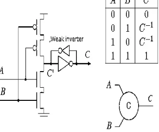
The C-element is the elementary element in asynchronous circuit design, introduced by Muller. C-elements set their output to the input values if their inputs are equal and hold their output otherwise. Fig. 2 depicts a possible CMOS implementation.
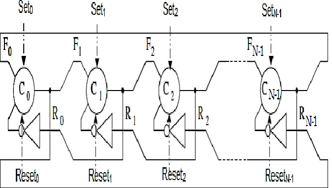
[image:2.595.143.471.465.736.2]Each stage of the self-timed ring (STR) is composed of a C-element and an inverter connected to the input B. The input which is connected to the previous stage is marked F
[image:3.595.144.480.111.301.2](Forward) and the input which is connected to the following stage is marked R (Reverse), C denotes the output of the stage, as shown in Fig. 3.
Fig. 3. A Self-Timed Ring with Set/Reset.
The number of tokens and bubbles will be respectively denoted NT and NB. For keeping the ring oscillating, NT must be an even number; the reader can think about this as the duality of designing the inverter ring by odd number of stages. Each stage of the STR contains either a token or a bubble. NT + NB = N, where N is the number of the ring stages. The oscillation frequency in STR depends on the initialization (number of tokens and bubbles). The oscillation frequency in a self-timed ring can be approached according to the number of token and bubbles by the following formula [13]:
B T rr ff B T rr ff T B ff B T rr N N D D if N N D D if N N , D N N , D R D, where Dff the static forward propagation delay from input F to the output C and Drr the static reverse propagation delay from input R to the output C.The STR can be extended to be Programmable Self-Timed Ring) (PSTR), [1]. In this case, we can control not only STR initialization (i.e. Set/Reset configurations) but also the number of stages. This enables the generation of a widespread range of frequencies [1]. This modeling takes the Charlie effect into consideration to give identical steady state behavior and both are oscillating in evenly spaced mode. Moreover, Charlie effect has a correct behavior of the ring model. In this model a ring stage propagation delay is represented when taking into account the Charlie [14], and [15] and Drafting effects [16], [17], and [18]. The Charlie effect can be defined by the following phenomena "the closer the input event; the longer the propagation time" which appears in the input stage transistors. The Drafting can be defined by the following phenomena "the closer the successive transitions; the shorter the propagation time" which appears on the output stage capacitance. The analytical formulation of Charlie model is expressed by:
With: and
These parameters are noted as:
s … the half separation time between inputs. … the static forward propagation delay. … the static reverse propagation delay. … the amplitude of the Charlie
effect. y … the time between the previous output commutation and the mean input time. A… the duration of the Drafting effect. B … the amplitude of the Drafting effect.
4.
CIRCUIT DESIGN OF A CDC
ASYNCHRONOUS SWITCH
4.1
Asynchronous Switch for Two
Different Clock Domains
disconnected from the MUX input and cuts the connection between the two communicating domains. Therefore, the first
[image:4.595.146.471.93.414.2]clock frequency of ring oscillator is return back.
Fig. 4. Asynchronous Switch Interconnections with the Ring Oscillator.
Fig. 5. Internal Control Switch Circuit.
5.
DEVELOPMENT OF
ASYNCHRONOUS SWITCH
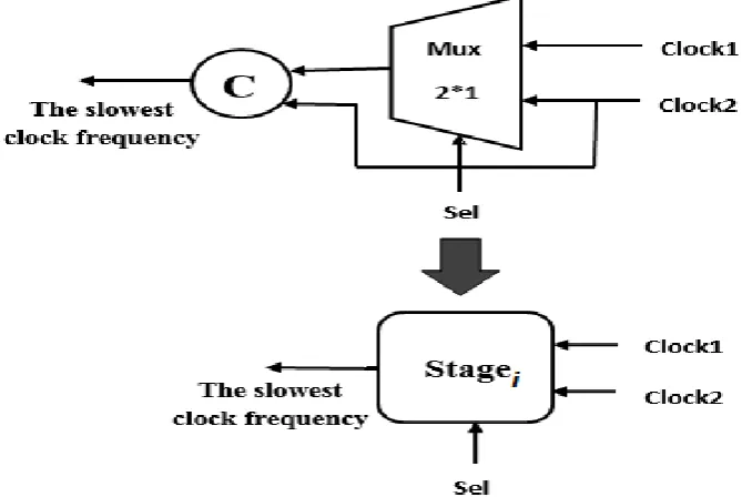
In this section, A previous method is developed for interfacing a point to-multi point communication between the different clock frequencies in a GALS system. Let's consider the Mux connected with C2 shown in the gray area of Fig. 5 as stagei
for synchronizing two clock domains. This design can
communicate with any number of clock domains by cascading set of such stages (MUXs and C-Muller's). For example, while connecting three input clocks domains (one of them is coming from an asynchronous ring and others from normal clocks). In this case, two cascaded stages of the circuit shown in Fig. 6 are used. One more example, when five clock domains are communicating, the design will contain four stages of such circuit shown in Fig. 6.
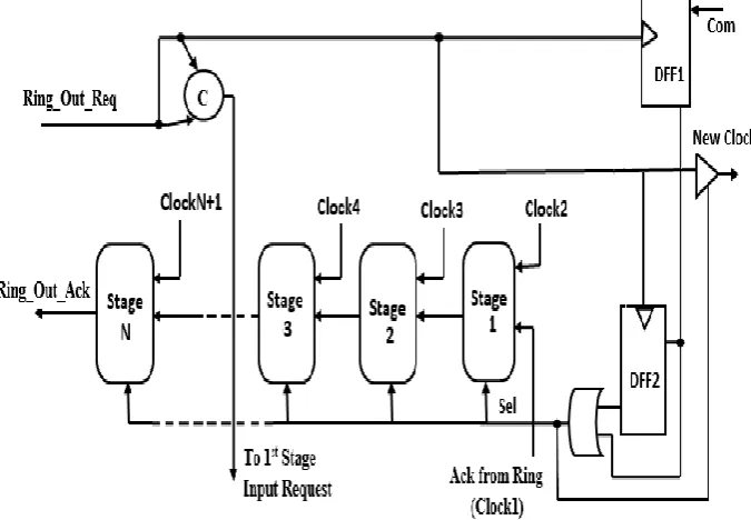
[image:4.595.140.475.518.742.2]The asynchronous switch is shown in Fig. 7. The inputs of the switch are number of handshaking signals of the ring oscillator (Req and Ack) and normal clocks frequency, the output of this switch are two handshaking signals to close the
[image:5.595.138.476.123.357.2]ring oscillator feedback to generate its corresponding clock frequency and the other output is a new clock signal. The new clock is generated only when com signal equals 1 (i.e. we have data exchange).
Fig. 7. Clock Domain Crossing (CDC) Asynchronous Switch Interfacing in a GALS System.
As C-Muller elements are used as a state holding element, it will start to generate any output only when both inputs are equal to 1. When the last clock cycle of our communicating domains is completed, the data synchronization will only start. The inputs of first stage will be clock2 and ACK from asynchronous ring clock1. Given that, the clock signals of the other side communicating module is connected to the GALS network through clock2, clock3, clock4 etc. So that, if com signal changes from 0 to1, the multiplexer sel signal will not be allowed to change 1 except with the complete the clock cycle of our communicating domain by DFFs. The output of first stage will be synchronized between two clocks (one of asynchronous ring and the other of GALS network) and sure the output follow the slower clock frequency of the two clocks with small time delay corresponding to the Charlie effect on C-Muller and this output is the input of the second stage with the clock3 to generate the slower clock frequency of them and
so on until, the new clock is generated from all GALS network and asynchronous ring will be operating with the new clock. Conversely, if com signal changes its state from 1 to 0, the connection between GALS network and asynchronous ring is disconnected and the first clock frequency of asynchronous ring clock1 is return back as sowing in following figures.
6.
SIMULATION RESULTS
[image:5.595.116.504.566.744.2]The asynchronous switch shown in Fig. 7 is implemented on CMOS 45nm technology. Post layout simulation using timed VHDL model has been used to extract the delay information. Fig. 8, is an example where the asynchronous switch is requested to change its state from no communication to data transfer with another synchronous module, then it changed its state to no communication again.
At point A, com signal changes its state from 0 to 1. As a result, the output of two DFF and sel signal are changed to 1 with the next negative edge of clock. The MUX in first stage will be selected clock2 and synchronized with clock1 by C-muller of stage and the output is the slowest clock frequency from inputs. The output of first stage is the input of second stage with clock3. Therefore, the new clock of the output of
[image:6.595.114.517.144.364.2]asynchronous switch will be slower clock in them as depicted in Fig. 8 and the clock1 which come from Asyn. Ring will be changed to a new clock as showing in Fig. 8. At point B, com changes it stage from 1 to 0. In this case, the new clock will be disconnected and the clock1 is return back as before as showing in Fig. 8.
Fig. 9. Timing Diagram of the output of different four clock frequencies.
More examples on this design are shown in Fig. 9 and 10. The four clock domains are inputs to the asynchronous switch as showing in Fig. 9. At point A, the first value of clock1 is 2.322 ns generated from asynchronous ring and clock2 is 40 ns, clock3 is 80 ns, and clock4 is 160 ns. When the com signal is changed to 1, the new clock is generated with the slowest clock of them, which is 160 ns. The clock1 is changed to the
[image:6.595.103.530.449.681.2]new clock (160 ns). The delay needed to generate the new clock is computed in the next section. At point B, the com signal is changed to 0 and the clock1 back to the first value, and the new clock will be disconnected as showing in Fig. 9. Fig. 10, as another example of four different clock domains test case with same scenario.
Fig. 10. Timing Diagram of the output of different five clock frequencies.
7.
DELAY ESTIMATION
The total delay of circuit design in Fig. 7 with asynchronous ring is estimated from Eq. (3). It's extracted from the simulation results as shown in Fig 8, 9, 10 and tables 1, 2, 3. The delay of asynchronous switch depends on the number of stages used and can be expressed in the equation by:
time to synchronize between three different clocks, clock1 is 3.27 ns output from the asynchronous ring, clock2 is 35 ns, and clock3 is 5 ns. In this example, needing the two stages only. The new clock output is the slowest clock from them (i.e. 35 ns), the largest delay time in this case is 0.595 ns according the simulation result from Xilinx ISE 12.1, and according to Eq. (3) equals (0.4+0.195(2-1)) = 0.595 ns. Therefore, the two results from behavioral simulation result and mathematical model of Eq. (3) is the same without any error. In table 2, the largest delay time when the clock2 is the slowest clock is (0.4+0.195(3-1)) = 0.79 ns according to Eq. (3) and the simulation result is the same value. Delay time between five different clocks as showing in table 3 when clock2 is the slowest according to Eq. (3) is (0.4+0.195(4-1) = 0.985 ns and the output from simulation is the same result and so on.However, when clock3 period exists in the second stage and it is the slowest period, the delay estimation in this case is
(0.4 +0.01) = 0.41 which is less than before ns when synchronized between three clocks only as shown in table 1, but when synchronized between four clocks, the delay is (0.4+0.195+0.01) =0.605 ns as shown in table 2, and when synchronized with five clocks, the delay is (0.4+(2*0.195) +0.01) =0.8 as showing in table 3. This is due to the fact that clock rates are checked in a sequential manner. Once the first stage doesn't contain any of the slowest clocks, it acts like a buffer during consequent checks on the steady state behavior. This corresponds to the delay of the C-Muller which is 0.01 ns. While the remaining stages keeps check wither the generated clock is higher than the current input domain clock or not. In general Eq. (3) can be modified to be as follows:
Where Stage i. is the stage order that receives the slowest
clock rate on one of its control switch inputs.
Table 1: The Delay Output from Three Different CDC Domains
Clock1 (Async. Ring) Clock2 Period (ns) Clock3 Period (ns) New Clock (ns) Delay (ns)
3.27 35 5 35 0.595
2.322 4 50 50 0.41
Table 2: The Delay Output from Four Different CDC Domains
Clock1 (Async. Ring) Clock2 Period (ns) Clock3 Period (ns) Clock4 Period (ns) New Clock (ns) Delay (ns)
2.322 60 20 5 60 0.79
2.322 60 160 80 160 0.605
2.27 60 20 80 80 0.41
Table 3: The Delay Output from Five Different CDC Domains
Clock1 (Async. Ring) Clock2 Period (ns) Clock3 Period (ns) Clock4 Period (ns) Clock5 Period (ns) New Clock (ns) Delay (ns)
3.322 120 60 20 10 120 0.985
3.27 60 120 20 10 100 0.8
3.322 20 60 120 10 120 0.605
3.27 20 60 10 120 120 0.41
8.
CONCLUSIONS
In this paper, a new interface design is proposed to be used as a clock domain crossing in NoC-GALS systems that employ many clock domains. The proposed design is especially useful in the growing SoC design field where components of varying characteristics are being integrated on a single chip. The proposed design allows the data to cross clock domain boundaries safely. The design mitigates the communicating modules of the communication overhead and allows them to continue their normal operation while the interface takes care of the transmission. Unlike previously proposed CDC interfaces, the new interface does not necessitate the communicating modules to stop their operation
[image:7.595.150.447.259.594.2]9.
REFERENCES
[1] H. Zakaria, “Asynchronous Architecture for Power Efficiency and Yield Enhancement in the Decananometric Technologies: Application to a Multi-Core System-on-Chip”,PhD Thesis, Grenoble UniversityFrance, 2011.
[2] Ding, W. and Marchionini, G. 1997 A Study on Video Browsing Strategies. Technical Report. University of Maryland at College Park.
[3] D. Chapiro, “Globally-Asynchronous Locally Synchronous Systems”, PHD Thesis, Stanford University, report No. STANCS-84-1026, 1984.
[4] T. Chelcea and S. Nowick, “Low-latency asynchronous FIFO's using token rings”, in Proceedings of the 6th International Symposium on Advanced Research in Asynchronous Circuits and Systems ASYNC '00, pp. 210-220, 2000.
[5] A. Chakraborty and M. Greenstreet, “Efficient self-timed interfaces for crossing clock domains”, in Proceedings of the 9th International Symposium on Asynchronous Circuits and Systems ASYNC ‘03, pp. 78-88, 2003. [6] E. Beigne and P. Vivet, “Design of on-chip and off-chip
interfaces for a GALS NoC architecture”, in Proceedings of the 12th IEEE International Symposium on Asynchronous Circuits and Systems ASYNC '06, pp. 172-183, 2006.
[7] T. Chelcea and S. Nowick, “Robust Interfaces for Mixed-Timing Systems”, in IEEE Transactions on Very Large Scale Integration Systems, pp. 857-873, august 2004.
[8] A. Sheibanyrad and A. Greiner, “Two Efficient Synchronous-Asynchronous Converters Well-Suited for Network on Chip in GALS Architectures”, in Integration, the VLSI Journal, pp. 17-26, january 2008. [9] I. Miro-Panades and A. Greiner, “Bi-Synchronous FIFO
for Synchronous Circuit Communication Well Suited for Network-on-Chip in GALS Architectures”, in Proceedings of the 1st International Symposium on Networks-on-Chip NOCS’07, pp. 83-92, may 2007. [10]R. Ginosar, “Fourteen ways to fool your synchronizer”,
International Symposium on A synchronous Circuits and Systems Async’03, pp. 1-8, 2003.
[11]R. Dobkin, R.Ginosar and C. Sotiriou, “Data synchronization issues in GALS SoCs”, in Proceedings of the 10th International Symposium on Asynchronous Circuits and Systems ASYNC ‘04, pp. 170-180, 2004. [12]J. Muttersbach, T. Villiger and W. Fichtner, “LPractical
design of globally asynchronous locally-synchronous system”, In Proceedings of the International Symposium on Advanced Research in Asynchronous Circuits and Systems ASYNC’00, pp. 52-59, 2000.
[13] K. Yun and R. Donohue, “Pausible Clocking: A First Step Toward Heterogeneous Systems”, In Procedings of International Conference on Computer Design ICCD, pp. 118-123, 1996.
[14] E. Yahya, O. Elissati, H. Zakaria, L. Fesquet and M. Renaudin, “Programmable/Stoppable Oscillator Based on Self-Timed Rings”. In Proceedings of the 15th IEEE Symposium ASYNC '09 , Chapel Hill, USA, pp. 3-12, May 2000.
[15] J. C. Ebergen, S. Fairbanks and I. E. Sutherland, “Predicting performance of micropipelines using Charlie diagrams”, ASYNC’98, in IEEE, San Diego, CA, USA, pp. 238 - 246, April 1998.
[16] V. Zebilis and C. P. Sotiriou, “Controlling event spacing in self-timed rings”, ASYNC’05, in IEEE, New York, USA, pp. 109 – 115, March 2005.
[17] A. Winstanley and M. R. Greenstreet, “Temporal Properties of self timed rings”, CHARM’01, London, UK, Springer-Verlag, pp. 140 – 154, April 2001. [18] S. Fairbanks and S. Moore, “Analog micropipeline rings
for high precision timing”, ASYNC’04, in IEEE, CRETE, Greece, pp. 41–50, April 2004.
[19] A. Winstanley, A. Garivier and M. Greenstreet ,“An event spacing experiment”, in Proceedings of the International Symposium on Advanced Research in Asynchronous Circuits and Systems, ASYNC 02, pp. 47–56, 2002.
[20] H. Zakaria and R. Nawar, "Design of a Self-Timed Data Synchronizer for Crossing Two Different Clock Domains",in Proceedings of the International Journal of Computer Applications
, USA,
pp.17-22, February 2017.[21] Weihua Wang, Jihong Zhao, Hua Qu and Badong Chen, Convergene Performane an Analysis of an Apaptive Kernal Width MCC. International Journal of Electronics and Communications, Vol.76, PP.71-76, 2017.
[22] M.N. Kapetina, M.R. Rapaicy and Z.D. Jelicic, Two Stages Adaptive Estimation of Irrational Linear System, International Journal of Electronics and Communications, Vol.76, PP.111-118, 2018.
[23] H. J. Kim, C. V. Hoof, and R. F. Yazicioglu, "A Mixed Signal ECG Processing Platform with an Adaptive Sampling ADC for Portable Monitoring Application", 33rd annual international conference of the IEEE EMBS., PP. 2196-2199, 2016.