A high power factor rectifier based on buck converter
operating in discontinuous inductor current mode
YANG, Jianbo, ZHANG, Weiping, AL-NAEMI, Faris and CHEN, Xiaoping
Available from Sheffield Hallam University Research Archive (SHURA) at:
http://shura.shu.ac.uk/14286/
This document is the author deposited version. You are advised to consult the
publisher's version if you wish to cite from it.
Published version
YANG, Jianbo, ZHANG, Weiping, AL-NAEMI, Faris and CHEN, Xiaoping (2013). A
high power factor rectifier based on buck converter operating in discontinuous
inductor current mode. Energy and Power Engineering, 5 (4B), 842-849.
Copyright and re-use policy
See
http://shura.shu.ac.uk/information.html
A High Power Factor Rectifier Based on Buck Converter
Operating in Discontinuous Inductor Current Mode
*
Jianbo Yang1, Weiping Zhang2,Faris Al-Naemi1,Xiaoping Chen2
1Materials and Engineering Research Institute (MERI), Sheffield Hallam University (SHU), Sheffield, UK 2Lab of Green Power & Energy System (GPES), North China University of Technology (NCUT), Beijing, China
Email: [email protected]
Received September, 2012
ABSTRACT
By adding a suitable LC filter to the input of a Buck converter, a high-power-factor buck converter is proposed. The converter can operate in the discontinuous-output-current mode operation. A Buck converter in this operation mode features simple control as the constant duty cycle PWM used. The operation condition of the converter is studied. The validity of analysis is verified by Simulation and Experimental results.
Keywords: Discontinuous-output-current; Buck Converter; Power Factor Correction
1. Introduction
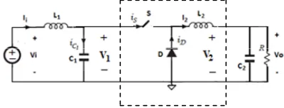
Intensive research has been carried out to improve the power factor of AC/DC converters [1]-[4]. Among the research, it has been reported that by adding a suitable LC filter to the input of a Buck converter to make the converter operate as power factor correction circuit [5] [6]. An example of the converter is presented in Fig. 1. The input capacitor C1 usually has a low enough value
and the voltage across it can be discontinuous. Then a high-power-factor can be obtained by a simple constant duty ratio PWM control. However, the voltage stress across switch(S in Figure 1) and diode (D in Figure 1) imposes major restrictions as the peak value of Vc1 is
very high when Vc1 becomes zero for part of the
switch-ing cycle. In this paper, the Buck converter with LC in-put filter operates in a “discontinuous-outin-put-current” mode. The current of output inductor (L2 in Figure 1)
fells to zero for part of the switching cycle and the volt-age of the input capacitor (C1) becomes continuous. Thus,
the peak value of Vc1 is reduced substantially and switch
voltage stress will be no longer a restriction. Besides the reverse recovery loss of the freewheeling diode (D) is reduced.
The goal of this paper is to give a more comprehensive analysis of Buck converter with the LC input filter oper-ating in DICM. In section 2 of this paper, the principle of DICM is analyzed. Based on the analysis, the character-istics of the converter and the conditions for power factor
correction are studied in section 3. In section 4, the sim-ulation and experimental verifications are given.
2. Operation Principles of DICM
2.1. Operation with Constant Input
As shown in Figure 1, if C1 has large enough value, it
will operate in CCVM and the voltage across C1can be considered constant during one switching cycle. L1 has
large value so that the input current Ii can be
consid-ered as constant. Inductor L2 has low enough value and
operates in DICM. With these assumptions, the converter is the same as the Buck DC/DC converter operating in DCM and the characteristic waveform are presented in
Figure 2. The operation over one switch cycle is as fol-lows:
1) 0 < t < DTs: at t = 0, S is turned on. The current through C1 is IiIo. L2 is charging under constant
voltage (V Vi o).The current through L2 increases
line-arly from zero. Accordingly, the current through C1
de-creases linearly. When I2Ii
2 i
, c1 is positive, C1 is
charging. And when
i
I I is turned to negative, C1 is discharging.
1
c
i
*Project supported by Natural Science foundation of China (N0.
51277004). The Importation and Development of High-Caliber Talents
[image:2.595.322.522.642.718.2]J. B. YANG ET AL. 843
Figure 2. Waveforms for buck converter in DICM.
2) DTs < t < DpTs: at t = DTs, S is turned off. D starts to conduct. L2 is discharging under output voltage. The
current through L2 decreases to zero. C1 is charging with
input current.
3) DpTs < t < Ts: the current through L2 maintains
ze-ro. The output is supported by C2. C1 is still charging by
the input current.
The average voltage across inductor L1, over one
switch cycle, is zero in stationary state. Therefore, the average voltage across capacitor C1 is equal to the input
voltage. As C1 is large enough the changes of voltage
across it during a switch cycle can be disregarded. Thus, the instantaneous voltage across C1 can be considered the
same as the average voltage across it. As a result, the voltage across C1 is the input voltage.
Based on the analysis above, the maximum current through L2 is,
2
2
( i o) s
P
V V DT I
L
(1)
The average current through capacitor C1, over one
switching cycle, is zero in steady state. The input current equals to the average switch current Is over one switch
cycle. 2 2 p i I
I D (2)
Substitution of (1) into (2) gives
2 2
( ) 2
i o s i
V V D T I
L
(3)
The conversion ratio can be defined as o i V k
V
Then an equivalent input resistance i as the ratio
between input voltage and input current is obtained,
R 2 2 2 (1 ) i s L R
k D T
(4)
The equivalent input resistance i is proportional to
L2 and inversely proportional to switching cycle Ts and
duty ratio D.
R
2.2. Operation with Sinusoid Input
The input voltage of the off-line Buck AC/DC converter is a rectified sinusoid voltage.
( ) sin
i p
v t V w ti (5) where wi2 Ti and is the input cycle. Ti
The switching cycle Ts is usually much smaller than the input cycle i. Thus, the input voltage can be con-sidered constant over one switching cycle. Thus, the analysis of the converter with rectified sinusoid input over one switching cycle is the same as the converter with constant input. Simply substitution of (5) into (3), the input current is then
T
2
2
( sin )
( )
2
p i o
i
V w t V D T
i t
L
s
(6)
If Vp sinw ti Vo, the input current can be simplified
as, 2 2 sin ( ) 2 p i i
V w t D T
i t
L
s
(7)
Thus, the input current is proportional to the input voltage when the duty ratio is constant.
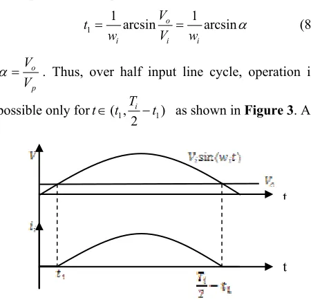
Buck converter operates only when the input voltage is higher than the output voltage. Therefore, (6) is valid only for Vi sinwit Vo When the input rectified
volt-age equals to the output voltvolt-age,
1
1 arcsin o 1 arcsin
i i i
V t
w V w
(8)
o
p V V
. Thus, over half input line cycle, operation is
possible only for ( ,1 ) 2
i T
t t t1 as shown in Figure 3. As
t
[image:3.595.310.535.503.720.2]t
shown in Figure 3, the input current is zero outside the Interval ( ,1 )
2 i T
t t1
)
. This introduces the crossover distortion in the input current. However, the distortion can be accepted if the output voltage is much lower than the peak input voltage.
3. DICM Operation Boundary
The average voltage across inductor L2 is zero over a
switching cycle in steady state. Thus, according to Fig-ure 2,
(V V D V Di o) o( pD (9) Then the conversion ratio can be obtained as,
o
i p
V D
V D (10)
As depicted in Figure 2, for Buck converter under DICM . Thus
1
p
D (V Vo i)D. The conversion ratio has to be larger than duty cycle D to maintain the converter operates under DICM. This restriction is also valid for rectified input voltage. Therefore, with rectified input voltage, the conversion ratio is,
sin
o
p i
V
D
V w t (11)
Then,
sinw ti D
(12)
As the maximum value of sinusoid waveform is 1,
D
must be larger than 1 to maintain the converter operates under DICM. When D smaller than 1, thus for 2 ( , ) 2 i T
t t t2 (13)
where, 2 1 arcsin i t w D
(14)
the converter operates in DCVM [6].
A summarization can be given So far for the operation of the converter. The converter will operate in DICM during the entire input cycle (half-line cycle) when
1
D .
If D1,the converter will operate in DCVM for
2 2 t2t1 t1
( , )
2 i T
tt t where is given by (8). During the
intervals ( ,t t1 2 e converter operates
in DICM. Thus, when
2,
2 2
i i
T T
t
1
) ( t), th
1
D
, the operation of the converter switches between M and DCVM. These
intervals are presented in Figure 4.
DIC
The conversion ratio can be obtained as a function of duty ratio D from the energy balance over half input cycle. The input energy can be calculated as,
2 1 T t 1 2
i t i i
W
v i dt (15)Substitution of (5), (6), (8) into (15), the input energy is obtained as,
2
V D2 2
2
2 2 1
(1 arcsin ) 8
i i s i T T W L
(16)
The output energy over half input cycle is
2 T V 2 i o o W R
(17)
R is load in Figure 1. With consideration of efficiency
η, the energy balance is,
o i
W W (18) Substitution of (16) and (1
eq
7) into (18), a quadratic uation of can be obtained as,
2 2 1
2
2 2 2 1
(1 arcsin ) 0
k D
(19)
where 2 1 2 s L k RT . t t 1 D
,DICM
(a)
t
t
[image:4.595.310.534.357.703.2](b) D1, switching between DICM and DCVM
J. B. YANG ET AL. 845
Ma ot th
con-ve
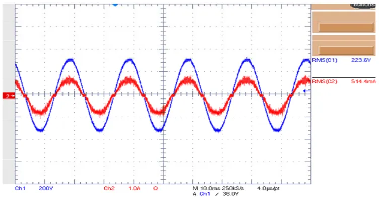
220VAC and the output voltage is 36V. According to the parameters, D1. The converter will operate in DICM during the entire half-line cycle base on the anal-ysis in section 3. The simulation results verify the theo-retical analysis and show that input current will follow the input voltage automatically when Buck converter with an input LC filter operates in DICM with a constant the duty cycle.
tlab can be used to solve (19) and to pl e rsion ratio α as a function of duty ratio D with different parameters k1. The plot is depicted in Figure 5. The
effi-ciency η is assumed to be 0.8. The results in Figure 5
show the boundary D1. When the parts of the curves lie in the area above the boundary, it means
1
D
and the converter operates in DICM. When the ers of the curves are under the boundary, it means that the converter operates between DICM and DCVM. When k1 is smaller, the more parts of the curves
are above the boundary. As k1 is proportional to the L2, it
is in accordance with our sense that the smaller L2
oper-ates in DCM more possibly with constant duty cycle. remaind
4. Results
ions
rried out by Psim to verify the
dis-4.2. Experiments
An experiment circuit was also built and the parameters and the components used is the same as the simulations. The control chip was UC3854AN. The experimental re-sults are in accordance with the simulations. The input power is 125w and the output power is 100w. The effi-ciency is about 80%. The power factor is 0.98.
4.1. Simulat Figures 6 to 15 verify the boundary condition of the
converter operating in DICM. The experiments also prove that the duty cycle D can be a simple constant val-ue to gain a high power factor when the converter oper-ating in DICM.
Simulations were ca
continuous inductor current operation of the circuit. The components used are: L1 = 500u, L2 = 20u, C1 = 220n, C2 = 2000u D = 0.1, R = 13. The input voltage is
0.15 0.16 0.17 0.18 0.19 0.2 Ti me (s)
0
-2
-4 2 4
[image:6.595.62.537.90.285.2]I9 VP17/150
Figure 6. Input voltage and input current (220Vac; 0.52A).
0.15 0.16 0.17 0.18 0.19 0.2
T i me (s) 0
-20 20 40 60 80
[image:6.595.62.537.322.489.2]V20
Figure 7. Output voltage: 36v (ripple: 5v).
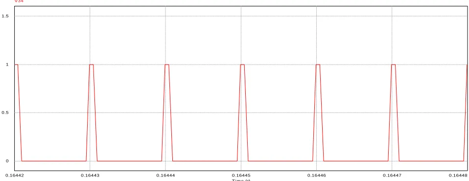
0.16442 0.16443 0.16444 0.16445 0.16446 0.16447 0.16448
T ime (s) 0
0.5 1 1.5
V34
[image:6.595.59.538.529.714.2]J. B. YANG ET AL. 847
0.16442 0.16443 0.16444 0.16445 0.16446 0.16447 0.16448
T i me (s) 0
5 10 15
[image:7.595.53.536.91.261.2]I(L15)
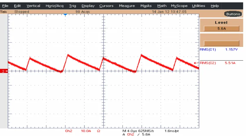
Figure 9. Output inductor current (L2 in Figure 1: DCM).
0.15 0.16 0.17 0.18
T i me (s) 0
50 100 150 200 250 300 350
[image:7.595.61.539.298.485.2]VP18
Figure 10. Input capacitor voltage (C1 in Figure 1: CCM).
[image:7.595.110.486.523.720.2]Figure 12. Output voltage: 36VDC (ripple: 5v).
Figure 13. Output inductor current (L2 in Figure 1) DCM.
[image:8.595.81.514.566.717.2]J. B. YANG ET AL. 849
Figure 15. Constant duty cycle (0.15).
5. Conclusions
The Buck converter with LC input filter operating in DICM can gain a high power factor when the duty ratio maintain constant. Composed to the BOOST PFC con-verter, the Buck PFC converter can obtain an output voltage lower than the peak of the input voltage, which is suitable for the low DC voltage application. The detailed analysis presented in the paper suggested that the Buck converter may switch between DICM and DVCM if
. When 2 1
2
s L k
RT
1
D
is constant, the duty ratio is
proportional to the conversatio
voltage is constant, thus, the duty ratio is actually re-versely proportional to the input voltage.
A 100 w prototype has been built and the results veri-fied the theoretical analysis in this paper
REFERENCES
[1] D. S. Chen and J.-S. Lai, “A Study of Power Correction Boost Converteroperating at CCM-DCM Mode,” in Proc. IEEE Southeastcon, Vol. 93,pp. 6-13.
[2] W. Tang, Y. Jiang, G. C. Hua, F. C. Lee and I. Cohen, “Power Factor Correction with Flyback Converter Em-ploying Charge Control in APEC’93 Rec., pp. 293-298 [3] V. Vlatkovic, D. Borojevic and F. C. Lee, “Input Filter
Design for Power Factor Correction Circuits,” in IE-CON ’93 Rec., Vol. 2, pp. 954-958.
[4] E. X. Yang, Y. Jiang, G. C. Hua and F. C. Lee, “Isolated Boost Circuit for Power Factor Correction,” in IEEE APEC ’93 Rec., pp. 196-203.
[5] Y. S. Lee, “Modeling, Analysis, and Application of Buck uous-Input-Voltage Mode
Opera-nd. Electron., Vol. 12, No. 2, MARCH 1997.
[6] V. Grigore and J. Kyyra, “High Power Factor Rectifier Based on Buck Converter Operating in Discontinuous Capacitor Voltage Mode,” in Proc. IEEE Appl. Power Electron. Conf. Expo., Mar. 1999, pp. 612-618.
Nomenclature
DICM Discontinuous Inductor Current Mode DCVM Discontinuous Capacitor Voltage Mode