3545 Harbor Boulevard
UCOI/L
(RL01/RL02 COMPATIBLE) UNIVERSAL CONTROLLER
TECHNICAL MANUAL
Costa Mesa, California 92626 (714) 662-5600 TWX 910-595-2521
y
Copyright (C) 1983 Emu1ex Corporation
The information in this manual is for information purposes and is subject to change without notice.
Section Section 1 1.1 1.2 1.2.1 1.2.2 1.2.3 1.3 1.3.1 1.3.2 1.3.3 1.3.4 1.3.5 1.3.6 1.3.7 1.4 1.4.1 1.4.2 1.4.3 1.4.4 1.5 2 2.1 2.1.1
TABLE OF CONTENTS
INTRODUCTION
SCOPE 1-1
OVERVIEW 1-1
UC01/L Emulation of RL01 and RL02 1-1
UC01/L Configuration 1-1
SCSI Bus 1-2
FEATURES 1-2
Microprocessor Design 1-2
Packaging 1-2
Self-Test 1-2
Buffering 1-2
Error Correction 1-2
Options 1-3
Configuration Switches 1-3
FUNCTIONAL COMPATIBILITY 1-3
Media Compatibility 1-3
Address Mapping 1-3
Diagnostics 1-4
Operating Systems 1-4
UC01/L CONTROLLER SPECIFICATIONS 1-4
GENERAL DESCRIPTION
CONTROLLER ORGANIZATION RAM Buffer
2-1 2-1
.
,
2.1.2 SCSI Bus and Bus Control Circuitry 2-1 2-5 2-6 2-6 2-8 2-8 2-8 2-8 2-8 2-9 2-9 2-9 2-9 2-9 2-10 2-10 2-11 2-12 2-12 2-12 2-12 2-12 2-13 2.1.3 2.1.4 2.2 2.2.1 2.2.1.1 2.2.1.2 2.2.2 2.2.3 2.2.4 2.2.5 2.2.6 2.2.7 2.2.8 2.3 2.3.1 2.3.2 2.3.2.1 2.3.2.2 2.3.2.3 2.4 2.4.1 2.4.2Q-Bus Interface Microprocessor PHYSICAL DESCRIPTION
Connectors
SCSI Bus Connector Test Connectors Switches
LED Indicator Firmware PROMs Bootstrap PROMs Configuration PROM Address PROM
22-Bit Addressing INTERFACES
SCSI Bus Interface Q-Bus Interface
Interrupt Priority Level Register Address
DCOK and INIT Signals LOGICAL DISK FORMAT
2.4.3 2.4.4 2.4.4.1 2.4.4.2 2.4.4.3
Section 3
3.1 3.2 3.3 3.3.1 3.3.2 3.4 3.5 3.5.1 3.5.2 3.5.3 3.5.4 3.5.4.1 3.5.4.2 3.5.4.3 3.5.4.4 3.6 3.6.1 3.6.2 3.7 3.7.1
3.7.2 I
3.7.3 3.7.4
Section 4
4.1 4.2 4.2.1 4.2.2 4.2.3 4.2.4 4.2.5 4.2.6 4.2.7 4.2.8 4.3 4.3.1 4.3.1.1 4.3.1.2 4.3.2, 4.4 Mapping
Sector or Data Block Format Header Format
Data Field Postamb1e
INSTALLATION
INTRODUCTION INSPECTION
DRIVE PREPARATION Unit Addressing
Data Block Addressing SYSTEM PREPARATION
CONTROLLER SETUP
Controller Address Selection Interrupt Vector Address
Drive Configuration Selection Option Installation
Q-Bus Termination Option
22-Bit Memory Addressing Option Bootstrap PROM Options
Line Time Clock Option CONTROLLER INSTALLATION
Cabling Grounding TESTING
Self-Test
Register Examination
Hardware Formatting Media Diagnostics
PROGRAMMING, AND CONTROLLER REGISTERS
2-13 2-14 2-14 2-16 2-17 3-1 3-1 3-1 3-2 3-2 3-2 3-2 3-4 3-6 3-6 3-6 3-6 3-7 3-7 3-8 3-8 3-9 3-10 3-10 3-11 3-11 3-11 3-12
INTRODUCTION 4-1
PROGRAMMING INFORMATION 4-1
Interrupt Operations 4-1
Seek Operation 4-1
Overlapped Seek Operation 4-2 Data Transfer Operations 4-2 Recovery of Data From Blocks with Bad 4-3
Headers
22-Bit Memory Addressing 4-4
Deleted Commands 4-4
Extended Commands 4-4
OPTION CHARACTERISTICS 4-4
Bootstrap Routines 4-4
Standard Console Bootstrap 4-4
Auto-Boot Sequence 4-5
LTC Option 4-7
4.4.1 4.4.1.1 4.4.1.2 4.4.2 4.4.3 4.4.3.1 4.4.3.2 4.4.3.3 4.4.3 •
.r-4.4.4 4.4.4.1 4.4.4.2 4.4.4.3 4.4.4.4 4.4.4.5 4.4.5 4.4.5.1 4.4.5.2 4.4.6section 5 5.1 5.2 5.2.1 5.2.2 5.2.3 5.2.4 5.2.5 5.2.6 5.2.7 5.3 5.3.1 5.3.2 5.3.3 5.3.4 5.3.5
controller Status Register (CSR) CSR Normal Functions
CSR Extended Functions Bus Address Register (BAR) Drive Address Register (DAR)
DAR During Seek Operation
DAR During Read or Write Command DAR During Get Status Command DAR During write Header Command
(Extended)
Multipurpose Register (MPR) MPR After Get Status Command MPR After Read Header Command
MPR During Read/Write Data Commands MPR During Multipurpose Command
(Extended)
MPR During write Header Command (Extended)
Bus Address Extension (BAE) Register BAE During Read Data atr Write Data
Commands
BAE During Write Header Commands (Extended)
Registers 5, 6, and 7 FUNCTION CODES
FUNCTION CODES STANDARD FUNCTIONS
Write Check Operation - Function Code 1
Get Status Operation - Function Code 2
Seek Operation - Function Code 3 Read Header Operation - Function
Code 4
write Data Operation - Function Code 5
Read Data Operation - Function Code 6
Read Data Operation without Header Check - Function Code 7
EXTENDED COMMANDS
Write Switch Register Command -Function Code 0
Read Firmware Register Command -Function Code 2
Firmware Format Command - Function Code 4
Write Bad Sector File Command -Function Code 6
Transfer SCSI Bus Command Packet without Data - Function Code 10
5.3.6 5.3.7 Appendix A
A.l
A.2
Transfer SCSI Command Packet With 5-7 Data Function Code 12
Reserved Commands - Function Codes 8, 5-7 14, and 16
UCOI/L CONFIGURATION AND OPTION SELECTION INTRODUCTION
CONTROLLER CONFIGURATION
LIST OF TABLES
Table No, Title
Table 1-1 Iomega and RLVll/RLOl/RL02 or 1-4 RLV12/RLOl/RL02 Disk Subsystem
Specifications
Table 1-2 UCOI/L Controller Specifications 1-5 Table 2-1 SCSI Bus Device Interface Pin 2-2
Assignments
Table 2-2 Q-Bus Interface Pin Assignments 2-5
Table 2-4 SCSI Bus Phases 2-10
Table 3-1 UCOI/L Controller DIP Switch Functions 3-3
Table 3-2 Hardware Format Commands 3-12
Table 4-1 Bootstrap Routine 4-6
Table 4-2 Halt Routines 4-7
Table A-I Drives Supported A-I
Table A-2 Drive Configurations A-I
LIST OF FIGURES
Figure No, Title
Figure 2-1 UCOI/L Universal Controller 2-1 Figure 2-2 SCSI Bus, Simplified Diagram 2-3
Figure 2-3 SCSI Bus Physical Path 2-4
Figure 2-4 UCOI/L Universal Controller PCBA, 2-7 Component Side
Figure 2-5 Sector or Data Block Format 2-14
Figure 2-6 Logical Header Format 2-15
1.1 SCOPE
Section 1
INTRODUCTION
This manual provides information related to the capabilities, design, installation, and use of the UCOI/L Universal Controller manufactured by Emulex Corporation. This manual also provides diagnostics and application information.
1.2 OVERVIEW
The UCOI/L Universal Controller is a single printed circuit board assembly (PCBA) designed to be embedded in a Digital" Equipment Corporation (DEC) LSI-II central processing unit (CPU). The UCOI/L controller can be used to interface the LSI-II CPU with any disk mass-memory peripheral device that uses the Small Computer System Interface (SCSI) based on the ANSC X3T9.2 standard.
1.2.1 UCOI/L Emulation of RLOI and RL02
In conjunction with one of several SCSI-compatible disk drives, the UCOI/L controller emulates two DEC RLVll (18-bit address
capability) or RLV12 (22-bit address capability) disk controllers and attached RLOI and RL02 disk drives. The UCOI/L controller includes a BDVll-Compatible Clock Simulator plus bootstrap programmable read only memories (PROMs), and Q-Bus termination resistors. The UCOI/L controller is compatible with all single-ended SCSI devices and and DEC operating systems used on LSI-II CPUs that support DEC RLOI or RL02 disk subsystems. The UCOI/L controller may be configured, by switching, to operate with and map into many different types of SCSI-compatible drives.
1.2.2 UCOI/L Configuration
Emulation of the RLVll/RLV12 provides a convenient controller architecture for a wide variety of modern technology disk drives. The RLVll/RLV12 controller emulation is supported by DEC LSI-II operating systems and is easy to program.
1.2.3 SCSI Bus
The SCSI bus interface can accept data rates up to about four megabytes/second, and allows device independence without requiring system hardware or software modification. The SCSI interface uses logical addressing for all command/data structures. All data are addressed as logical blocks up to the maximum number of blocks in a peripheral device; each device can be interrogated to determine how many blocks it contains.
1.3 PEATURES
The UCOI/L Universal Controller includes seven features that enhance performance and versatility.
1.3.1 Microprocessor Design
The UCOI/L controller design incorporates a unique 8-bit bipolar microprocessor that performs all controller functions. Using the microprocessor reduces the component count, provides high reliability and easy maintainability, and ~nables a single set of hardware to be adapted to a wide range of emulation capabilities through the flexibility of microprogramming. The Emulex UCOI/L Universal Controller achieves functional capability that exceeds performance of emulated DEC controllers by providing enhancement features such as built-in self-test during power-up, built-in disk formatting, and ability to work with drives of various types, sizes and capacities.
1.3.2 Packaging
The UCOI/L is constructed on a single, quad-size, multiple-layer printed circuit board assembly (PCBA) which plugs directly into the Q-Bus in the DEC LSI-II CPU chassis or expansion box. No cabling is required between the CPU and the UCOI/L controller. The UCOI/L controller obtains its power from the chassis in which it is mounted.
1.3.3 Self Test
The UCOI/L controller firmware includes an internal self-test routine which is automatically executed when power is first applied
(power-up mode). This self test exercises all parts of the microprocessor, buffer, and storage-device data logic. It does not test all controller circuitry, but successful execution indicates high probability that the controller is operational. If the controller fails the self test, the red FAULT light emitting diode
1.3.4 Buffering
The UCOI/L controller contains a lK x a-bit high-speed random access memory (RAM) buffer. The RAM buffer is used to temporarily store the contents of the controller's device registers plus a full 5l2-byte block of data from a selected disk sector. This buffering permits multiple Read operations to be performed with a l-to-l data block interlace format. Buffer operations eliminate the
possibility of a data-late condition, and permit the controller to be operated at low bus priorities.
1.3.5 Options
Sockets allow insertion of optional 5l2-word bootstrap PROMs, and Q-Bus termination resistor packs. Dual in-line package (DIP) switch settings allow optional user functions to be selected, and also enable a software-controlled line time clock (LTC). These optional functions are compatible with the functions provided by the BDVll; therefore, no BDVll module is required in the LSI-II system that uses the UCOI/L controller.
1.3.6 Configuration Switches
DIP switches are provided to configure the UCOI/L controller for· various device types, sizes and capacities, Q-Bus addresses, and operating characteristics. Up to 64 possible combinations of drive characteristics can be selected for the eight drive devices handled by the UCOI/L controller.
1.4 FUNCTIONAL COMPATIBILITY
The UCOI/L Universal Controller is compatible with media, address mapping, diagnostics, and operating systems to the extent described
in this subsection.
1.4.1 Media Compatibility
Disk packs formatted with the UCOI/L controller are not media compatible with other Emulex controllers or with RLOI or RL02 disk drives.
1.4.2 Address Mapping
1.4.3 Diagnostics
On LSI-II CPU systems, the UCOI/L controller can run the following diagnostic programs:
o o o o
ZRLGBO ZRLHBO ZRLKBI ZRLMBO
Controller Test No. 1 Controller Test No. 2 Performance Exerciser Bad Sector File Tool
No modification of any of these diagnostic programs is required.
1.4.4 Operating System§
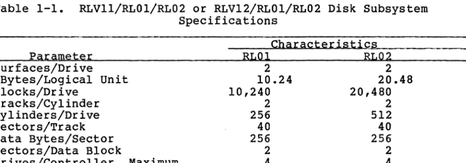
The UCOI/L controller is compatible with all DEC operating systems used on LSI-II CPUs that support DEC RLOI or RL02 disk subsystems. No operating system modifications are required. Table 1-1 lists and describes disk subsystem specifications that are compatible with the UCOI/L controller.
Table 1-1. RLVll/RLOl/RL02 or RLV12/RLOl/RL02 Disk Subsystem Specifications
CharacteristiG~§~ ____ __
Parameter RLOI RL02
Surfaces/Drive 2 2
MBytes/Logical Unit 10.24 20.48
Blocks/Drive 10,240 20,480
Tracks/Cylinder 2 2
Cylinders/Drive 256 512
Sectors/Track 40 40
Data Bytes/Sector 256 256
Sectors/Data Block 2 2
Drives/Cont~er, M~y-m~ __________ ~4 ________________ ~4 __________ _
1.5 UC01/L CONTROLLER SPECIFICATIONS
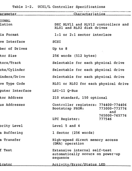
[image:12.618.68.544.341.507.2]Table 1-2. UCOI/L Controller Specifications
- - - -
Paramete~. _ _ _ _ _ _ _ _ _ _ _ _ ~C~..t...e..r_itiiLP..lo.t .... i..loo<c_li!.s _ _ _ _ _--
_FUNCTIONAL Emulation Media Format Drive Interface Number of Drives Sector Size
Sectors/Track Tracks/Cylinder Cylinders/Drive Drive Type Code Computer Interface Vector Address Q-Bus Addresses
Priority Level Data Buffering Data Transfer Self Test
Indicator
DEC RLVll and RLV12 controllers and RLOI and RL02 disk drives
1:1 or 2:1 sector interlace SCSI
Up to 8
256 words (512 bytes)
Selectable for each physical drive Selectable for each physical drive
, Selectable for each physical drive RLOI or RL02 for each physical drive LSI-II Q-Bus
210 standard, 150 optional Controller registers:
Bootstrap PROM: LTC Register: Level 5 and 4
1 Sector (256 words)
774400-774406 773000-773776
and
765000-765776 777546
High-speed direct memory access (DMA) operation
Extensive internal self-test automatically occurs on power-up sequence
[image:13.618.101.555.75.662.2]Table 1-2. UCOI/L Controller Specifications (continued) Parameter
Options
Design PHYSICAL
Mounting Connectors ELECTRICAL
Q-Bus Interface Drive Interface
Power
---Characteristics 512 word bootstrapQ-Bus termination BDVll LTC control 22-bit addressing.
High-speed, bipolar microprocessor that uses 2901 bit-slice components
Any LSI-II Q-Bus quad slot in CPU or expansion box
One 50-pin flat-cable connector
DEC approved line drivers and receivers
Differential line drivers and
receivers. Cable accumulative length to 35 feet.
[image:14.617.52.567.84.499.2]2.1 CONTROLLER ORGANIZATION
Section 2 GENERAL DESCRIPTION
The UCOI/L controller is organized around an 8-bit, high-speed, bipolar microprocessor. A simplified block diagram of the functional elements in the UCOI/L controller is shown in Figure 2-1. The arithmetic logic unit (ALU) and the register file portion of the microprocessor are implemented with two 2901 bit-slice IC components. The microinstruction code is 48 bits long, and the 1024-word control memory is implemented by 12 lK x 4-byte PROMs. 2.1.1
RAM
BufferThe UCOI/L controller incorporates a lK x 8-byte high-speed RAM
buffer which temporarily stores (buffers) the contents of the controller's device registers plus one sector or block (5l2 bytes) of data.
2.1.2 SCSI Bus and Bus Control Ci.~~
The SCSI bus interfaces the UCOI/L controller with the selected drive device. Signals are supplied at 50-pin connector Jl. A simplified diagram of the SCSI bus is shown in Figure 2-2,
Ser ial data bits from the selected dr i ve are converted into eight-bit parallel data characters and transferred to the RAM buffer via the microprocessor. Conversely, parallel bytes accessed from the RAM buffer via the microprocessor are serialized in time with the Servo Clock pulse received from the drive, and sent to the selected drive.
2.1.3 a-Bus Interface
The Q-Bus interface consists of four circuit board edge connectors: A, B, C, and D. These connectors use 48 low-level active signal lines. Two of these lines are unidirectional and 46 are bidirectional. The Q-Bus interface is used for programmed input/output (I/O), CPU interrupts, and data transfers.
2.1.4 Microprocessor
The microprocessor responds to all programmed I/O and executes the I/O functions required for the addressed control register. The microprocessor also controls all direct memory access (DMA)
operations, and transfers data between the Q-Bus data lines and the RAM buffer.
2.2 PHYSICAL DESCRIPTION
The UCOI/L Universal Controller consists of a single quad-sized PCBA which plugs directly into the four Q-Bus connectors in a DEC LSI-II CPU chassis or expansion box. The UCOI/L PCBA is shown in Figure 2-4.
2.2.1 Connectors
In addition to the Q-Bus circuit board edge connectors, which are part of the board substrate, the UCOI/L PCBA contains connectors Jl, J2, and J3.
2.2.1.1 SCSI Bus Co~~tor
The 50-pin flat cable connector, reference designated Jl, at the top center edge of the PCBA is for the SCSI bus cable that interfaces the controller with the first drive device and daisy chains to all drives in the system (up to eight) •
2.2.1.2 Test Connectors
(PHYSICAL LAYOUT PHOTO OR LINE DWG)
2.2.2 Switches
The UCOI/L controller contains six DIP switch packs, reference designated SWl, SW2, SW3, SW4, SW5, and SW6. Each switch is so configured that the ON condition of any switch in the pack occurs when the slide is pushed to the right (toward the number side of the switch pack). DIP switch functions are described in Section 3. Functions occur only for switch-ON (closed) condition; for no description, switch is either open or not used.
2.2.3 LED Indicator
There is an LED indicator mounted between switches SWI and SW3 at the upper-right edge of the board, as viewed from the component side. The LED indicates operating conditions that may have several causes:
a. When the controller is reset (SWl.l ON), or if a Power-Up sequence occurs on the system in which the controller is installed, the controller performs a self test of its internal logic. The self test takes only a fraction of a second, but during self testing the LED is lit. The LED is extinguished after the self test is completed.
b. If self test fails, the LED remains continuously lit and the controller registers remain inaccessible. The controller must be removed and replaced or repaired before the system can be functional.
c. If no drive is attached to the SCSI bus, or if a drive attached to the SCSI bus fails to respond to status polling, the LED blinks ON and OFF with a period of approximately one second. The LED remains extinguished as long as drive(s) attached to the SCSI bus respond to status polling.
NOTE
The UCOI/L controller continuously
polls drives assigned to it to determine drive status at all times.
d. The LED illuminates during data transfers to and from any drive. This LED illumination provides a visual indication of system activity.
2.2.4 Firmware PROMs
number on the top of each PROM IC is an Emulex part number which identifies the unique program pattern of the PROM. The PROMs are used to emulate specific DEC equipment functions. When inserting PROMs in sockets, the ID numbers on the top of the PROMs must be in the same sequence as the PROM numbers on the circuit board beside each respective socket; e.g., ID 9 must be inserted in PROM 9. 2.2.5 Bootstrap PROMs
Two PROM sockets are provided for installation of optional Bootstrap PROMs. Socket UlOl receives PiN 014x and socket Ul03 receives PiN 015x. These sockets are in middle of second row of ICs (from bottom) •
2.2.6 Configuration PROM
PROM configuration is determined by installing the proper Configuration PROM in socket U64 (next to SW4 in right-center of circuit board).
2.2.7 Header PROM. socket switch 2.2.8
Address PROM
addressing is determined by the configuration of the Address The Address PROM is installed in PROM socket Ul04. This is near middle of second row of ICs (from bottom) next to SW5.
22-Bit Addressing
Socket U126 (bottom row below switch SW5) is available for installation of a 2908 IC if 22-bit addressing is required by the system. when this IC is installed, switch SW2.7 must be set to the ON position (see Section 3).
2.3 INTERFACES
The UCOl/L controller interfaces with selected disk drive or tape drive via the SCSI bus flat cable and 50-pin connector Jl. It interfaces with the LSI-II CPU via the Q-Bus.
2.3.1 SCSI Bus Interface
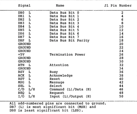
Table 2-1. SCSI Bus Device Interface Pin Assignments
Signal Name Jl Pin Number
DBO L DBI L DB2 L DB3 L DB4 L DB5 L
DB6 L
DB7 L DBP L GROUND GROUND GROUND +5V GROUND GROUND ATN L GROUND BSY L
ACK L
RST L MSG L
SEL L C/D L/H REQ L
I/O L/H
Data Bus Bit 0
Data Bus Bit 1 Data Bus Bit 2 Data Bus Bit 3 Data Bus Bit 4 Data Bus Bit 5
Data Bus Bit 6
Data Bus Bit 7
Data Bus Bit Parity
Termination Power Attention Busy Acknowledge Reset Message Select
Command (L)/Data (H)
Request
Input (L)/Output (H)
All odd-numbered pins are connected to ground. DB7 (L) is most significant bit (MSB) and
DBO is least significant bit (LSB).
2 4 6 8 10 12 14 16 18 20 22 24 26 28 30 32 34 36 38 40 42 44 46 48 50
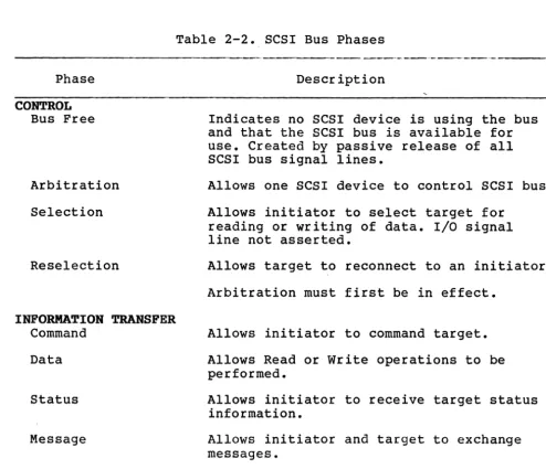
The SCSI bus transfers parallel information between the initiator and the target (see Figure 2-3). It is designed for intelligent peripheral devices.
[image:23.618.67.539.104.497.2]Table 2-2. SCSI Bus Phases Phase
CONTROL Bus Free
Arbitration Selection
Reselection
INFORMA~ION TRANSFER Command
Data Status Message
Description
Indicates no SCSI device is using the bus and that the SCSI bus is available for use. Created by passive release of all SCSI bus signal lines.
Allows one SCSI device to control SCSI bus. Allows initiator to select target for
reading or writing of data. I/O signal line not asserted.
Allows target to reconnect to an initiator. Arbitration must first be in effect.
Allows initiator to command target. Allows Read or Write operations to be performed.
Allows initiator to receive target status information.
Allows initiator and target to exchange messages.
- - - -
-
--
---When the SCSI bus is between two phases, the bus signals are restricted by the following limitations:
a. The BSY, SEL, REQ, and ACK signals cannot change. b. The C/D, I/O, MSG, and DATA signals may change.
c. The ATN and RST signals may change if certain ATTENTION and RESET conditions are met.
2.3.2 Q-Bus Interface
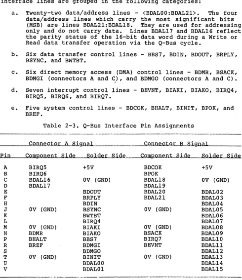
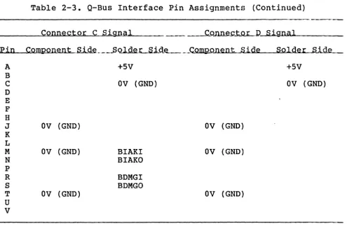
[image:24.620.49.544.62.487.2]connector C. Q-Bus interface pin assignments are listed and described in Table 2-3. The CPU, memory and I/O devices ,use these lines for control, data, and address information. The Q-Bus interface lines are grouped in the following categories:
a. Twenty-two data/address lines - <BDALOO:BDAL2l>. The four data/address lines which carry the most significant bits
(MSB) are lines BDAL2l:BDAL18. They are used for addressing only and do not carry data. Lines BDAL17 and BDAL16 reflect the parity status of the l6-bit data word during a Write or Read data transfer operation via the Q-Bus cycle.
b. Six data transfer control lines - BBS7, BDIN, BDOUT, BRPLY, BSYNC, and BWTBT.
c. Six direct memory access (DMA) control lines - BDMR, BSACK, BDMGI (connectors A and C), and BDMGO (connectors A and C).
I
d. Seven interrupt control lines - BEVNT, BIAKI, BIAKO, BIRQ4, BIRQS, BIRQ6, and BIRQ7.
e. Five system control lines - BDCOK, BHALT, BINIT, BPOK, and BREF.
Table 2-3. Q-Bus Interface Pin Assignments
---________ =C=o=n=n=e=c=t=o~r~A~S~i~g~n~a-l ______________ ~C=o=n~n~e_c~tqr B Signal
&P~i~n~ __ ~C~o~m~p=o=n~e~n=t __ S_i~d~e ____ S=o~l~d~e~r~S_~~de _____ C=om~p~o-n_eun~t __ S~i_q~e __ ~S~o_l~d_e.r __ S_i~d_e A B C D E F H J K L M N P R S T U V BIRQS BIRQ6 BDAL16 BDAL17
OV (GND) OV (GND) BDMR BHALT BREF OV (GND)
+SV OV (GND) BDOUT BRPLY BDIN BSYNC BWTBT BIRQ4 BIAKI BIAKO BBS7 BDMGI BDMGO BINIT BDALOO BDALOl BDCOK BPOK BDAL18 BDAL19 BDAL20 BDAL2l
ov
(GND)ov
(GND) BSACK BIRQ7 BEVNT OV (GND)---
- -
[image:25.620.62.553.121.688.2]Table 2-3. Q-Bus Interface Pin Assignments (Continued)
A B C D E F H J K L M N P R S T U
V
Connector C Signal
ov
(GND)OV (GND)
OV (GND)
+SV OV (GND)
BIAKI BIAKO BDMGI BDMGO
_ _ C=O~t;,QL.J),--""S,"",i~ght.Jn ... a .... l~ _ _ _ _ Solder Side
+SV OV (GND)
OV (GND) OV (GND)
OV (GND)
All signals, except BDeOK and BPOK, are low active.
2.3.2.1 Interrupt priQLj~_LeveL
The UCOI/L controller is hardwired to issue level-4 and level-S interrupt requests. The level-4 interrupt request line is needed for compatibility with either an LSI-II or LSI-ll/2 CPU.
2.3.2.2 Register Address
The register address and the number of registers assigned to the UCOI/L controller are decoded by the Address PROM, installed in PROM socket Ul04 (see paragraph 2.2.7). The available user-select-able options are determined by the settings of configuration DIP switch SWI (see Section 3).
2.3.2.3 DCOK and INIT Signals
[image:26.621.62.558.75.398.2]2.4 LOGICAL DISK FORMAT
The logical disk format involves mapping the system in such a way that the software corresponds with logical addresses on physical devices.
To the system software, the UCOI/L controller/dr i ve subsystem appears to be formatted exactly as an RLOI or RL02 drive. Actually, the controller firmware multiplies the cylinder, track, and sector components of a standard disk drive header address to obtain a numerically sequenced block address (same as a 5l2-byte sector on a disk drive), so that the UCOI/L controller can operate drives in
any combination by merely addressing sequential data block numbers. The possinbility of a 1:1 correspondence between a logical address and a physical address is extremely unlikely.
The LSI-II Q-Bus has two card slots that can be used to interface with one DEC RLVll or RLV12 controller or with two Emulex UCOI/L controllers. One RLVll controller (18-bit address capability) can control up to four RLOI drives, each of which has 10.24 megabytes of storage, or up to four RL02 drives, each of which has 20.48 megabytes of storage. One RLV12 controller can control the same number and types of dr i ves, except it has 22-bi t address capability; therefore, both the RLVll and RLV12 controllers are capable of interfacing with peripheral devices that can provide up to 81.92 megabytes of storage.
The Emulex UCOI/L controller is equivalent to two RLVll or RLV12 controllers. When two UCOI/L controllers are installed in the Q-Bus, the CPU detects the same interface as it would experience with four RLVll or RLV12controllers. Since each UCOI/L controller can control up to eight RLOl- or RL02-type drives, two UCOI/L controllers can control up to 16 RLOl- or RL02-type drives that provide 327.68 megabytes of storage. Thus, the Emulex system supports up to four times the storage capacity as the DEC system can support in the same allotted Q-Bus interface.
2.4.1 Media Organization
2.4.2 Mapping
Depending on the type and capacity of the media, up to eight logical units may be mapped on the physical drive. The UCOI/L controller can control a maximum of eight logical dr ive units distr ibuted on up to, but not more than eight physical disk drives.
NOTE
A logical drive unit may not be mapped across a physical drive unit boundary. 2.4.3 Sector or Data Block Format
Each sector or data block contains a detached two-word header and a 256-word data field. The header field is terminated with two vertical check characters and the data field is terminated with a 32-bit ECC. The controller attempts corrections only on the data. field, never on the header. Each field is preceded by at least 11 bytes of zeros and an eight-bit SYNC byte. Each sector is organized as shown in Figure 2-5.
---Sector Length 562
Bytes Bytes Bytes Bytes Bytes Bytes Bytes Bytes Bytes Bytes Bytes Bytes Bytes Bytes Bytes Bytes Bytes Bytes Bytes Bytes Bytes Bytes Bytes Bytes Bytes Bytes Bytes Bytes Bytes Bytes Bytes Bytes Bytes Bytes Bytes Bytes Bytes Bytes Bytes Bytes Bytes Bytes Bytes
-Preamble Sync Header CRC Preamble Sync Data Field ECC Recovery- - - - ---- --- - - -
--- ---17*--------8----
---17*---- ---512---- -4- ---4*---*Values shown are minimums which apply to most Winchester-type units; however, these values may vary to accommodate different physical drive types and are determined by configuration PROM data.Figure 2-5. Sector or Data Block Format 2.4.3.1 Header Format
The header is the address of a 512-byte block of storage in the peripheral device. System software can read the logical header by
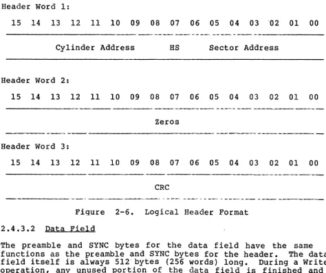
The header preamble is used to synchronize the Phase Locked Oscillator (PLO) in the drive to the data on the media. The SYNC byte is used by the controller to synchronize with the data bytes and their boundaries, and by the drive to synchronize with the phase of the data. The logical header format is shown in Figure 2-6. For the physical header format word organization, the user should see the SCSI interface manual because the word organization structure is different for the header and data fields of each command or function.
Header Word 1:
15 14 13 12 11 10 09 08 07 06 05 04 03 '02 01 00
, _ . _
-Cylinder Address HS Sector Address
Header Word 2:
15 14 13 12 11 10 09 08 07 06 05 04 03 02 01 00
-_._----
--- - -
--
-~-Zeros
---
----,-Header Word 3:
15 14 13 12 11 10 09 08 07 06 05 04 03 02 01 00
---_.
__
[image:29.615.60.535.222.619.2]._--CRC
Figure 2-6. Logical Header Format
2.4.3.2 Data Field
2.4.3.3 Postamble
3.1 INTRODUCTION
Section 3
INSTALLATION
This section describes the step-by-step procedure for installation of the UCOI/L Universal Controller in an LSI-II system. The following list is an outline of the procedure. Each step in the list correlates to a second-level heading in this section; i.e., item 1, Inspect the UCOl/L, procedure is described in paragraph
3.2.
1. Inspect the UCOI/L
2. Prepare the SCSI controller 3. Prepare the drives
4. Prepare the LSI-II 5. Configure the UCOI/L 6. Install the UCOI/L
7. Route the drive I/O cables 8. Run the diagnostics.
3.2 INSPECTION
Emulex products are shipped in special containers designed to provide full protection under normal transit conditions. Immediately upon receipt, the shipping container should be
inspected for evidence of possible damage incurred in transit. Any obvious damage to the container, or indications of actual or probable equipment damage, should be reported to the carr ier company in accordance with instructions on the form included in the container.
3.3 SCSI CONTROLLER PREPARATION
Unpack, inspect, and install the SCSI controllers as instructed by manufacturers. These controllers interface the SCSI bus with the drives as shown in Figure 3-1.
Figure 3-1. SCSI Bus System Components, Simplified
3.4 DRIVE PREPARATION
Unpack, inspect, and install system disk drives or tape drives as instructed by manufacturers. Position and level them in their final places before beginning the UC01/L controller installation. This positioning enables needed length and routing of system I/O cables to accurately determined. To simplify daisy-chain cable installation, drives should be immediately adjacent to each other1 side-by-side, or stacked in standard EIA.or RETMA equipment racks. 3.4.1 Unit Addressing
3.4.2 Data Block AgdLe~g_
A data block on a disk drive is equivalent to a sector on a disk drive. All addressing is made to data blocks (not sectors) which are numbered in sequence on an addressed drive device. The user is not concerned with data block address computation because the conversion is automatically made by the microprocessor circuitry in the UCOI/L controller. For correct data block count settings, see Configuration Selection in Appendix A. The exact method different drive manufacturers use to determine a data block (or sector) count may differ. For corrrect procedure, see manufacturer's manual.
3.5 CPU PREPARATION
To install the UCOI/L controller and associated dr i ves, the inter ior of the LSI-II CPU must be made accessible to the installer. Use the following procedures:
a. Power down system and place main AC circuit breaker at rear of cabinet in OFF position. Verify AC POWER indicator remains lit.
b. Slide CPU out of cabinet and remove top cover.
c. Tilt card cage up. Access to card-cage conectors, CPU interior, and other modules should be available.
3.6 UCOl CONTROLLER CONFIGURATION
Controller configuration must be established before it is installed on the Q-Bus in the LSI-II CPU chassis. Configuration setup is made by setting switches in DIP switch packs SWl, SW2, SW4, SW5, and SW6. DIP switch functions are listed and descr ibed in applicable tables in this section.
3.6.1 Controller Address Selection
All Q-Bus controllers have a block of several command and status registers throOugh which the LSI-II system can command and monitor the controller. These registers are sequentially addressed, beginning with a starting address assigned to the particular controller; i.e., the UCOI/L Universal Controller.
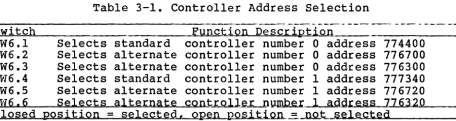
Table 3-1. Controller Address Selection ~S~wAi~t~c~h~ _____________________ -£F~u~n~c~ion Description
SW6.1 Selects standard controller number 0 address 774400 SW6.2 Selects alternate controller number 0 address 776700 SW6.3 Selects alternate controller number 0 address 776300 SW6.4 Selects standard controller number 1 address 777340 SW6.5 Selects alternate controller number 1 address 776720 SW6,6 Selects alternate cont~~u~ .. 1 adgress 776320 Closed position
=
selected, open position=
not selectedThe starting address for the UC01/L controller's Q-Bus registers is selected by DIP switch SW6.n (see Table 3-1). For example, the normal starting address of 774400 for emulated controller number zero is obtained by placing switch SW6.1 in the ON position. Alternate starting addresses of 776700 or 776300 are obtained by setting switch SW6.2 or SW6.3 ON, respectively. The starting addresses for emulated controller number one are 777340, 776720, and 776320, which are set by switches SW6.4, SW6.5, and SW6.6, respectively. Only one switch must be ON for each emulated controller; i.e., DO NOT set switches SW6.4 and SW6.5 ON at the same time, but switches SW6.3 and SW6.4 can be ON at the same time because they affect different emulated controllers. UC01/L controller component locations are shown in Figure 3-2.
3.6.2 Interrupt Vector .AQ.gr~.p.-§.
Two switches in DIP switch pack SW2 are used to select the vector address for each of the two emulated controllers on the UC01/L controller PCBA. These switches and their functions are listed and described in Table 3-2.
Switch SW2.1
SW2.2
Table 3-2. Interrupt Vector Address Selection
- - - - ---
-~--Function Desc~~Q~n~ ______________ ___ Selects interrupt vector address for emulated controller number 0
Open
=
standard vector address of 160 selected Closed=
alternate vector address of 370 selectedSelects interrupt vector address for emulated controller number 1
Open
=
standard vector address of 214 selected [image:34.620.66.536.76.201.2]3.6.3 Drive Configuration Selection
The phrase "Drive Configuration Selection" means the process by which the UCOI/L controller can be configured to use a particular type of physical drive in performing the RLOI or RL02 emulation. That is, a particular set of physical drives is available and the UCOI/L controller must be made aware of what type(s) of physical drives is or are to be used in the system. In the UCOI/L controller, DIP switches SWl.l through SW6.6 are used for that purpose. Configuration PROMs are used in conjunction with certain switches in DIP switch packs SW2 and SW4. These switches and their functions are listed and described in Table 3-3.
Table 3-3. Drive Configuration PRO~ Address Selection Switches Switch
SW2.8 SW4.1 through SW4.7
Funct iOJ'L.P~~t j,g.t_i.Qll ___________ _
Must be closed. Provides LSB of configuration PROM selection. Used with SW4.1 through SW4.7 closed.
Must be closed. Used with SW2.8 closed. SW4.7 provides MSB of configuration PROM selection. SW4.1 through
SW4.6 provide remainder of configuration PROM selection _ _ _ _ --=a.."d~s poj,nter bits. ___________ _
The configuration PROM contains blocks of instructions for
configuring the emulation of each emulated controller on the UCOI/L controller PCBA and the SCSI controllers with associated disk drives. The configuration PROM address selected by the
configuration select switches in Table 3-3 contains a microcode which determines the following elements:
a. SCSI controller (disk formatter) address b. Disk drive address
c. Disk drive type - RLOI or RL02
d. Disk drive capacity (number of data blocks) e. SCSI data block size (optional).
For any other configuration PROM address selected, a different configuration microcode would be produced to accommodate the different system components. Any of the configuration PROM address selection switches could be placed in the closed (ON) or open (OFF) position so that up to 256 different configuration microcodes that could be stored in the configuration PROM could 'be pointed to and selected. At the present design stage, only one configuration microcode has been stored in the configuration PROM; therefore, only one configuration PROM address is selectable by the
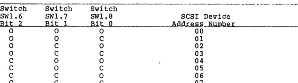
3.6.4 SCSI Deyice Adgress
Switches SWI.6, SWI.7, and SWI.8 are used to select anyone of eight possible SCSI bus addresses that the UCOI!L controller is to use to establish its identity in the system.
SWI.6
=
SCSI device address bit 2 (MSB) SWI.7 = SCSI device address bit ISWI.8
=
SCSI device address bit 0Available SCSI device address identities are listed and described in Table 3-4.
Table 3-4. SCSI Device Address Selection Switches
-,-
--~'--~-Switch Switch Switch
SW1.6 SWI.7 SWI.8 SCSI Device
Bit
2
Bit I Bit 0 A9-9.Le..§.!L.NWDbe r0 0 0 00
0 0 C 01
0 C 0 02
0 C C 03
C 0 0 04
C 0 C 05
C C 0 06
C C C 07
3.6.5 Selection of Miec~llan~ous Switcbable Qp~_qting FunrtioM. This subsection has so far described functions in which the states of two or more DIP switches are coordinated to select or produce a desired condition. Most of the DIP switches are used alone to select, enable, or disable some controller, bus, or disk drive function or emulation. Some of the available DIP switches are not used or have not yet been assigned discrete functions. The remaining DIP switches are listed and descr ibed in Table 3-5. Functions are described in a positive format; i.e., to cause the function to happen, the closed (ON) condition is implied, unless otherwise specified.
Switch SWI.I
Table 3-5. Unassisted DIP Switch Functions Function Description
[image:38.623.61.543.253.388.2]Table 3-5. Unassisted DIP Switch Functions (continued) Switch SWl.l (cont'd) SWl.2 SWl.3 SWl.4 SWl.5 SW2.3 SW2.4
-
- - - - , . _ -- - - - ,
.
-Function Description
the self-test function to be performed by the UCOI/L controller as soon as the Reset operation is finished
(see paragraph 2.2.3, cause a). The Reset feature is normally used only dur ing servicing to clear and initialize the UCOI/L controller after a major malfunction of the UCOI/L controller.
Not used.
Not used.
Normally open. Closed only during serv1c1ng of the UCOI/L controller. When closed, causes the UCOI/L controller to automatically perform Seek operations, during execution of Write or Read commands, by using logical header address data to identify cylinder and track. This function is especially useful when hand-loading Write or Read commands because it saves time and eliminates need for user to issue Read Header and Seek commands separately.
When closed, Write Locks all drives at power-up. Write Lock prevents previously written data on drive media from being written over and lost. Although this Write Lock feature protects and preserves valuable data, the drives in the system become Read-only devices and cannot be written to or edited. In effect, the drives are then a storage library that is not likely to need changing or updating. To re.tain Write/Read capability on one or more drives in the system, SWl.5 should remain open and the extended Write Switch Register command (function coce 0) should be used to Write Lock specific drives only (see paragraph 5.3.1 and Figure 5-1).
Alternatively, switch SWl.5 can be left closed at power-up and after. Then Write Lock on system drives could be disabled, as required, by using the extended Wr i te Switch Register command to leave only specific drives in system in the Write Locked condition.
Not used.
Normally open. When closed, causes UCOI/L controller to change drive selection time-out period on SCSI bus from normal 250 microseconds to 250 milliseconds. This drive selection time-out period is the maximum time the UCOI/L controller is able to wait for a response when attempting to select a physical disk drive. When SW2.4 is open, the UCOI/L controller uses 250 microseconds for the drive selection time-out period.
---Table 3-5. Unassisted DIP Switch Functions (continued) _S~w_i~t=c~h~ __________________ ~F=u_n~c_tjQn Description
SW2.4 This switch is useful when servicing the UCOI/L
(contrd) controller and should NOT be left closed during normal
SW2.5 SW2.6
SW2.7
SW3.1 Through SW3.B SW4.B
SW4.9
operation, because the longer drive selection time-out period would seriously degrade system operation.
Must be open at ALL times.
Normally open. ~Vhen closed, the arbitration sequence that is normally performed automatically by the UCOI/L controller is disabled.
SW2.6 may be used in future configurations to accommodate SCSI controllers (disk formatters) that are NOT
compatible with all of the SCSI bus requirements.
When closed, causes each of the two controllers on the UCOI/L PCBA to emulate a DEC RLV12 controller that has 22-bit addressing capability. To function un 22-Lit bus, insert an AMD290B IC in IC socket U126 to provide the line drivers for four more address lines. The 22-bit addressing provides DEC LSI-ll/23 and LSI-ll/23 PLUS CPUs with access to four megabytes of memory storage capacity. Switch SW2.7 should be open when UCOI/L controller is to be used in system that emulates the DEC RLVII controller (lB-bi t addressing) and when the UCOI/L controller is installed in LSI-II CPUs that are not LSI-ll/23 or LSI-ll/23 PLUS models.
(Not yet assigned any functions)
Normally open. If closed, the time duration of the SCSI Reset pulse that is generated by the UCOI/L controller is changed from the normal 25 microseconds to less than 10 microseconds.
SW4.B may be used in future configurations to accommodate SCSI controllers (disk formatters) that are NOT
compatible with all of the SCSI bus requirements. For the present configuration, closing SW4. B would ser iously
impair proper operation of the UCOI/L controller. When closed, enables Line Time Clock (LTC) option
[image:40.623.48.554.50.729.2]Table 3-5. Unassisted DIP Switch Configurations (continued) Sw itch __ _ _ _ _ _ j'~I1~t.iQJL.oeEiCr i.p-ti QU. _ _ _ ~
SW4.9 Before the LTC can be used, the CPU must be configured to (cont'd) enable that feature. On the LSI-II CPU and LSI-ll/02 CPU,
remove jumper W3 (BEVNT Line Enable). On the LSI-ll/23 CPU, remove jumper W4 (BEVNT Line Enable). The LTC switch on the CPU front panel must also be set in the ON position.
SW4.9 When using the UCOI/L controller wi t.h the Rs':'r cpf-~rotJ.I·.S
(cc,[!t'd) f::ystem, lbe L':'(' opU,on I~Lst f_'f..' CFF (EF4.S 0Pd:). ,:...·le CFL,
tc\,E:'iier, shoeld always be configured to enable the LTC option.
SW4.10 When closed, disables bootstrap PROM (address 765000 or 773000). Address 765000 is automatic bootstrap start address which tries all devices. Address 773000 interrogates for bootstrap device address via CRT.
SWS.l
The UCOI/L controller responds to the bootstrap addresses whether or not the bootstrap PROMs are installed in the
IC sockets UIOI and UI03 on the UCOI/L controller. Closing SW4.10 prevents the UCOI/L controller from responding to bootstrap addresses; therefore, bootstrap programs, routines, and/or sequences contained in the UCOI/L controller can be bypassed by the user so that other bootstrap programs in other system components, which may have the same bootstrap program addresses, can be accessed as required.
Bootstrap PROM 'options are fully explained in paragraph 3.6.6.3 and the bootstrap program routines are detailed
in paragraph 4.3.1.
When closed, causes the UCOI/L controller to perform parity checks on data lines of the SCSI bus and to abort
operations in which parity errors are found. This switch should be used to automatically check parity on SCSI bus for better data integrity. It should not be used if the
device on the SCSI bus does not generate a parity bit.
For devices that generate parity bit, when this switch is
closed and a parity error is found, the parity error is
reported as either a hard data error or as an OPI error. Although the operation is automatically aborted, because such errors are non-recoverable errors, it can be retried.
-Table 3-5. Unassisted DIP Switch Configurations (continued) Switch
SW5~2
SWS.3 SWS.4 SW5.S SWS.6
Not used.
Must ALWAYS be open for proper operation of UCOI/L controller.
Must ALWAYS be closed for proper operation of UCOI/L controller.
Not used.
Must ALWAYS be open for proper operation of UCOI/L controller.
3.6.6 Option Installation
There are a number of other UCOI/L controller options that can be selected by the user. They are placed in effect by physically installing the option on the PCBA, or by setting the appropriate DIP switches.
CAUTION
Some manufacturers of Q-Bus backplanes omit 22-bit addressing capability and use the four lines that would be assigned for such addressing as power lines. In such systems, the 2908 IC should not be installed in IC socket U126 because that IC and possibly other circuitry would be destroyed by heat. Also if the UCOI/L controller is to be used as Q-Bus terminator in a system that has power
connected to lines BDAL18 through BDAL2l, pins 1, 4, 5, and 14 should be cut in the
terminator resistance pack installed in IC socket U128. Cutting these pins prevents excessive power dissipation.
3.6.6.1 Q-Bus Termingtjp~p~LQn
[image:42.620.57.542.111.305.2]These three resistor networks may be ordered from Emulex, or the user may use equivalent terminating resistance networks such as BOURNS PIN 76l-5-R18l/39l.
CAUTION
Some manufacturers of a Q-Bus backplanes omit 22-bit addressing capability and use the four lines that would be assigned for such addressing as power lines. In such systems, the 2908 IC should not be installed in IC socket U126 because that IC and possibly other circuitry would be destroyed by heat. Also· if the UCOl/L controller is to be used as Q-Bus terminator in a system that has power connected to lines BDAL 18 through BDAL 21, pins 1, 4, 5 and 14 should be cut in the terminator resistance pack installed in IC socket U128. Cutting these pins prevents excessive power dissipation.
3.6.6.2 Twentytwo-Bit Memory Addressing Option
The UCOl/L controller can include the 22-bit memory addressing option. The option kit is Emulex PIN SC02l3l02, which consists of a single AMD 2908 IC installed in socket U126. Programming instructions for this option are included in Section 4.
3.6.6.3 Bootstrap PROM Options
These options are firmware routines that load the sytem memory with software that is stored on the disk. The routines are executed by the LSI-II, LSI-ll/02 or LSI-11/23 CPUs. The option kit is Emulex PIN SC02l30l, which consists of two PROMs. The PROM labeled 015x is installed in IC socket UlOl, and the PROM labled 014x is installed in IC socket Ul03. Programming instructions for these options are included in Section 4.
The Bootstrap option has two sections, Standard Console Bootstrap Routine, and Automatic Bootstrap Sequence (Auto-Boot). The Standard Console Boostrap Routine is entered by the CPU at address 773000, DEC's conventional starting address. The Auto-Boot Sequence is entered at address 765000.
The LSI-ll/23 may be configured to take advantage of either the Standard Console Bootstrap routine or the Auto-Boot routines. This CPU also requires that power-up Mode 2 be selected (install jumper W6 and remove jumper W5 on the CPU PCBA). The bootstrap starting address, llowever, is selected by using jumpers WB through WIS. To select the Standard Console Bootstrap routine, install WB. This jumper causes the microprocessor to default to starting address 773000. To use the Auto-Boot option, remove jumper WB, WIO and W12; then install jumpers W9, Wll, W13, Wl4 and WIS.
3.6.6.4 Line Time Clock OptiQn
The Line Time Clock (LTC) option allows program control of the LTC function. This control is enabled by setting DIP switch SW4.9 ON. Programming instructions for this option are included in Section 4.
Before the LTC can be used, the CPU must be configured to enable that feature. On the LSI-II CPU and LSI-II/02 CPU, remove jumper W3 (BEVNT Line Enable). On the LSI-ll/23 CPU, remove jumper W4
(BEVNT Line Enable). The LTC switch on the CPU front panel must also be set to the ON position.
When using the UCOI/L controller with the RSTS operating system, the LTC option must be off (SW4.9 open). The CPU, however, should always be configured to enable the LTC option.
3.7 CONTROLLER INSTALLATION
The UCOI/L controller can fit into any Q-Bus quad slot on the LSI-II backplane. If the resistor networks of the Q-Bus Termination option are installed (see paragraph 3.6.6.1), the UCOI/L controller should be installed in the quad slot which is to provide termination at the end of the Q-Bus; i.e., in the last quad slot of the Q-Bus that is furthest from the first quad slot in the Q-Bus.
If the Q-Bus Termination option is not installed, the UCOI/L controller may be assigned to any desired quad slot, because i t uses the LSI-II four-level interrupt scheme that performs distributed interrupt arbitration.
CAUTION
To avoid potential circuit damage, always turn computer power OFF before installing or removing any PCBA.
of the connector before attempting to firmly seat it in the connector. When properly aligned in connector, press extractor handles on each upper corner to firmly seat.
3.7.1 Cabling
Typical subsystem cabling for the controller and drives is shown in Figure 3-4.
The 50-pin connector of the SCSI bus cable is plugged into connector Jl at the top center of the UCOI/L controller. The other end of the SCSI bus cable is plugged into I/O connector on the first drive. If more than one drive is used, the other drives are daisy chained. Most drives have two I/O connectors that are identically wired one-to-one, so that daisy chaining can be easily accomplished. The last drive on the daisy chain should have a terminator installed. The terminator should be supplied by the drive manufacturer. The terminator is generally plugged into one of the two paired daisy-chain connectors on the drive. Sometimes a ground wire, emerging from the terminator assembly, must be connected to the drive to provide a ground return for the resistors in the terminator assembly. Pin 1 of connector Jl on the
controller is on the left when viewing the omponent side of the controller. Pin 1 of the cable connector has a notch on the connector body to identify it. Twisted pairs of wires in the flat cable have brown-brown twist followed by red-brown twist on pin 1 edge of cable. The cable normally exits to the rear of the CPU chasis in which the controller is installed.
NOTE
Connector Jl is not keyed and can be physically reversed in the header. No damage can result from reversed cable connecton, but the subsystem cannot function.
3.7.2 Grounding
For proper computer system operation, all components must have a common Earth ground; i.e., a reliable DC ground connection to the logic ground of the computer, and separated from AC ground. The ground connection should be 1/2-inch braid (preferably insulated) or AWG number 10 or larger. The grounding wire may be
daisy-chained between drives. If the drive has a switch or a jumper which connects the logical signal ground to the cabinet ground (DC ground to AC ground), that connection should be removed when the drive is placed in the On-Line mode with the controller. The DC-AC ground interconnect shoule be used only when performing local off-line diagnostic tests and maintenance on the drive only.
NOTE
3.8 TESTING
Testing involves self-test, register examination, hardware formatting, and diagnostics.
NOTE
The register addresses mentioned in the following paragraphs are IS-bit
addresses. For system devices that use 22-bit addressing, add 17000000 to obtain the correct address for each register; e.g., register address 774400 becomes 17774400.
3.8.1 Self-Test
When power is applied to the CPU, that power is also simultaneously applied to the UCOI/L controller. Since the UCOI/L controller derives its power from the Q-Bus interface with the CPU, the controller automatically executes a built-in self test. The self test is not executed with every INIT signal from the Q-Bus, but only at power-up time. If the self test is successful, the LED on the top edge of the controller becomes extinguished or flashes. The LED flashes when the controller cannot properly address one drive after successful self-test execution. Such flashing can occur if SCSI bus cable is not properly connected, a drive is not powered up with a unit select code plug, or two drives have identical unit select code plug. Steady illumination of the LED indicates the controller failed the self test and cannot be addressed from the
cpu.
3.8.2 Register ExaminatiQn
After power up of CPU and noting LED on controller is not steadily lit, a quick check should be made to verify that all controller registers can be read from the Gomputer console. The Control status Register (CSR) 774400 should contain 000201 if the controller and drive 0 are both in the Ready state.
3.8.3 Hardware FQr_m~ttiJ).gJte(Ua
The controller can format the disk or tape media by writing headers and bad block file data in all data blocks of the media. This formatting command does not verify the data or the headers. For example, if the sytem contains disk drives which are on line, the disk formatting should occur in the following event sequence:
b. Select drive to be formatted by depositing drive number in bits 09 and 08 of CSR, 774400. Bit 02 must also be set simultaneously.
c. Examine CSR contents. Bit 15 (Error) should be logic 0 and bit 01 (Drive Ready) should be logic 1.
d. Deposit a number to be used as pack identification (ID) in Multipurpose Register (MPR) , 774406.
e. Deposit 1000018 in Bus Address Register (BAR), 774402, to enable Extended command set.
f. To start formatting, deposit in CSR (774400) a hardware Format command for appropriate drive as defined in Table 3-6. Activity LED at top of controller, next to DIP switch SWl, should flash while formatting operation is in progress, when LED is completely extinguished, Format operation is done.
Table 3-6. Hardware Format Command
3.8.4 Diagnostics
Driye No.
o
1
2 3
Command 34004 34404 35004
.J.5
W.L _____ _
To verify proper operation of the entire systen, run the following DEC RLOI/RL02 diagnostics:
o ZRLGBO o ZRLHBO o ZRLMBO o ZRLKBI
Controller Test No. 1 Controller Test No. 2 Bad Sector File Tool
RLOI/RL02 Performance Exerciser
Without the programmable clock, the diagnostic~ skip some sections which time drive operations; including those operations that would fail because the physical drive being used is either faster or slower than the real RL02 drives.
[image:48.620.75.544.81.448.2]Section 4 PROGRAMMING, AND CONTROLLER REGISTERS
4.1 INTRODUCTION
This section describes programming techniques, option
characteristics, and controller registers. Programming information reveals how various operations are handled. Option characteristics descr ibes details of LTC function and bootstrap routines. The controller registers subsection explains the function of each bit in each controller register during performance of commands. Since there are more commands than there are registers, each of the eight registers in the controller generally contributes to the
performance of several functions.
4.2 PROGRAMMING INFORMATION
This subsection explains Interrupt and Seek opera,tions, DatQ Transfer lI0per~tions, error correction and recovery, 22-bit memory addressing, and special commands.
4.2.1 Interrupt Opera~iQ~
If the Interrupt Enable (IE) and Controller Ready (CRDY) bits in the CSR are both set (logic 1), the controller can request an Interrupt operation. The IE bit is set or reset (logic 0) by the software. It is also reset by the Initialize (INIT) condition. The CRDY bit is set by the software when a function is done, by an error flag when an error is detected, or by the INIT condition. CRDY can also be set by the software to cause the controller to start a function (negative GO bit). The Interupt Vector Address for controller number one is 160, unless alternate 370 is selected by DIP switch SW2.l. The Interrupt Vector Address for controller number two is 214, unless alternate 374 is selected by DIP switch SW2.2. The normal priority level for the RLVll Q-Bus is BUS REQUEST 5. The Q-Bus connectors for the RLVll/RLV12 controller, which the Emulex UCOI/L controller replaces, uses this normal priority level.
4.2.2 Seek Operation
The Seek operation is performed in the following e~ent sequence:
a. Issue Read Header command to drive, then wait for IE or CRDY signal.
b. Check for error Flag.
c. Read header word from MPR.
d. Calculate difference and direction for Seek operation.
e. Move difference word to DAR.
f. Issue Seek command to drive and wait for Seek operation to be indicated completed by Drive Ready (DRDY) bit 00 in CSR set.
g. Check error flag again.
A software system that optimizes positional latency would keep current data block address inforamtion in core so that steps b, c, and d of the foregoing event sequence would be unnecessary.
4.2.3 Overlapped Seek Operationa
Since the controller becomes ready and interrupts as soon as a Seek command is issued, it is possible to issue Seek commands to other drives on the SCSI bus while the first drive is seeking. When any Seek operation is completed, however, no Interrupt condition occurs; therefore, the Data Transfer command should be issued to the dr i ve that needs the shortest Seek time. As soon as all required Seek commands have been issued, the drive which first completes its Seek operation can imme(1iatel~{ perform its commanded Data Transfer operation, and issue an Interrupt signal when done.
4.2.4 Data Transfer Op..eJ:atio_ns
A Data Transfer operation ;~ the verformance of a Read or Write command. The user should not attempt to do a Write operation on a Write Protected (or write Locked) drive.
Data Transfer operations are conducted via direct memory access (DMA) facility. The UCOI/L controller (number one or number two) provides 256 words of first in-first out (FIFO) random access memory (RAM) buffering; which, like the DEC RLVll/RLV12 controllers, prevents data-late conditions from occurring. Transfers of data to memory (Read operations) are initiated only after the entire data block (sector) has been read. Transfers of data to media (write operations) are initiated only after an entire data block has been loaded into the FIFO RAM buffer.
a. Load Bus Address Register (BAR) with address if first memory location whose contents are to be transferred.
b. Load Device (Disk) Address Register (DAR) with address of first media (disk) location whose contents are to be transferr·ed.
c. Load Word Count portion of MPR with two's complement of number of words to be transferred.
d. Issue Read Data command or Write Data command, then wait for Interupt signal or test for Drrve Ready (DRDY) status condition.
e. Check for error flag.
Other drives in the system could perform Seek or Data Transfer operations during times between issuance of seek commands and the issuance of Read or write commands.
4.2.5 Recoyery of D9.tll . ...ll:..onLJllQS:KELW.i.t.h a~d_ae.ader.s.
Function Code 7 (see description of bits 03:01 of CSR), Read Data without Header Check, is provided to allow recovery of data from data blocks whose h~aders have beome unreadable. If constant HNF or HCRC errors are encountered in a particular data block so that data cannot be recovered by a standard Read command, use the following procedure:
a. Perform successive Read Header commands until data block which precedes data block with bad head is found.