Path Optimization for Electrically Inspecting
Printed Circuit Boards with Alignment Marks
Hideki Katagiri, Qingqiang Guo, Hongwei Wu, Hiroshi Hamori, and Kosuke Kato
Abstract—In inspections of printed circuit boards (PCBs), a test probe has to be moved to a number of PCB wiring patterns in some order. This paper considers path optimization for minimizing a total path length of testing PCBs arrayed on a plane. Due to the miniaturization of PCBs, the procedure of “alignment” has been recently needed in order to know the exact position of each wiring pattern before each of PCB wiring patterns is electrically tested. Therefore, there is a precedence constraint that alignment marks of a wiring pattern have to be captured by a camera before a test probe is moved to the exact position of the wiring pattern. This paper shows that the problem to be solved can be formulated as a precedence-constrained traveling salesman problem (TSP). An efficient heuristic algorithm is proposed to solve the problem with a practically reasonable time. The proposed algorithm is installed into real PCB inspection machines that have been widely sold in the world. Cost reduction effects for PCB inspection factories are discussed.
Index Terms—Printed circuit board (PCB), inspection path optimization, alignment marks, precedence-constrained travel-ing salesman problem, heuristic algorithm
I. INTRODUCTION
P
Rinted circuit boards (PCB) have been used in almost all electric devices. Therefore, productive efficiency of PCBs is a very important issue. There are many of previous studies on optimization techniques for PCB manufacturing processes such as assembly operations [1], [3], [8] and drilling processes [2]. On the other hand, optimization techniques for PCB inspections have not been sufficiently developed so far except for some studies on multi-chip module substrate testing [7], [10].In production process of PCBs, various wiring patterns are etched on PCBs. PCB inspections, which are done through pattern tests of wiring, are very important processes in PCB manufacturing in order to enhance the reliability of produced PCBs. At the same time, efficiency of PCB inspections directly influences the productive efficiency of PCBs.
Due to the miniaturization of electronic devices, the line pitch of wiring on PCBs recently has become narrower rapidly. In order to deal with such narrow pitch of wiring on PCBs, a new inspection method including so-called alignment operation has been recently used, and the method has been brought to mainstream in PCB electric inspections. However, there is no article on optimization related to the new PCB inspection method including alignment processes. In this study, we tackle a path optimization problem which is to minimize a path length of testing wiring patterns on each PCB sheet. As will be shown later, the problem to
H. Katagiri is with Graduate School of Engineering, Hiroshima Univer-sity, Japan, e-mail: [email protected]
Q. Guo and H. Wu are with Graduate School of Engineering, Hiroshima University, Japan
H. Hamori is with OHT Inc., Japan
K. Kato is with Hiroshima Institute of Technology, Japan
be solved can be formulated as a precedence-constrained traveling salesman problem (TSP) or a generalized pickup and delivery TSP.
Our goal is not only to propose a solution algorithm but also to install the proposed algorithm to real PCB inspection machines which are to be used in the real world. The efficiency and applicability of the proposed algorithm is strictly checked through experiments using benchmark instances based on real PCB wiring patterns. Thus, we shall place emphasis on developing a fast heuristic algorithm which can obtain a good approximate optimal solution with a practically reasonable time. From a practical viewpoint, we also discuss the cost reduction effect for PCB makers or PCB inspection factories through the proposed algorithm.
II. ELECTRICALPCBINSPECTION
A. PCB inspection jig and inspection method
In production process of PCBs, various wiring patterns are etched on PCBs. When a certain problem happens in forming wiring patterns, PCBs may include some defects such as open (disconnection) defects and short defects.
[image:1.595.367.484.473.563.2]In order to electrically test wiring patterns on PCBs, a test jig, called a probe jig, is used. Probe jigs have many of very small pins, as shown in Figure 1. The diameter of pins is about 40∼130 µm.
Fig. 1. Probe jig with pins
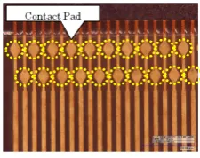
On the other hand, many of wirings on PCBs have bulged parts, called contact pads, as shown in Figure 2. The diameter of contact pads is about 100∼300µm.
Fig. 2. Contact pads in a PCB
[image:1.595.368.481.641.730.2]pins into contact pads of wirings, as shown in Figure 3. In this paper, we deal with the situation that pins of a probe jig correspond one-to-one with contact pads on a PCB wiring pattern.
Fig. 3. Continuity test of a PCB wiring pattern via a probe jig
B. Necessity of alignment via a camera
To exactly conduct the PCB wiring pattern test, each pin must hit the corresponding contact pad. On the other hand, due to the miniaturization of electronic devices, the line pitch of wiring on PCBs recently has becomes narrower rapidly. Therefore, it is more difficult to bring all the pins of a probe jig into contact with their corresponding contact pads.
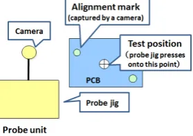
In order to deal with such a narrow pitch of wiring on PCBs, a new inspection method including so-called align-ment operations has been recently used in PCB inspections. In such an inspection method, there is one or two alignment mark(s) for each of wiring patterns. Through the image capturing of alignment marks, inspection machines obtain the information on the exact position (coordinate) of each wiring pattern, which enables a probe jig to properly press onto a PCB wiring pattern so that all the pins of the probe jig can properly hit the corresponding contact pads. Figure 4 shows a wiring pattern with two alignment marks. A camera used for capturing alignment marks is integrated with a probe jig, as shown in Figure 4. We call such a unit (a probe jig with a camera) “a probe unit.”
Fig. 4. Alignment points and test position
Thus, there are two steps in PCB wiring pattern test; the first step is the alignment, and the second step is the test. There is a precedence constraint that alignment marks of a wiring pattern must be captured via the camera before the wiring pattern is tested by a probe jig.
C. Non-optimized inspection path in the present inspection system
In PCB inspections, a large number of PCB sheets are inspected per day. Each of PCB sheets consists of many of
the same wiring pattern which are arrayed in a plane, as shown in Figure 5. Figure 5 shows an example of a PCB sheet which consists of 4 wiring patterns (2×2). In general, the number of the same wiring pattern arrayed in one PCB sheet is around between 4 and 200.
Since the number of PCB sheets to be inspected per day is more than 1,000, even if the amount of reduced time for completing the inspection of a PCB sheet is several percent, the total reduced inspection time a day or a month is significant, which brings a great effect on cost reduction or on productive efficiency of PCBs. Therefore, optimization of inspection paths is considerably worth being studied.
[image:2.595.339.513.246.351.2]In order to consider inspection path optimization problems, we use the concept of graph network in which a probe unit visits alignment marks and test positions.
Fig. 5. PCB sheet (4 patterns)
Without loss of generality, we regard the reference point of the probe unit as the center of the probe jig. In the existing PCB inspection system, inspection paths were not optimized. Figure 6 shows the inspection order that the existing inspection system visits the alignment marks and the test position for the PCB sheet shown in Figure 5.
Fig. 6. Visiting order by the existing inspection system
In the previous inspection system, a probe unit firstly moves to the alignment mark located at the upper left, and then visits only alignment marks in order. After all the alignment marks are visited, the probe unit moves to the nearest test position from the lastly visited alignment mark, and visits only test positions in the inverse order of alignment marks that were already visited. However, not all the alignment marks are necessarily visited before each of test positions is visited. Therefore, the previous inspection paths are not optimal.
III. MATHEMATICAL PROGRAMMING-BASED MODELING AND HEURISTIC ALGORITHM
[image:2.595.354.505.474.553.2] [image:2.595.101.241.522.620.2]with alignment marks can be formulated as a precedence-constrained TSP.
[image:3.595.352.499.54.173.2]To illuminate the readers’ understanding, we utilize an example shown in Figure 5. When alignment marks are captured by the camera of a probe unit, the camera must be moved to alignment mark A in Figure 7. This operation can be achieved by moving the reference point of the probe unit (the center of the probe jig) to vertex A′. Thus, the move of the camera of the probe unit to A is equivalent to the move of the reference point of the probe unit (the center position of the probe jig) to A′.
Fig. 7. Position of the reference point of the probe unit when alignment markAis captured by a camera
[image:3.595.98.243.201.292.2]In a similar manner, we transfer all the positions of alignment marks, as shown in Figure 8.
Fig. 8. Vertices to be visited by a probe unit
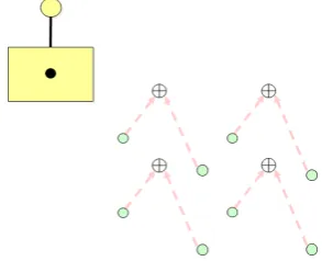
By considering such a graph in which all the positions of alignment marks are transferred, all the inspection paths are regarded as the cycles in which each of vertices shown in Figure 8 must be visited once in some order by the probe unit.
For the sake of visibility of graphs, we give Figure 9 in which the pictures of PCBs are deleted, In this figure, dotted lines represent precedence orders, which means that two alignment marks of each wiring pattern must be visited before the corresponding test position of the wiring pattern is visited.
Figure 10 shows the inspection path corresponding to the previous visiting order shown in Figure 6. As described before, in Figure 10, firstly all the alignment marks are visited, and secondly all the test positions are visited. In other words, a set of alignment marks and that of test positions are completely divided when inspection paths are made in the previous inspection system.
However, it is not necessary to visit all the alignment marks before test positions. In this sense, it is apparent that previous inspection path (or previous visiting order) is not optimal. Actually, the optimal path is shown as Figure 11.
[image:3.595.353.501.211.329.2]Fig. 9. Vertices to be visited by the reference point of the probe unit
Fig. 10. Previous visiting order
In contrast to the previous non-optimized inspection path shown in Figure 10, the optimal inspection path (Figure 10) does not include the crossing of edges in the path. The optimal inspection path length is 4.2 % shorter than the previous non-optimized inspection path. The reduced amount of the path length is not so large because this problem size is very small. However, as will be shown later, the reduced amount is several tens of percent in real instances.
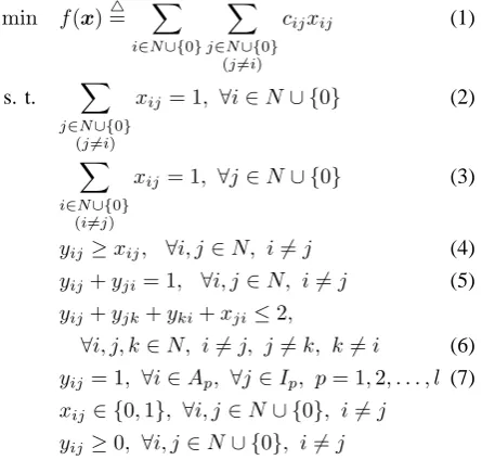
B. Integer programming-based problem formulation Here, we formulate PCB inspection path optimization problem as a precedence-constrained TSP based on the model proposed by Sarin et al. [14]. We use the following mathematical notation throughout this subsection and the next subsection:
{0}: Initial point of a probe unit
B: Index set of wiring patterns on each PCB sheet defined by {1,2, . . . , l}
Ap: Set of alignment marks of pth PCB (p∈B) Ip: Set of test positions ofpth PCB (p∈B) N: Set of all points to visited by a probe unit
defined by N=∪l
p=1(Ap∪Ip)
eij: Edge between vertices iandj (i, j∈N∪ {0}) E: Set of all the edgeseij, ∀i, j∈N∪ {0} cij: Length ofeij (eij ∈E)
In this paper, we introduce two types of decision variables xijs andyijs as follows:
xij = {
1 ifj is visited immediately afteriis visited 0 otherwise
yij =
[image:3.595.97.241.371.489.2]Fig. 11. Optimal inspection path
Decision variablexijis used to represent inspection paths,
namely, construct a path by connecting all edges withxij=
1.
On the other hand, yij is used to express precedence
constraints among vertices corresponding to alignment marks and test positions. In contrast toxij, even ifyij = 1, vertex j is not necessarily visited immediately after vertex i is visited. This corresponds the fact that an test position is not necessarily visited immediately after an alignment mark is visited even if there is a precedence constraint between the test position and the alignment mark.
Then, the problem to find an optimal inspection path for testing all the wiring patterns on a PCB sheet is formulated as the following precedence-constrained TSP [14]:
min f(x)△= ∑
i∈N∪{0} ∑
j∈N∪{0} (j̸=i)
cijxij (1)
s. t. ∑
j∈N∪{0} (j̸=i)
xij= 1, ∀i∈N∪ {0} (2)
∑
i∈N∪{0} (i̸=j)
xij = 1, ∀j∈N∪ {0} (3)
yij ≥xij, ∀i, j∈N, i̸=j (4)
yij+yji= 1, ∀i, j∈N, i̸=j (5)
yij+yjk+yki+xji≤2,
∀i, j, k∈N, i̸=j, j̸=k, k̸=i (6) yij = 1, ∀i∈Ap, ∀j∈Ip, p= 1,2, . . . , l (7)
xij∈ {0,1}, ∀i, j∈N∪ {0}, i̸=j
yij ≥0, ∀i, j∈N∪ {0}, i̸=j
where (1) represents the total moving distance of the in-spection path. Constraints (2) and (3) express flow balance constraints, which means that there exists only one vertex with which each vertex connects in the path. Constraint (4) is the constraint that if j is visited immediately after i is visited (xij = 1), then i must precede j (yij = 1), and
(5) represents the constraint that for any two nodes i, j, either i or j precedes the other node. Constraint (6) is a sub-tour elimination constraint, where xji is added in the
left-hand side to strengthen the constraint, which is effective to reduce the computational time. Constraint (7) expresses the constraint that alignment marks of a wiring pattern must be visited before the corresponding test position of the wiring pattern is visited.
Since the formulated problem is a 0-1 integer program-ming problem, solvers for mathematical programprogram-ming such as CPLEX and Gurobi can be used to solve the problem. However, computational time rapidly increases with increas-ing size of problems. In the case of 2 alignment marks, when the number of wiring patterns on a PCB sheet is beyond 10, solvers cannot obtain the optimal solution within a practically reasonable computational time. Furthermore, since our goal is to install the proposed algorithm into real inspection machines, from the viewpoint of cost reduction, it is not good to use solvers which are free for academic use. Therefore, we construct a heuristic algorithm in the next subsection.
C. Heuristic algorithm
In this subsection, we construct a heuristic algorithm in order to obtain a good approximate optimal inspection path within a practically reasonable time (within around 10 seconds).
There have been an enormous number of research papers on heuristic algorithms for solving TSPs. In this paper, we use very simple and fast but good local search such as 2-opt [4] and Or-opt [11]. It should be noted here that simple use of 2-opt and Or-opt in the inspection path optimization problem yields paths which do not always satisfy a precedence constraint between alignment marks and the test position of the wiring pattern. In the past studies on precedence-constrained TSP, Psaraftis [12] developed an iteratively edge exchange-based local search by which only feasible paths are generated. On the other hand, Renaud et al. [13] proposed a fast heuristic algorithm for a pickup and delivery TSP (PDTSP) which is a special type of precedence-constrained TSP. In their method, firstly it does not consider whether obtained solutions (paths or cycles) satisfy precedence con-straints or not, and secondly the algorithm checks precedence constraints only when it can find a solution of which length is shorter than the current best solution. If the solution does not satisfy precedence constraints, the algorithm discards the solution.
In a manner similar to the method by Renaud et al., we check precedence constraints only when our algorithm can find a new solution of which length is shorter than the currently obtained best path. However, in contrast to the method by Renaud et al., we do not immediately discard a new solution which has a shorter length than the current best one. To be more specific, if the solution of which length is better than the currently obtained best path is not feasible, namely, does not satisfy precedence constraints, then our algorithm transforms such an infeasible solution into a feasible solution by transferring the position of the test position violating the constraint to a certain position after the corresponding alignment marks, so that the precedence constraint can be satisfied. We call this operation order exchange operation,
The outline of the proposed algorithm consists of the following three phases:
Outline of the proposed heuristic algorithm
• Phase 1: Generation of an initial solution
• Phase 3: Local search using Or-opt and order exchange operation
An initial solution in Phase 1 is constructed based on the nearest neighbor method. In Phases 2 and 3, local search is performed; order exchange operation, which is explained later in detail, is used in both phases, but the difference between these two phases is that 2-opt is used in Phase 2 and Or-opt is used in Phase 3.
At first, we explain the procedures in Phase 1.
[Phase 1: Generation of an initial solution]
Step 1:Let the start point be the initial position of the probe unit. Construct a path in which only align-ment marks are visited using the nearest neighbor method.
Step 2:Add to the path obtained in Step 1 a path in which only test positions are visited using the nearest neighbor method.
Step 3:Add to the path obtained in Step 2 the edge between the lastly visited test position and the initial point of the probe unit. Let the currently obtained path be an initial solution x0.
Next, local search using 2-opt and order exchange opera-tion in Phase 2 is described as follows:
[Phase 2: Local search using 2-opt and order exchange operation ]
Step 1:Letxb←x0,fpb←M (M is a sufficiently large
positive constant). Let fnb ← f(x0) and go to
Step 2.
Step 2:If fpb ̸=fnb, then let fpb ←fnb,p←0 and go
to Step 3. Otherwise, output xb and f(xb), and
terminate.
Step 3:Letq←q+1. Ifp >|N|−2(|N|is a cardinality of E), then return to Step 2. Otherwise, letr←q+ 1 and go to Step 4.
Step 4:Let r←r+ 1. If r >|N|, then return to Step 3. Otherwise, go to Step 5.
Step 5:Forxb, apply 2-opt such thatqth edge andrth edge
are exchanged. Let x2opt
qr be the obtained solution
through the edge change. Check whether x2opt qr
satisfies precedence constraints of alignment marks and test positions. If it satisfies the constraints, then go to Step 6. Otherwise, go to Step 7.
Step 6:If fnb > f(x2opt qr
)
, then let xb ← x2opt pq and fnb←f(x2opt
qr )
. Otherwise, return to Step 4. Step 7:For infeasible solution x2opt
qr , specify an test
po-sition of a wiring pattern which precedes the corresponding alignment marks. Transfer the test position to a position posterior to the corresponding alignment marks, in which the transferred position of the test position is selected among all possible positions so as to minimize the total path length. This procedure is continued until there is no test position that precedes the corresponding alignment marks. Letx2qropt,f be the obtained feasible solution. If fnb > f(x2opt,f
pq )
, then let xb ← x2opt,f qr , fnb ← f(xb), and return to Step 4. Otherwise, return to Step 4.
In the above algorithm, xb is a current best solution, f(xb)is a current best path length,fpbis a best path length
that was obtained in the past search, andfnb is a best path
length that is obtained in the current search. In Step 7, a feasible solution is constructed from an infeasible solution by the order exchange operation. This part of the proposed algorithm is completely different from the previous study by Renaud et al. [13]. Experimental results show that the new operation is effective for obtaining a good approximate optimal solution with a short computational time.
We do not describe the detailed procedures of steps in Phase 3, because Phase 3 is similar to Phase 2. The difference between Phases 2 and 3 is Step 1 and the method of local search. To be more precise, Step 1 in Phase 2 starts from the initial solution x0. On the other hand, Step 1 in Phase
3 starts from the solution xb which is lastly obtained in
Phase 2. Other procedures of steps in Phase 3 are obtained by replacing “2-opt” in Phase 2 by “Or-opt.”
As for Phase 1, there are some other comparative meth-ods for obtaining an initial solution, such as the greedy method, the nearest insertion method and the furthest in-sertion method. We employ the nearest neighbor method because preliminary experimental results show that the near-est neighbor method is better than any other comparative methods. As for Phases 2 and 3, there are other options. One is that the order of Phases 2 and 3 is exchanged, namely, Or-opt is firstly applied in Phase 2 and secondly 2-Or-opt in Phase 3. Another option is that the combined use of 2-opt and Or-opt is used in one phase. We do not employ these Or-options because our preliminary experimental results show that these options are not good in comparison to the proposed algorithm described above.
IV. NUMERICAL EXPERIMENTS AND APPLICATION TO REAL-WORLD PROBLEMS
A. Numerical experiments
In order to show the efficiency of the proposed heuristic algorithm, we apply the proposed algorithm to 8 benchmark instances constructed based on real PCB wiring patterns. In the 8 benchmark instances, the numbers of wiring patterns on each PCB sheet are between 12 and 200. Every PCB wiring pattern in all instances has two alignment marks. Table I shows the experimental results. In this table,n12 a2means that the number of wiring patterns per PCB sheet is 12, and that there are two alignment marks per wiring pattern. We use the personal computer with Intel Core i7 Processor 2.8 GHz,RAM:6G, OS:Windows 7 (64bit), and make a code with Microsoft Visual C++ 2010 Express.
Experimental results show that the proposed heuristic algorithm can yield good approximate solutions with about 10 seconds even for the large scale problems. It should be stressed here that the proposed algorithm are averagely around 40% better than the existing method.
B. Installation of the proposed algorithm into real inspection machines
TABLE I EXPERIMENTAL RESULTS
Instance Existingmethod
Proposed algorithm (time (s))
Improvement rate
n12 a2 2427.5 2100.8 13.5%
(0.082)
n18 a2 3606.1 2602.6 27.8%
(0.12)
n30 a2 7427.8 4583.8 38.3%
(0.35)
n48 a2 5342.2 3825.8 28.4%
(0.72)
n50 a2 8351.9 4722.5 43.5%
(0.73)
n100 a2 16150.5 10437.7 35.4%
(6.5)
n150 a2 23139.1 12130.8 47.6%
(11.8)
n200 a2 31508.0 12115.8 61.5%
(7.5 )
Average 37.0%
inspection tact time (operating time of an inspection machine per day / the number of PCB sheets to be inspected per day) is reduced around 10% in comparison to that of the previous method.
The cost reduction effect for PCB inspection factories is estimated as follows: It is known that the number of PCB inspection machines in the average-sized PCB inspection factory is about 20 (for reference, 50 in the largest factory). Hence, the reduction of 10% inspection tact time can reduce two (20 ×10%) machines in averaged-sized factories when the same number of PCB sheets inspected by the previous machine is tested. The prices of previous and new PCB inspection machines are almost the same, and they are between 20 and 30 million dollars per machine. Therefore, average-sized factories can reduce the cost of around 40-60 million dollars. In addition, reducing the number of machines brings them the benefit that they can also reduce the space for setting machines together with the reduction of manpower for setting PCB sheets on machines. Furthermore, they can reduce the running cost and time for exchanging probe jigs (the time for exchanging probe jigs is 30-60 minutes per day).
Thus, it is demonstrated that the proposed heuristic algo-rithm has a great effect on cost reduction in the field of PCB inspections.
V. CONCLUSION
In this paper, we have considered an optimization algo-rithm for finding an inspection path with the minimum length when testing a number of wiring patterns on each PCB sheet in order to streamline PCB inspections. We have modeled the problem as a precedence-constrained TSP or 0-1 integer programming problem.
Considering the fact that the number of wiring patterns to be tested is at most around 200, in order to exploit a method of finding a good approximate optimal solution with a practically reasonable time, we have proposed an efficient heuristic algorithm. We have shown efficiency of the proposed algorithm through experiments using benchmark instances based on real PCB wiring patterns.
The proposed heuristic algorithm has been installed into real PCB inspection machines, and it has great effects on cost reduction for real PCB inspection factories.
In this paper, as a first trial, we have employed very simple local search such as 2-opt and Or-opt. It is expected that the proposed algorithm can be improved by using other more efficient heuristics such as Lin-Kernighan method [9] and its variants [6]. On the other hand, as for exact algorithms, new formulation and exact solution algorithms can be proposed by using lifting [14] and network flow-based formulation [15]. In addition, it is interesting to consider branch-and-cut methods by extending polytope of pickup and delivery problem [5]. These extensions will be discussed elsewhere in near future.
REFERENCES
[1] K. Altinkemera, B. Kazazb, M. Koksalanc, H. Moskowitza, “Opti-mization of printed circuit board manufacturing: Integrated modeling and algorithms,” European Journal of Operational Research, Vol. 124, No. 2, pp. 409–421, 2000.
[2] M. Anc˘au, “The optimization of printed circuit board manufacturing by improving the drilling process productivity,” Computers & Industrial
Engineering, Volume 55, No. 2, pp. 279–294, 2008.
[3] Y. Crama, J. van de Klundertb, F.C.R. Spieksmab, “Production plan-ning problems in printed circuit board assembly,” Discrete Applied
Mathematics, Vol. 123, No. 1–3, pp. 339–361, 2002.
[4] G.A. Croes, “A method for solving traveling salesman problems,”
Operations Research, Vol. 6, pp. 791-812, 1958.
[5] I. Dumitrescu, S. Ropke, J.-F. Cordeau, G. Laporte, “The traveling salesman problem with pickup and delivery: polyhedral results and a branch-and-cut algorithm,” Mathematical Programming, Vol. 121, No. 2, pp. 269–305, 2010.
[6] K. Helsgaun, “An effective implementation of the Lin-Kernighan trav-eling salesman heuristic,” European Journal of Operational Research, Vol. 126, No. 1, pp. 106–130, 2000.
[7] A.B. Kahng, G. Robins, E.A. Walkup, “Optimal algorithms for sub-strate testing in multi-chip modules,” International Journal of High
Speed Electronics and Systems, Vol. 6, No. 4, pp. 595–612, 1995.
[8] R. Kumar, H. Li, “Integer programming approach to printed circuit board assembly time optimization,” IEEE Transactions on
Compo-nents, Packaging and Manufacturing Technology, Part B: Advanced Packaging, Vol. 18, No. 4, pp. 720–727, 1995.
[9] S. Lin, B.W. Kernighan, “An effective heuristic algorithm for the traveling-salesman program,” Operations Research, Vol. 21, No.2, pp. 498–516, 1973.
[10] K. Murakami, “Formulation and heuristic algorithms for multi-chip module substrate testing,” Computers and Electrical Engineering, Vol. 39, pp. 1049–1060, 2013.
[11] I. OR, Traveling Salesman-Type Combinatorial Problems and their
Relation to the Logistics of Regional Blood Banking, Ph.D. Thesis,
Department of Industrial Engineering and Management Sciences, Northwestern University, Evanston, IL, 1976.
[12] H.N. Psaraftis, “k-interchange procedures for local search in a precedence-constrained routing problem,” European Journal of
Op-erational Research, Vol. 13, pp. 391–402, 1983.
[13] J. Renaud, F.F. Boctor, G. Laporte, “Perturbation heuristics for the pickup and delivery traveling salesman problem,” Computers &
Op-erations Research, Vol. 29, pp. 1129–1141, 2002.
[14] S.C. Sarin, H.D. Sherali, A. Bhootra, “New tighter polynomial length formulations for the asymmetric traveling salesman problem with and without precedence constraints,” Operations Research Letters, Vol. 33, pp. 62–70, 2005.