Structural and Optical Properties of Smooth Surface TCO Thin Films Deposited
on Different-Sized Staked Nanoparticle Layers for Window Electrode
of Thin Film Si Solar Cells
Shuhei Miura
1,+, Kazutoshi Suzuki
1, Shinichi Noda
1, Masanari Inoue
2,
Kouichi Murakami
2and Shuichi Nonomura
1,21Environmental and Renewal Energy Systems Division, Graduate School of Engineering, Gifu University, Gifu 501-1193, Japan 2Department of Electrical and Electronic, Faculty of Engineering, Gifu University, Gifu 501-1193, Japan
To improve the light-scattering capacity of transparent conductive oxide (TCO)films without increasing in surface roughness, we formed a stacked nanoparticle layers of ZnO (NP-ZnO) and TiO2(NP-TiO2), which serve as light-scattering and surface-modifying layers, respectively,
between the glass substrate and low-resistive TCO layers. The stacked TCO/NP/glass (NP-TCO) substrate indicated strong light-scattering capacity, with a relatively low surface root mean roughness of approximately 10 nm. In addition, the haze value of NP-TCO substrates increased with an increase in the component particle diameter of the underlying NP-ZnO layers from about 20%(33 nm) to 40%(96 nm) at a wavelength of 550 nm. [doi:10.2320/matertrans.M2014208]
(Received June 6, 2014; Accepted August 29, 2014; Published October 10, 2014)
Keywords: transparent conductive oxide, light-scattering, nanoparticles
1. Introduction
Transparent conductive oxide (TCO) thin films formed from indium oxide (In2O3), tin oxide (SnO2), and zinc oxide
(ZnO) have been used for transparent electrodes of Si-based thin film solar cells made from hydrogenated amorphous Si (a-Si:H) and hydrogenated microcrystalline Si (µc-Si:H).13)
To maximize incident light absorption within the Si thin films, a sufficiently thick Si layer is required. However, poor carrier diffusion properties of Si thinfilms prohibit the use of thick Si layers for thinfilm solar cells. Generally, to solve this problem, a textured morphology has been formed on TCO film surfaces.46) This textured morphology scatters the incident light and traps it into the solar cells, increasing total light absorption within the Si layer. Many types of textured morphologies have been formed on TCOfilm surfaces, using a variety of methods.715)
In general, the light-scattering capacity of textured TCO films is improved by increasing either the size or the aspect ratio of the textured morphology.16) However, a highly
textured morphology is well known to produce some defects within the Si layer. These defects are formed within Si thin films fabricated on a steep valleys of textured morphology due to insufficient diffusion of Si ad-atoms and/or collisions with crystal grains, resulting in a reduction of some solar cell performance parameters such as open-circuit voltage andfill factor.1719) Further performance improvements of Si thin film solar cells require a method that enables light scattering without the formation of defects within the Si layer.
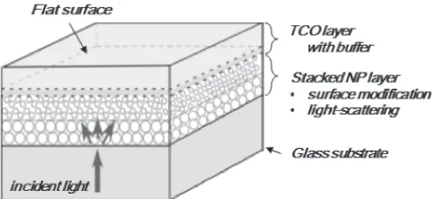
In this study, to improve the light-trapping capacity in Si thinfilms, without increasing the surface roughness of TCO substrates, we formed a stacked nanoparticle (NP) layer between the glass substrate and TCO layers, as shown in Fig. 1. The stacked TCO/NP/glass (NP-TCO) substrate was composed of three major parts, the large-sized NP layer (bottom), the small-sized NP layer (middle), and TCO layer
(top), which served as light-scattering, surface modification, and low-resistive layers, respectively. When light passes into the NP layer, it is scattered by the NPs. The light-scattering capacity of the NP layer is therefore determined by not only their surface roughness but also the light-scattering capacity of the NPs composing this layer. In addition, if the light-scattering capacity of within the NP layer is much higher than the surface roughness, obtaining a highly light-scattering substrate with a smooth surface morphology by surface modification is possible. Therefore, we formed NP-TCO substrates with a small-sized NP layer on light-scattering NP layers with different NP diameters, and examined their surface morphology, roughness, and light-scattering capacity.
2. Experimental Details
2.1 Fabrication method of NP-TCO substrates
The NP layers was first fabricated on the glass substrate (Eagle XG, Corning). In this study, to fabricate the light-scattering and surface modification layers of NP-TCO substrates, two types NP ZnO (NP-ZnO) and NP TiO2
(NP-TiO2) pastes were used. The ZnO paste was predominantly
prepared from approximately 30 nm sized (primary) nano-crystalline-ZnO (Sumitomo Osaka Cement Co., Ltd.) and 2-butanol, which served as the dispersion solvent. The ZnO
Fig. 1 Schematic of stacked TCO/nanoparticle/glass (NP-TCO) substrate for transparent electrode of thinfilm Si solar cells.
+Corresponding author, E-mail: r3815005@edu.gifu-u.ac.jp
[image:1.595.307.549.333.444.2]paste was mixed 33 mass% in 2-butanol (65 mass%), with a dispersant of acetylacetone (2 mass%), and sonicated at 350 W for 1 h to obtain colloidal solutions by an ultrasonic horn (Qsonica Q500, WAKEN B TECH Co., Ltd.). All NP-ZnO layers were coated by spin-coating method at 2000 rpm and then dried for 10 min at 70°C in air condition. In addition, to obtain different-sized NP-ZnO by necking-effects,20)NP-ZnO layers were heated for 1 h at temperatures of 450°C, 500°C, 550°C, 600°C, and 650°C in an electric furnace (HPM-OG, AS ONE Co.), respectively. After the formation of the light-scattering layer, the NP-TiO2layer was
fabricated onto NP-ZnO layers by the squeegee method. The NP-TiO2 paste (PST-18NR, JGC C&C Ltd.) was
predom-inantly prepared from approximately 18 nm sized (primary) anatase-type nanocrystalline-TiO2. Stacked NP layers were
then dried for 10 min at 70°C in air, after which they were heated for 1 h at 450°C in an electric furnace.
Al-doped zinc oxide (AZO) films were subsequently prepared on stacked NP layers as a low-resistivity layer using the radio frequency magnetron sputtering method, with a ceramicZnO : Al2O3(99 : 1mass%, 71 mm diameter)
target. During deposition, the distance between the AZO target and the substrate was maintained at 75 mm. The deposition chamber pressure was reduced to less than 7.0©10¹4Pa prior to the deposition using a rotary and turbo molecular pumps. The deposition power, pressure, and the substrate heating temperature were maintained at 150 W, 0.5 Pa, and 400°C, respectively. However, due to the high internal stress,21)the AZOfilm depositedfilms easily peeled
off from the underlying NP layer after few days. To improve the contact between the AZO and NP layers, we formed a 10 nm-thick low-stressed indium tin oxide (ITO; Sn-doped 10 mass%)film between the NP layers and the AZOfilm as a buffer layer,22)as shown in Fig. 1.
2.2 Measurement methods
Scanning electron microscopy (SEM; S-4800, HITACHI Ltd.) was used to examine the surface morphology and thickness of all layers. In addition, the particle diameter of the NP layers heated at different temperatures was estimated from those of surface SEM images. The root-mean-square (RMS) roughness of the NP layer and TCO film surface was measured by atomic force microscopy (AFM; SPA400, HITACHI Ltd.). The optical characterization of the NP layers and TCO films was performed by a dual-beam ultraviolet-visible spectrophotometer (V-670, JASCO Co.) equipped with an integrating sphere, in a 2502500 nm wavelength range. We measured the total transmittance (Ttot) and diffuse
transmittance (Tdiff) of all NP layers and TCO films. In this
study, the NP layers were composed of NPs and air. Thus, the refractive index of the NP layers (nNP) was lower than that of
the bulk layers (nbulk), and its value was determined by the
volume fraction (x) of NPs in the NP layer.23,24)We therefore calculated the refractive index of the NP layers from the optical interference between the single NP layer and the glass substrate in the low light-scattering wavelength rage of 1000 1500 nm using the equation as follows:
nNP ¼ 1
2dNP
12
12
ð1Þ
where,dNPis the thickness of the NP layer estimated from the
cross-sectional SEM image, and1and2are the wavelengths
of the adjacent maximum transmittance. The NP layer volume fractions were determined from the ratio of the refractive index of air (nairapproximately 1.0) and the bulk ZnO and
TiO2.25,26)We subsequently estimated the refractive index at a
wavelength of 600 nm using the equation as follows:
nNPðÞ ¼xnbulkðÞ þ ð1xÞnair ð2Þ
As a measure of the light-scattering capacity, the trans-mittance haze values for all samples were calculated by the equation as follows:
Haze value¼Tdiff
Ttot 100½% ð3Þ
The resistivity of the TCOfilms deposited on the NP layers was determined by the van der Pauw four-probe method.
3. Results and Discussions
3.1 Property of stacked NP-TCO substrate
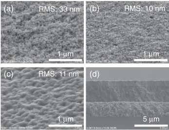
The NP layers and the stacked NP-TCO substrates had good transparency and were milky white in color owing to their strong light-scattering capacities. Figure 2(a)(c) shows surface SEM images of all layers of the stacked NP-TCO substrate. Images are labeled with the corresponding RMS roughness of their surface. In addition, a cross-sectional SEM image of the stacked NP-TCO substrate is shown in Fig. 2(d). In this figure, all NP layers were sintered at 450°C with layer thicknesses of approximately 1000 nm (AZO), 2400 nm (NP-TiO2), and 2000 nm (NP-ZnO). The
sheet resistance of the NP-TCO substrate was approximately 10³/sq. Based on the surface SEM images, the NP-ZnO layer had a rough surface morphology, with a relatively high RMS roughness of 32 nm, and was composed of relatively large NPs with a mean diameter of approximately 33 nm. After the coating of the NP-TiO2layer, the NP-ZnO layer was
covered by small-sized TiO2 particles (diameter:
approxi-mately 18 nm), and indicated relatively low RMS roughness of approximately 10 nm. After the deposition of the TCO films, as a consequence of the crystal growing of the AZO film, NP-TCO substrate had a small textured morphology with a grain size of approximately 100 nm, and a slightly increased RMS roughness of 11 nm. However, the observed RMS value is much lower than the light-scattering textured TCO films fabricated by alternate methods, and the TCO films directly deposited on the NP-ZnO layers (RMS: approximately 22 nm, not shown). This result indicates that a small particle intermediate layer is a useful surface modification for the NP-TCO substrate.
approx-imately 1.55 and 1.70, at a wavelength of 600 nm, with the corresponding volume fractions of these NP layers of approximately 0.55 and 0.5, respectively. These results indicate that a substantial amount of void space exists within the NP layers. After coating NP-TiO2on the NP-ZnO layer,
the transmittance of the stacked NP-TiO2/NP-ZnO layer decreased slightly, approximately 3%, in all wavelength ranges, as the NP-TiO2 layer had a higher refractive index
than the NP-ZnO layer. On the other hand, the light-scattering capacity of the stacked NP-TiO2/NP-ZnO layer was almost identical to the NP-ZnO layer, regardless of its low RMS value. This result indicates that the light-scattering capacity of the NP-ZnO layer was predominantly determined by the light-scattering capacity of the NPs within this layer. After
the TCO deposition, the NP-TCO substrate exhibited good transparency (approximately 80%) in the visible to near-infrared wavelength range, with a high light-scattering capacity. Moreover, the transmittance of the stacked NP-TCO substrate was slightly higher than that of the directly coated TCO/NP-ZnO substrate in the visible wavelength range. Thus, the NP-TiO2 layer works as an antireflective
layer in this substrate, as NP-TiO2 layer had an intermediate
refractive index between the NP-ZnO layer and the AZO thin film (n: approximately 1.9).
3.2 NP-TCO substrate with differing particle size light-scattering layers
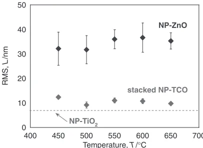
The light-scattering capacity of NPs is well known to be primarily determined by the particle diameter.27,28) Thus, to further improve the light-scattering capacity, we fabricated the NP-TCO substrates by the necking-effects, with different-sized underlying NP layers. Figure 4 shows surface SEM images of the underlying NP-ZnO layers sintered at varying temperatures, i.e., 450°C, 500°C, 550°C, 600°C, and 650°C, respectively. The initial NP-ZnO layer sintered at 450°C was composed of relatively small particles. However, the particle diameter of the NP-ZnO layers increased with an increase in their sintering temperature. Figure 5 shows the particle diameter of the NP-ZnO layers estimated from those of surface SEM images at different sintering temperatures. The particle diameter of the NP-ZnO layers increased with the sintering temperature. Consequently, the mean diameter of ZnO particles increased from approximately 33 nm (450°C) to 96 nm (650°C).
Figure 6 shows the RMS roughness of the NP-TCO substrates and those of underlying NP-ZnO sintered at different temperatures. In addition, the RMS roughness of the TCO films directly deposited on the NP-TiO2 layer
(a)
(b)
(c)
(d)
1
μ
m
1
μ
m
RMS: 33 nm
RMS: 10 nm
RMS: 11 nm
1
μ
m
5
μ
m
Fig. 2 Surface SEM images of (a) NP-ZnO layer sintered at 450°C, (b) stacked NP-TiO2/NP-ZnO layer, (c) stacked NP-TCO substrate,
and (d) cross-sectional SEM image of stacked NP-TCO substrate. The SEM images of (a)(c) were measured at tilted 60 degrees.
0 20 40 60 80 100
500 1000 1500 2000 2500
NP-ZnO NP-TiO
2/NP-ZnO TCO/NP-ZnO stacked NP-TCO
T
ransmittance [%]
Wavelength, λ/nm
Total
Diffuse
Fig. 3 The total transmittance (solid line) and diffuse transmittance (broken line) of NP-ZnO layer, staked NP-TiO2/NP-ZnO layer, TCO films
[image:3.595.124.471.69.336.2] [image:3.595.55.283.381.546.2](approximately 7 nm) is shown as a reference. The NP-ZnO layers had relatively high RMS roughness (approximately 30 nm), which gradually increased with increasing of ZnO particle diameter. However, the RMS roughness of the NP-ZnO layer sintered at elevated temperatures was compara-tively not high, regardless of the significantly increases in t particle size. We considered this a consequence of the composition of the NP-ZnO layers. The NP-ZnO layers sintered at high temperatures were composed of different-sized NPs, with their size dispersion also significantly increasing. Therefore, small particles in the NP-ZnO layers filled voids among the large ZnO particles, suppressing any increases in the surface roughness. This result clearly indicates that a small-sized NP effectively reduce the surface roughness of the NP layer. After the fabrication of the NP-TiO2 layer and TCO thin films, all NP-TCO substrates
exhibited homogeneous and smooth surface morphologies. Consequently, the RMS roughness significantly decreased to approximately 10 nm, regardless of the particle size compo-sition of the NP-ZnO layers. Furthermore, these RMS values were equivalent to the TCO films directly deposited on the NP-TiO2layer. This result indicates that the RMS roughness
of the NP-TCO substrates is predominantly determined by the roughness of the NP-TiO2 layer. This implies that
fabricating a NP-TCO substrate with lower RMS roughness using small-sized NP layer is possible.
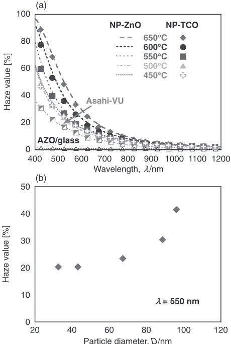
The haze value of the NP-TCO substrates composed by different-sized underlying NP-ZnO layers in the wavelength rage of 4001200 nm is shown in Fig. 7(a). In thisfigure, the symbol and the broken line indicate the haze value of the NP-TCO substrates and the underlying NP-ZnO layers, respec-tively, at differing sintering temperatures. In addition, the haze value of a widely used textured Asahi VU-type F-doped SnO2(Asahi-VU; ASAHI Glass Co., Ltd.) substrate is shown
as a reference. Due to its textured surface morphology (RMS: approximately 30 nm), the Asahi-VU substrate had a relatively high haze value of approximately 15% at 550 nm wavelength. On the other hand, the NP-TCO substrates indicated much higher light-scattering capacity than textured Asahi-VU in the visible wavelength, regardless of their relatively low RMS roughness. In addition, due to increases in the particle size of the underlying NP-ZnO layer, the haze value of the NP-TCO substrates significantly improved with the increase in the sintering temperature. Moreover, the haze value of the NP-TCO substrate highly corresponded with those of the underlying NP-ZnO layers. This result indicates that the light-scattering capacity of the NP-TCO substrate was predominantly determined by that of the underlying
NP-(a)
(b)
1
μ
m
(c)
1
μ
m
1
μ
m
(d)
(e)
1
μ
m
1
μ
m
Fig. 4 Surface SEM images of underlying NP-ZnO layers at a different sintering temperatures; (a) 450°C, (b) 500°C, (c) 550°C, (d) 600°C, and (e) 650°C.
0 50 100 150
400 450 500 550 600 650 700
Particle diameter
,
D
/nm
Temperature, T/°C
Fig. 5 Particle diameter of underlying NP-ZnO layers sintered at different sintering temperatures.
0 10 20 30 40 50
400 450 500 550 600 650 700
RMS,
L
/nm
Temperature, T/°C
stacked NP-TCO
NP-ZnO
NP-TiO2
[image:4.595.107.489.69.263.2] [image:4.595.324.527.303.451.2] [image:4.595.68.271.304.452.2]ZnO layers. Figure 7(b) shows the haze value of the NP-TCO substrates at a wavelength of 550 nm as a function of the mean particle diameter of the underlying NP-ZnO layer. A haze value of approximately 20%was obtained from the NP-TCO substrate with a 33 nm-sized NP-ZnO layer. The haze value of the NP-TCO substrates gradually increased with that of the underlying NP-ZnO layer particle diameter. Con-sequently, a NP-TCO substrate with a very high haze value of approximately 40% was obtained by using a 96 nm-sized underlying NP-ZnO layer, without increasing the surface roughness. This result suggests that the further improvement of the light-scattering capacity of the NP-TCO substrate could be obtained by using a larger sized (>96 nm) underlying NP-ZnO layer.
4. Conclusion
To improve the efficiency of thin film Si solar cells, we formed different-sized stacked NP layers between a glass substrate and low-resistivity TCO thin films as a light-scattering and a surface modification layer. In this study, the NP-ZnO and NP-TiO2 layers were used as light-scattering
and surface modification layers, respectively. After the TCO films deposition, the stacked NP-TCO substrates exhibited high light-scattering capacity with a low RMS roughness of approximately 10 nm. In addition, the haze value of the
NP-TCO substrates was predominantly determined by the particle size of the underlying NP-ZnO layer, which increas-ed from 20%(33 nm) to 40%(96 nm) without an increase in the surface roughness. These results indicate that incorporat-ing NP layers in the TCO substrate is a very effective method of improving the light-scattering capacity of TCO substrate without increasing the surface roughness.
Acknowledgement
The authors would like to thank Enago (www.enago.jp) for the English language review.
REFERENCES
1) W. Chu, J. Lin, T. Lin, Y. Tsai, C. Kuo, M. Chung, T. Hsieh, L. Liu, F. Juang and N. Chen:Opt. Commun.285(2012) 33253328.
2) M. Mizuhashi, Y. Gotoh and K. Adachi:Jpn. J. Appl. Phys.27(1988) 20532061.
3) Q. Huang, Y. Liu, S. Yang, Y. Zhao and X. Zhang:Sol. Energy Mater. Sol. Cells103(2012) 134139.
4) M. Zeman, O. Isabella, S. Solntsev and K. Jager:Sol. Cells119(2013) 94111.
5) J. Müller, B. Rech, J. Springer and M. Vanecek:Sol. Energy77(2004) 917930.
6) J. Springer, B. Rech, W. Reets, J. Muller and M. Vanecek:Sol. Energy Mater. Sol. Cells85(2005) 111.
7) K. Sato, Y. Gotoh, Y. Wakayama, Y. Hayashi, K. Adachi and H. Nishimura: Rep. Res. Lab. Asahi Glass Co., Ltd.42(1992) 129. 8) T. Matsui, M. Tsukiji, H. Saika, T. Toyama and H. Okamoto:J.
Non-Cryst. Solids299302(2002) 11521156.
9) T. Nakada, Y. Ohkubo and A. Kunioka:Jpn. J. Appl. Phys.30(1991) 33443348.
10) W. W. Wenas, A. Yamada, M. Konagai and K. Takahashi:Jpn. J. Appl. Phys.30(1991) L441L443.
11) W. W. Wenas, A. Yamada, M. Konagai and K. Takahashi:Jpn. J. Appl. Phys.33(1994) L283L285.
12) H. Zhu, J. Hupkes, E. Bunte, J. Owen and S. M. Huang:Sol. Energy Mater. Sol. Cells95(2011) 964968.
13) A. Hongsingthong, T. Krajangsang, I. A. Yunaz, S. Miyajima and M. Konagai:Appl. Phys. Express3(2010) 051102051104.
14) A. Hongsingthong, I. A. Yunaz, S. Miyajima and M. Konagai:Sol. Energy Mater. Sol. Cells95(2011) 171174.
15) M. Mizuhashi, Y. Gotoh and K. Adachi:Jpn. J. Appl. Phys.27(1988) 20532061.
16) H. Sai and M. Kondo:J. Appl. Phys.105(2009) 094511.
17) H. Sakai, T. Yoshida, T. Hama and Y. Ichikawa:Jpn. J. Appl. Phys.29
(1990) 630635.
18) H. B. T. Li, R. H. Franken, J. K. Rath and R. E. I. Schropp:Sol. Energy Mater. Sol. Cells93(2009) 338349.
19) M. Python, E. V. Sauvain, J. Bailat, D. Domine, L. Fesquet, A. Shah and C. Vallif:J. Non-Cryst. Solids354(2008) 22582262.
20) M. Hu, K. P. Giapis and D. Poulikakos:Appl. Phys. Lett.98(2011) 211904.
21) E. Ando and M. Miyazaki:Thin Solid Films392(2001) 289293.
22) S. Takayama, T. Sugawara, A. Tanaka and T. Himuro: J. Vac. Sci. Technol. A21(2003) 13511354.
23) K. C. Krogman, T. Druffel and M. K. Sunkara: Nanotechnology16
(2005) S338S343.
24) P. Tao, Y. Li, A. Rungta, A. Viswanath, J. Gao, B. C. Benicewicz, R. W. Siegel and L. S. Schadler:J. Mater. Chem.21(2011) 18623 18629.
25) M. Bass:Handbook of Optics, Vol. 2, (McGraw-Hill, 1994). 26) S. Tanemura, L. Miao, P. Jin, K. Kaneko, A. Terai and N. N. Gabain:
Appl. Surf. Sci.212213(2003) 654660.
27) C. F. Bohren and D. R. Huffman:Absorption and Scattering of Light by
Small Particles, (Wiley, New York, 1983).
28) A. J. Cox, A. J. DeWeerd and J. Linden:Am. J. Phys.70(2002) 620. (a)
(b) 0 20 40 60 80 100
650°C
600°C 550°C
500°C
450°C
Haze value [%]
Wavelength, λ/nm
NP-ZnO NP-TCO
AZO/glass
Asahi-VU
0 10 20 30 40 50
400 500 600 700 800 900 1000 1100 1200
20 40 60 80 100 120
Haze value [%]
Particle diameter, D/nm
λ = 550 nm
[image:5.595.54.284.71.413.2]