Microstructural Evolution of Sn-58Bi
/
Cu Joints through Minor Zn Alloying
Substrate during Electromigration
Fengjiang Wang
1,*, Luting Liu
1, Lili Zhou
1, Jiheng Wang
2, Mingfang Wu
1and Xiaojing Wang
1 1Key Laboratory of Advanced Welding Technology of Jiangsu Province, Jiangsu University of Science and Technology,Zhenjiang 212003, China
2School of Materials Science and Engineering, Jiangsu University of Science and Technology, Zhenjiang 212003, China
Minor Zn was alloyed into Cu substrate to improve the electromigration reliability of Sn-58Bi/Cu solder joints in this paper. Electromigration behavior of Sn-58Bi/Cu and Sn-58Bi/Cu-4.89Zn was studied with the current density of 1.0 × 10⁴ A/cm2 from the
micro-structural evolution on the surface morphologies and the interior interfacial structure. In case of the surface morphologies in Sn-58Bi joints, the existence of Zn in Cu substrate effectively postponed the formation of Sn hillocks of whiskers at the anode side and the depletions/voids at the cathode side. From the observation of interior interfacial structure, Cu-Zn substrate obviously depressed Bi segregation and the growth of Bi-rich layer at the anode interface. Because Zn atoms were migrated from the anode to the cathode while Bi atoms were migrated from the cathode to the anode during electromigration, Zn atoms would fill the vacancies left behind by the migration of Bi atoms. The electromigra-tion resistance of Sn-58Bi solder joints was correspondingly improved by Zn alloyed into Cu substrate. the calculated DZ* of Bi atoms in the
Cu and Cu-4.89Zn substrate is 3.69 × 10⁻¹¹ cm2/s and 1.76 × 10⁻¹¹ cm2/s, which also illustrates there exists a slower diffusion rate for Bi
at-oms in Sn-58Bi solder joint with Cu-Zn substrate. [doi:10.2320/matertrans.M2017162]
(Received May 22, 2017; Accepted August 3, 2017; Published September 15, 2017)
Keywords: tin-bismuth solder, electromigration, copper-zinc substrate, hillocks, bismuth segregation
1. Introduction
Due to the increasing environmental concerns, the use of Sn-Pb solder has been banned in electronic products since 2006 by international legislations, which has led to the ex-tensive studies on Pb-free solder materials1), including
Sn-Ag-Cu, Sn-Cu, Sn-Ag, Sn-Bi and Sn-Zn2–7), etc. Among
these potential alternatives, Sn-58Bi eutectic solder is re-cently getting much attention due to its lower melting tem-perature at 139 C, which can obviously reduce the thermal warpage on the components and boards during assembling. Sn-Bi solder joints also have excellent joint strength, low co-efficient of thermal expansion, good wettability, superior creep resistance, and improved yield and fracture strength2,8).
With the scaling down of dimensions on packaging com-ponents, the current density through the solder bumps will be expected to reach about 104 A/cm2. Under such a current density, the metallic atoms are migrated with the current flow. In Sn-Bi/Cu solder joint, phase separation in the solder and Bi segregation to the interface were always produced at the anode after electromigration9–11). The interfacial embrit-tlement induced by Bi segregation will deteriorate the reli-ability of solder joint12). Therefore, to improve the electro-migration reliability of Sn-58Bi solder joint, it is necessary to decrease the growth on Bi-rich layer at the anode. Many researchers have added the alloying elements into Sn-58Bi solder and found that the electromigration performances of
Sn-58Bi solder were improved. For example, Li et al.13)
found that adding tungsten nanoparticles into Sn-58Bi solder improved the electromigration resistance and joint strength. Hu et al.14) proposed the addition of Al
2O3 nanoparticles into Sn-58Bi solder reduced the mean thickness of Bi-rich layer at the anode. The addition of Ag nanoparticles was
also verified to decrease the formation of Bi-rich layer at the interface and increase the shear strength of Sn-58Bi solder joint after electromigration15). Additionally, with Sn-Ag-Cu solder as the diffusion barrier, the formation of Bi-rich layer at the anode in Sn-58Bi solder joint was also effectively depressed16).
Besides adding alloying elements into Sn-58Bi solder, al-loying Cu substrate provides another opportunity to improve the interfacial structure and joint strength of Sn-58Bi solder, which was rarely reported in the literatures. Zou et al.17) and our previous paper18) studied the interfacial structure and joint strength of Sn-58Bi solder on Cu-Zn, Cu-Al and Cu-Ag substrates during isothermal aging, and interestingly found that the intermetallic compounds (IMCs) growth and joint strength were obviously improved by these alloying substrates. Therefore, we further studied the effect of Zn containing Cu substrate on the electromigration behavior of Sn-58Bi solder joint in this paper. The interfacial Bi segre-gation and the growth of hillocks in Sn-58Bi solder joints on Cu-Zn metallization substrate were investigated and com-pared with Sn-58Bi solder joints on Cu substrate during electromigration.
2. Experimental Procedures
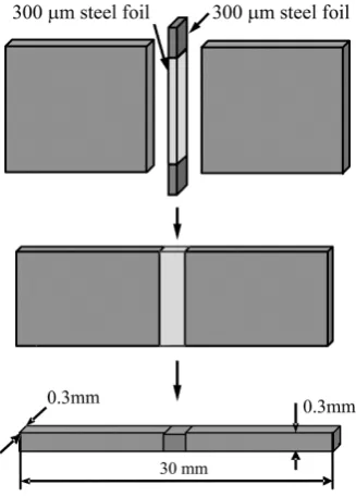
Oxygen-free Cu (OFC) and Cu-4.89Zn were used as the substrates. The fabrication of Cu-4.89Zn alloy was referred to our previous work18). They were finally supplied with the plates with size of 15 × 15 × 0.8 mm. Sn-58Bi solder was provided with the foils with the thickness of 300 μm.
The line-type joint was fabricated with schematic diagram shown in Fig. 1 and details illustrated in16). Unlike to the bumping structure, it provides a more uniform current den-sity distribute throughout the solder joint which reduces the impact from current crowding19). The reflowing temperature and time were 175 C and 30 s, respectively. After soldering,
* Corresponding author, E-mail: [email protected]
the joints were cut and polished to a thin bar with a cross-section of 0.3 mm × 0.3 mm and a length of 30 mm.
To have a direct observation on the surface morphology from the effect of electromigration on Sn-Bi joints, the sam-ples were mechanically and chemically polished to get a clean surface with a clearly observed microstructure.
Figure 2 shows an example on the cross-sectional Cu/
Sn-58Bi/Cu joint after soldering. The solder matrix is a typi-cally two-phase eutectic structure with white Bi-rich phases and grey Sn-rich phases. The electromigration was then per-formed with a calculated current density of 1.0 × 10⁴ A/cm2. Because joule heating from electromigration raised the tem-perature of solder joints, the samples were immersed into silicone oil during electromigration test, and a thermal cou-ple was attached around the samcou-ple to monitor the tempera-ture change. The temperatempera-ture of silicone oil increased by about 15 C during electromigration. The current stressing duration was selected as 33 h, 66 h, 99 h and 132 h, respec-tively. After tests, the polished surfaces were carefully cleaned with acetone and distilled water, and then observed with scanning electron microscopy (SEM) to get the effect of current stressing time on the surface morphology of sol-der joints. To observe the effect of electromigration on the interior interface of the solder joints, the current stressed samples were slightly polished and etched again. The inter-facial microstructure was analyzed by SEM and energy dis-persive X-ray (EDX).
[image:2.595.87.251.174.403.2]3. Results and discussion
Figure 3 shows the backscattered electron (BSE) images on the interfacial microstructure formed between Sn-58Bi solder and Cu or Cu-4.89Zn substrate after soldering at 175 C for 30 s. A thin IMC layer was observed at both
Sn-58Bi/Cu and Sn-58Bi/Cu-4.89Zn interfaces. The
composi-tion of IMC was Cu6Sn5 phase confirmed by EDX. It seems minor Zn in Cu substrate did not enroll in the reaction of Cu and Sn. However, Kim et al.20) and Yu et al.21) have pro-posed that Zn atoms could dissolve into Cu6Sn5 IMC phases by replacing some Sn atoms during the formation of Cu6Sn5 IMC layer. From the microstructural observation, alloying Zn into Cu substrate was slightly beneficial to the refinement of grain size in the Sn-58Bi solder matrix.
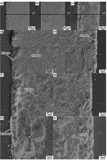
The surface morphology of Cu/Sn-58Bi/Cu solder joints under current density of 1.0 × 10⁴ A/cm2 was examined at intervals to trace the evolution of damage, and the results are shown in Fig. 4. It includes the effect of different stressing time on the cross-sectional joint, the anode interface and the cathode interface, respectively. The direction of electron flow is from the right to the left. Compared with Fig. 2, the surface morphology became rough after current stressing.
Fig. 2 SEM image on Sn-58Bi/Cu solder joint.
Fig. 3 Interfaces at (a) Sn-58Bi/Cu and (b) Sn-58Bi/Cu-4.89Zn as-soldered joints. Fig. 1 Sketch on solder joint fabrication.
[image:2.595.64.276.436.591.2] [image:2.595.98.498.621.771.2]After 33 h current stressing, the anode side shows a bulging morphology, as shown in Fig. 4(d), while the cathode side shows a dimpling morphology, as shown in Fig. 4(e). In the solder matrix, stress release patterns were observed along the grain boundaries close to the cathode side. After current stressing for 66 h, the step-shaped stress release patterns fully covered the joint, and more hillocks were squeezed out at the anode side, as shown in Fig. 4(f). With stressing time continued to 132 h, continuous extrusion of the hillocks at the anode side promoted the formation of whiskers shown in
Fig. 4(h). The rack of lines can be clearly observed at sur-face of the whiskers, which is usually believed to be the common feature of the whiskers. At the cathode side in Fig. 4(i), continuous current stressing finally promoted the formation of voids. In the cross-sectional solder joint shown in Fig. 4(c), the left area near the anode was higher than the right area near the cathode due to the compressive stress in the anode region and the tensile stress in the cathode region, which will be discussed later.
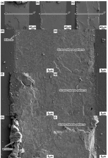
With 4.89 mass% Zn alloyed into Cu substrate, Fig. 5
[image:3.595.113.485.65.621.2]shows the corresponding surface morphologies after current stressing. After current stressing for 33 h, stress releasing patterns were clearly observed in the solder matrix but no obvious bulging or dimpling was occurred at the anode or cathode side compared with Cu substrate. With stressing time increased to 66 h, some discontinuous hillocks formed and solder bulged at the anode side, but others were rela-tively smooth. When the current stressing was applied to the solder joint for 132 h, whiskers were produced at the anode side, and the extrusion was occurred in the solder at the
cathode side. Meanwhile, boundary between the left bulging and the right dimpling was also easily observed in the cross-sectional solder joint.
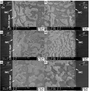
Because the growth of metal hillocks was from the bot-tom, it was necessary to investigate their interior microstruc-ture and its relationship with the stressing time. The samples with electromigration were polished and observed with SEM. Figures 6 and 7 show the interfacial structures in Sn-Bi/Cu and Sn-Bi/Cu-Zn joints after current stressing for 33 h, 66 h and 132 h, respectively. The left- and
right-col-Fig. 5 Surface morphologies of Sn-58Bi/Cu-Zn solder joints after current stressing for (a) 33 h, (b) 66 h and (c) 132 h in which the images on the left-, middle- and right-column represent the cross section, the anode side and the cathode side, respectively.
[image:4.595.111.487.67.616.2]umn also represent the anode side and cathode side, respec-tively. It can be observed that massive Bi atoms were accu-mulated at the anode side to promote Bi segregation and the formation of Bi-rich layer at the anode. With stressing time increasing, more Bi atoms migrated to the anode side to thicken the Bi-rich layer. Meanwhile, the thickness of IMC layer at anode side increased with the stressing time, while at cathode side, the dissolution of Cu substrate was occurred due to atomic migration from cathode to anode under elec-tromigration and there was no obvious increase on IMC thickness due to the polarity effect from electromigration22).
With Zn alloyed into Cu substrate, we can observe the ob-vious difference on growth thickness of Bi-rich layer and IMC thickness at the cathode side. Figure 8 shows the com-parisons on the growth of Bi-rich layer and IMC layer at an-ode side, in which the thickness was averaged by dividing the total area by the width of area. As observed from the variations in Fig. 8(a), the Bi-rich layer at the anode side grew almost linearly with the current stressing time, but its
thickness on Cu-Zn was far thinner than that in Sn-Bi/Cu
joint under the same duration of current stressing, which suggests that Zn alloyed into Cu substrate was beneficial to depress the growth of Bi-rich layer at the anode interface for Sn-Bi solder. The thickness of IMC layer at anode side was
also measured with the current stressing time. The IMC growth in solder joint usually follows the parabolic model during solid aging or solid current stressing, and follows the empirical diffusion formula:
X= √Dt+X0 (1)
where X is the total IMC thickness, X0 is the initial IMC thickness, t is the time and D is the diffusivity of IMC layer. Therefore, the IMC thickness was plotted with the square root of stressing time with the curve shown in Fig. 8(b), which really follows a linear regression between them. The
result shows that the IMC thickness in Sn-58Bi/Cu-Zn
sol-der joint was little higher than that in Sn-58Bi/Cu joint. The composition of IMC in Sn-Bi solder joints was Cu6Sn5, and its growth was mainly attributed to the reaction between Cu atoms diffused from the substrate and Sn atoms from the solder matrix. Correspondingly, thicker Bi-rich layer at the anode side in Sn-Bi/Cu solder joint inhibited the interdiffu-sion of Sn and Cu atoms, which lead to a relatively thinner IMC layer at the interface.
Electromigration is referred to the mass or atomic trans-port driven by the combination of thermal and electrical ef-fects. Under the electric current flow, the momentum trans-fer from electrons to atoms usually drives atoms from the
[image:5.595.113.484.68.448.2]cathode to the anode and vacancies from the anode to the cathode. With more solder atoms driven into the anode and vacancies into the cathode, a very high compressive stress
and tensile stress will be produced in the region at the anode and the cathode, respectively, which will result in the forma-tion of protrusion or hillocks at anode and depleforma-tion or voids
Fig. 8 The thickness of (a) Bi-rich layer and (b) IMC layer at the anode side with stressing time.
Fig. 7 Interfacial structures in the Cu-Zn/Sn-58Bi/Cu-Zn solder joints after electromigration for various durations: (a) and (b) 33 h, (c) and (d) 66 h, and (e) and (f) 132 h.
[image:6.595.113.483.67.488.2] [image:6.595.82.513.526.712.2]at cathode due to the stress releasing, as seen in Fig. 4 on Cu/Sn-58Bi/Cu joints and Fig. 5 on Cu-Zn/Sn-58Bi/Cu-Zn joints. At the anode side, the relationship between the exte-rior hillocks or whiskers and inteexte-rior Bi-rich layer must be considered. In Figs. 6 and 7, the formation of Bi-rich layer at the anode indicated that Bi atoms migrated with the elec-tron flow. The compressive stress formed at the anode side due to the excessive atomic accumulation when the Bi atoms migrated toward the anode side. On the contrary, tensile stress formed at the cathode side due to the atomic depar-ture. The compressive stress at the anode increased with the migration of Bi atoms into the anode region, and then finally released with the protrusion of hillocks or whiskers at the anode region. EDX confirms that the composition of whis-ker in Fig. 5(c) is 91.1 mass% Sn, 2.1 mass% Cu and 6.8 mass% Bi, which is a typical Sn whisker. The formation of Sn whisker at the anode area is helpful to release the com-pressive stress and also important to provide the crystal sites for the incoming Bi atoms during electromigraiton. On the other hand, due to the gradient on vacancy concentration, back stress will be produced between the tensile cathode re-gion and the compressive anode rere-gion, which retards the atomic transport during electromigration. Therefore, the atomic diffusion flux J occurred in electromigration can usu-ally be expressed by23):
J=Jem+Jσ=CD/kT(eZ∗ρj−Ω∂σ/σx) (2)
where Jem is the mass flux resulted from electron wind force,
Jσ is the mass flux resulted from back stress, C is the
con-centration of Bi in the Sn-Bi eutectic solder, k is Boltzmann constant, T is the absolute temperature, e is the electronic charge, Z * is the effective charge number, ρ is the electrical resistivity, j is the current density, Ω is the atomic volume, and ∂σ/σx is the stress gradient.
The formation of hillocks and whiskers at the anode inter-face and the formation of depletion or voids at the cathode interface are the common phenomena in Sn-solder with Cu or Cu-Zn substrate. However, what s the important things are the differences on the surface flatness and thickness of Bi-rich layer caused from Zn alloying Cu substrate. The relative flatter surface in solder matrix and thinner Bi-rich layer at anode interface represent that the rate of electromigration in the Sn-Bi/Cu-Zn joint is slower than that in the Sn-Bi/Cu joint. Ouyang et al.24) pointed out that the difference on sur-face flatness reflected the difference on local vacancy distri-bution in the solder joints during electromigration. In
Sn-58Bi/Cu solder joints, the apparent unevenness on surface
morphology illustrated that large amounts of lattice sites were depleted at the cathode side by vacancy absorption and created at the anode side by vacancy annihilation, respec-tively. Besides through the hillocks and whiskers at the an-ode interface and the depletion or voids at the cathan-ode inter-face, the stress release was also occurred through the protrusion of grains in the solder matrix. In Fig. 4, the pro-trusion of Sn grains almost covers the whole surface. Sn grains were considered to be favorable sites for stress releas-ing instead of Bi grains due to the difference on the crystal structure of Sn and Bi. The crystal structure of Sn and Bi be-longs to a body-centered tetragonal and rhombohedral struc-ture, respectively. The former structure shows an easier
plas-tic deformation during creep. Therefore, the back stress was reduced due to the adequate release under electromigration in the Sn-Bi/Cu solder joints. Accordingly, large amounts of Bi atoms were migrated into the anode region to promote a thicker Bi-rich layer at the anode interface. However, in Sn-58Bi/Cu-Zn solder joints, the relative flat surface means less absorption or annihilation of vacancies during electromigra-tion. Therefore, there existed a high back stress in the solder joints, and so the retardation on atomic migration from back stress increased. The possible reason may be attributed to the existence of Zn atoms. During soldering, Zn atoms from the Cu-Zn substrate was dissolved into interfacial Cu6Sn5 IMC and also diffused into the liquid Sn-58Bi solder matrix. During electromigration, the continuous growth of IMC layer at the anode interface and the dissolution of IMC layer at the cathode further released Zn atoms to the solder matrix. It is well known that the flow of Zn atoms was from the an-ode side to the cathan-ode side under a higher back stress25), which was opposite to the direction of Bi atoms. Because the migration of Zn atoms to the cathode side would fill the vacancies left behind by the migration of Bi atoms, it was helpful to slow the diffusion of Bi atoms to the anode and the formation of Bi-rich layer at the anode side.
This retarding effect can be estimated by the mass flux of
Bi atoms induced by electromigration. Chen et al.26)
pro-posed that the EM-induced atomic flux of Bi can be calcu-lated by:
Jem=vBi×d×(N/m)×57% (3)
Where vBi is the accumulation rate of Bi-rich layer, d is the density of Bi (9.8 g/cm3), N is the Avogadro s number (6.02 × 10²³ atoms/mol), and m is the atomic weight of Bi
(208.98 g/mol). The average accumulation rate of Bi-rich
layer in Sn-Bi/Cu and Sn-Bi/Cu-Zn is 4.65 × 10⁻⁵μm/s and 2.79 × 10⁻⁶μm/s, respectively. According to eq. (3), J
em can be calculated to be 1.31 × 10¹⁴ atoms/cm2·s and 7.88 × 10¹² atoms/cm2·s. From eq. (2), the product of the diffusiv-ity and the effective charge number DZ *, can be calculated as the following equation:
DZ∗=J
emkT/eρjc (4)
It should be mentioned that the real temperature on sam-ple measured by thermal cousam-ple was about 15 C higher than the room temperature due to the effect of Joule heating. Therefore, by substituting k = 1.38 × 10⁻²³ J/K, e = 1.6 × 10⁻¹⁹ C, ρ = 30 × 10−6Ω·cm, j = 1.0 × 10⁴ A/cm2, C = 1.41 × 10²² atoms/cm3, the DZ * in Sn-58Bi solder with the Cu and Cu-4.89Zn substrate is about 3.69 × 10⁻¹¹ cm2/s and 1.76 × 10⁻¹¹ cm2/s, respectively. Sn-58Bi solder with Cu-Zn shows a smaller DZ *.
4. Conclusion
In this study, the electromigration behavior of Sn-58Bi/
Cu and Sn-58Bi/Cu-4.89Zn solder joints was compared.
The microstructural evolutions on the surface morphology
and interior interfacial structure of Sn-58Bi/Cu and
Sn-58Bi/Cu-4.89Zn were investigated. The main conclusions
were as follows:
whiskers were protruded from the anode surface to re-lease the compressive stress while depletions were oc-curred from the cathode surface due to the existence of tensile stress, but Sn-58Bi/Cu-Zn solder joint substrate showed a higher resistance to electromigration.
(2) A continuous Bi-rich layer was produced at the anode interface due to Bi segregation diffused from the cathode side under electromigration. Its thickness linearly
in-creased with the stressing durations. Sn-58Bi/Cu-Zn
solder joint also showed a slower growth rate on Bi-rich layer.
(3) The higher retarding effect on electromigration from Cu-Zn substrate is attributed to the reason that Zn atoms in the Sn-Bi solder matrix diffused from Cu-Zn sub-strate plays an opposite migration compared with the moving direction of Bi atoms. The decrease on electro-migration-induced Bi atomic flux and the product of dif-fusivity and effective charge number (DZ *) of Bi veri-fied it. The calculated DZ * of Bi atoms in the Cu and
Cu-4.89Zn substrate is determined to be 3.69 ×
10−11 cm2/s and 1.76 × 10⁻¹¹ cm2/s, respectively.
Acknowledgement
This research is supported by projects funded by National Natural Science Foundation of China (Grant No. 51541104) and Jiangsu Planning Project of Science and Technology (Grant No. BK2012163, BK20150466).
REFERENCES
1) L. Zhang and K.N. Tu: Mater. Sci. Eng. Rep. 82 (2014) 1–32.
2) D. Ye, C. Du, M. Wu and Z. Lai: J. Mater. Sci. Mater. Electron. 26 (2015) 3629–3637.
3) T. Kadoguchi, K. Gotou, K. Yamanaka, S. Nagao and K. Suganuma:
Microelectron. Reliab. 55 (2015) 2554–2559.
4) M.-Y. Guo, C.K. Lin, C. Chen and K.N. Tu: Intermetallics 29 (2012) 155–158.
5) G. Ren, I.J. Wilding and M.N. Collins: J. Alloy. Compd. 665 (2016) 251–260.
6) X.J. Wang, N. Liu, S. Shi and Y.X. Chen: Adv. Mater. Sci. Eng. (2015) 257231.
7) J.X. Wang and H. Nishikawa: Microelectron. Reliab. 54 (2014) 1583–1591.
8) Z. Lai and D. Ye: J. Mater. Sci. Mater. Electron. 27 (2016) 3182–3192.
9) X. Gu and Y.C. Chan: J. Appl. Phys. 105 (2009) 093537.
10) J.H. Kim, Y.C. Lee, S.M. Lee and S.B. Jung: Microelectron. Eng. 120 (2014) 77–84.
11) Y. Liu, H. Fu, F. Sun, H. Zhang, X. Kong and T. Xin: J. Mater. Process. Technol. 238 (2016) 290–296.
12) Z. Lai, X. Kong and Q. You: J. Mater. Sci. Mater. Electron. 28 (2017) 4506–4512.
13) Y. Li, K.M. Luo, A.B.Y. Lim, Z. Chen, F.S. Wu and Y.C. Chan: Mater. Sci. Eng. A 669 (2016) 291–303.
14) T.W. Hu, Y. Li, Y.C. Chan and F.S. Wu: Microelectron. Reliab. 55 (2015) 1226–1233.
15) S. Ismathullakhan, H.Y. Lau and Y.C. Chan: Microsyst. Technol. 19 (2013) 1069–1080.
16) F. Wang, L. Zhou, Z. Zhang, J. Wang, X. Wang and M. Wu: J. Electron. Mater. (2017).
17) H.F. Zou, Q.K. Zhang and Z.F. Zhang: Mater. Sci. Eng. A 532 (2012) 167–177.
18) F.J. Wang, L.L. Zhou, X.J. Wang and P. He: J. Alloy. Compd. 688 (2016) 639–648.
19) H. He, G. Xu and F. Guo: J. Mater. Sci. 45 (2010) 334–340.
20) Y.M. Kim, T.J. Kim, M.Y. Choi and Y.-H. Kim: J. Alloy. Compd. 575 (2013) 350–358.
21) C.-Y. Yu and J.-G. Duh: Scr. Mater. 65 (2011) 783–786.
22) X. Gu, D. Yang, Y.C. Chan and B.Y. Wu: J. Mater. Res. 23 (2008) 2591–2596.
23) I.A. Blech and C. Herring: Appl. Phys. Lett. 29 (1976) 131–133.
24) F.-Y. Ouyang, K. Chen, K.N. Tu and Y.-S. Lai: Appl. Phys. Lett. 91 (2007) 231919.
25) X.F. Zhang, J.D. Guo and J.K. Shang: J. Mater. Res. 23 (2008) 3370–3378.
26) L.-T. Chen and C.-M. Chen: J. Mater. Res. 21 (2006) 962–969.