the sintering mechanism of the nanoparticles on the substrate. The simulation revealed that silver atoms from 1 and 2 nm nanoparticles migrated freely because of their larger surface energy and then epitaxially reoriented to the gold substrate so as to reduce grain boundary energy. The silver nanoparticles were more spread out on the (011) gold substrate than on the (001) substrate, indicating that substrates with larger surface energy induce greater spreading rates. Consideration of the competition of neck growth and epitaxial growth in sintering of nanoparticles revealed that reduction of surface energy is the predominant driving force in the initiation of sintering of silver nanoparticles, and that the reduction of grain boundary energy is subsequently consequential. [doi:10.2320/matertrans.MB201201]
(Received May 30, 2012; Accepted July 5, 2012; Published August 29, 2012)
Keywords: silver nanoparticle, molecular dynamics simulation, interfacial bonding, neck growth, epitaxial layer
1. Introduction
Electronic devices are required to not only work efficiently at elevated temperatures but also reduce power consumption when packaged. Bonding technology that can meet these requirements must be developed, and specifically needed are workable alternatives to lead-rich high melting point solders, which contain chemical substances that are hazardous to the environment. The difficulty in developing lead-free solders for use at high temperatures arises from the requirement that the metallic bonds between semiconductor chip mounted parts and various wiring connections exhibit long-term reliability. In particular, semiconductor chip mounted com-ponents (i.e., die-bonded parts) generate considerable heat and thus need improved thermal resistance, and the discharge characteristics of certain parts must be maintained to enable stable operation of the chips.1,2)
It is well known that particles smaller than 10 nm display different characteristics from those in the bulk state,36) including detectably lower melting points and sintering temperatures. This phenomenon originates from the large surface energy of the nanoparticles. If the activated nature of the nanoparticles significantly affects the surface atoms of the bulk metal, metal-to-metal bonding using nanoparticles as a
filler material can be achieved at significantly lower bonding temperatures than those in conventional fusion welding or diffusion bonding. This unique property of nanoparticles could be exploited in bonding materials in electronic devices in order to satisfy the conditions of improved thermal characteristics discussed above.
The application of nanoparticles as bonded materials for die-attach technology is widely anticipated, and there are numerous fruitful studies exploring low-temperature sintering nanoparticle pastes.711)Therefore, the dynamic study of the initial stage of sintering of nanoparticles on metal substrate is important to understanding basic experimental studies of the bonding process using nanoparticles. Industrially, gold coat-ings have long been used to protect conductor surfaces from
oxidation and to thereby promote their solderability.12) Accordingly, the study of the sintering behavior of silver nanoparticles on a gold-coated surface is highly relevant to the application of silver nanoparticles as a bonding material.
We have previously observed the silver/gold interface bonded at 523 K under a bonding pressure of 5 MPa using metallo-organic nanoparticles13) and identified that the sintered silver atoms were crystallographically oriented to the gold substrate, as shown in Fig. 1. This result indicates that the epitaxial layer of silver is formed in the bonding process. To understand the bonding mechanism precisely, it is necessary to study the initial stage of sintering of silver nanoparticles on a gold substrate. The dynamics of the sintering process cannot be observed with conventional experimental techniques, and therefore, computational inves-tigations were applied to this system.
We propose a novel bonding process using silver nano-particles2,1316) and in-situ formation of nanoparticles from silver oxide particles1,1719) that can serve as an alternative to the current micro soldering using a high-temperature solder, such as Pb10Sn or Pb5Sn. In the present study, the initial process of sintering of silver nanoparticles on a gold substrate was investigated using molecular dynamics (MD) simulation.
2. Simulation Method
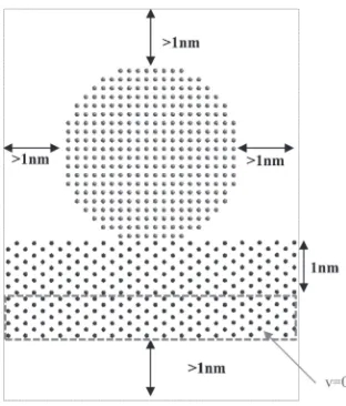
Molecular dynamics simulation was performed with conventional software (Materials Explorer 5.0 made by Fujitsu Ltd.). For a potential function, a generalized embedded atom method (GEAM) potential, which is included in the MD software, was applied.20)These potentials are wellfitted to basic materials properties.20)The simulated temperature was set to 523 K for comparison with our experimental result.13)The cross section of a typical model of a silver nanoparticle and a gold substrate is shown in Fig. 2. A silver nanoparticle with (001) orientation was set on (001) and (110) gold substrates without pressure, respectively, in order to evaluate the effect of misorientation between a silver
nanoparticle and a gold substrate on sintering behavior. The periodic boundary condition was set over a 1 nm distance from the nanoparticle in order to remove the interaction between nanoparticles. The velocity of atoms 1 nm below the surface in the substrate was set as 0. In order to estimate the sinterability of the nanoparticle, the neck size ratio, rs, was evaluated as follows:
rs¼
x
d ð1Þ
wherexis the neck length (contact length) during calculation and d is the initial diameter of a nanoparticle as shown in Fig. 3. The number of epitaxial layers on a gold substrate,
N, was also measured.
3. Results
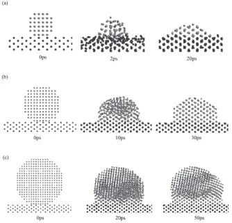
[image:2.595.68.530.70.187.2] [image:2.595.90.246.228.411.2]To evaluate the initial process of dynamic sintering of silver nanoparticles, MD simulation was applied to the sintering of a silver nanoparticle on the gold substrate. Figure 4 shows the atom arrangements of 1, 2 and 4 nm silver particles and a gold substrate with (001) orientation at 523 K. In 1 and 2 nm particles (Figs. 4(a) and 4(b)), silver atoms freely migrated at the beginning of the run, then re-crystallized and sintered on the gold substrate. The sintering process reached equilibrium within 20 ps. Conversely, for the 4 nm silver particle (Fig. 4(c)), atoms did not migrate freely but maintained the lattice organization. Necking also occurred within the silver nanoparticle. Epitaxial layers were clearly formed on the substrate for all silver nanoparticles during sintering. Moreover, it should be noted that there was no mutual diffusion of silver and gold atoms at the interface under any conditions tested.
Figure 5 shows the atom arrangement on the (011) gold substrate at 523 K. The effect of particle size on atom arrangement is very similar to what was observed for (001) substrates (Fig. 4); for the 4 nm nanoparticle, silver atoms were epitaxially arranged on the gold substrate below the neck. Moreover, at the silver/gold interface, the arrangement of silver atoms on the (011) substrate indicated better sinterability than those on the (001) substrate.
To evaluate the sinterability precisely, the neck size ratio was estimated for all silver nanoparticles. Figure 6 shows the neck size ratio as a function of sintering time in 1, 2 and 4 nm particles on the (a) (001) and (b) (011) substrates. In 1 nm particles on the (001) substrate (Fig. 6(a)), the neck size ratio rapidly increased at the beginning of sintering (3 ps) before reaching a nearly constant value at holding times longer than 10 ps. It was also found that, with increasing particle size, the growth rate and the saturation value of the neck size ratio both decreased. The values for the neck size ratio of nanoparticles on the (011) substrate (Fig. 6(b)) were larger as compared to those for the (001) substrate for all particle sizes, which indicates that the formation rate of the contacted area (interface) of the silver nanoparticle on the (011) substrate is larger than that on the (001) substrate.
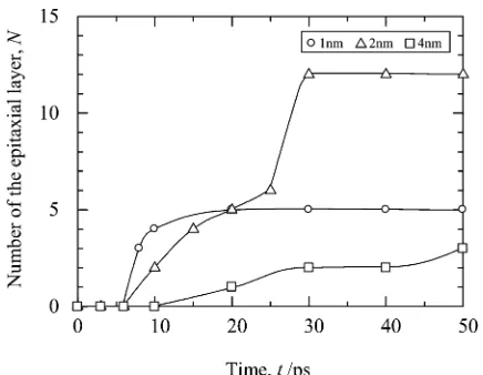
Figure 7 shows the number of epitaxial layers arranged on the (011) substrate during simulation. All atoms were epitaxially arranged on the substrate within 20 ps (1 nm nanoparticle) and 30 ps (2 nm nanoparticle), which means that the sintering of smaller nanoparticles on the substrate was completed within picoseconds. However, for 4 nm
/ fi fi
Fig. 2 Molecular dynamics model of a silver nanoparticle on a gold substrate.
[image:2.595.48.291.460.563.2]Fig. 4 Atom arrangements of (a) 1 nm, (b) 2 nm and (c) 4 nm silver particles on the gold substrate with (001) orientation at 523 K. Corresponding simulation times are also shown.
[image:3.595.131.462.75.380.2] [image:3.595.132.466.444.764.2]nanoparticles, the formation rate of the epitaxial layers was lower than that for 1 and 2 nm nanoparticles, and the arrangement was formed only below the neck.
To clarify the difference in the neck growth (interface formation) between (001) and (011) substrates, the tracks of migration of silver atoms during simulation were inves-tigated. The tracks of atoms in 4 nm nanoparticles on the (001) and (011) substrates are shown in Fig. 8. The black line shows the track of each surface atom at the cross section of the silver nanoparticle. It was found that surface atoms of a nanoparticle near the gold substrate were oriented to the substrate (1 and 2 in Figs. 8(a) and 8(b)). Once the atoms were oriented on the substrate, they did not migrate further. The surface atoms distant from the substrate (3 in Figs. 8(a) and 8(b)), on the other hand, migrated not to the substrate but onto the atoms which were epitaxially oriented on the substrate and did not affect interface formation and growth. As for the effect of the orientation of the substrate, it should be noted that the surface atoms near the interface migrated over a larger distance on the (011) substrate (1 in Fig. 8(b)) than on the (001) substrate (1 in Fig. 8(a)).
4. Discussion
Sintering is a non-equilibrium process in which surfaces and grain boundaries of the particle and substrate evolve toward an equilibrium so as to minimize the sum of the surface energy,£s, and the grain boundary energy,£gb. This is given as follows:
E¼£sAsþ£gbAgb ð2Þ
where,E,AsandAgbare the total free energy, the surface area, and the grain boundary area of a nanoparticle and a substrate, respectively. It is important to distinguish between the effects of neck growth and epitaxial growth on sintering because these behaviors result from changes in the surface energy and the grain boundary energy, respectively. The neck length ratio,rN, and epitaxial layer ratio,rE, divided by the saturated values up to the saturation of atom arrangement, are estimated as follows:
rN¼
rs
rs=saturated ð
3Þ
rE¼
N Nt=saturated
[image:4.595.86.512.69.243.2]ð4Þ
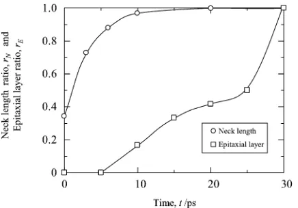
Figure 9 shows the relationship between the neck length ratio or epitaxial growth rate and the calculated saturation time for the 2 nm silver nanoparticle on the (011) substrate at 523 K. The saturation time is 30 ps, clearly indicating that neck growth occurs first and then subsequently the atoms epitaxially arrange on the substrate. Therefore, it appears that reduction of the surface energy is the predominant driving force in the initial sintering of silver nanoparticles (<10 ps), and after that, the reduction of the grain boundary energy occurs.
Concerning the sintering of nanoparticles to bulk metals, Yeadon et al.21) have reported that sputtered silver nano-particles formed an epitaxial layer on a monocrystal copper substrate under vacuum. They have also suggested that formation of the epitaxial layer begins within an extremely short time (picoseconds). The present work agrees well with their report, as we observed that for 1 and 2 nm nanoparticles, the atoms randomly migrated and epitaxially arranged on the
Fig. 6 Relationship between the neck size ratio and calculated time from MD simulation for each size of silver nanoparticle and the gold substrate with an orientation of (a) (001) and (b) (011) at 523 K.
[image:4.595.60.278.297.466.2]substrate on the order of picoseconds regardless of the orientation (Figs. 4 and 5). At the initial stage of sintering, simulation results also showed that silver atoms migrated freely. K. K. Nanda et al.22) have reported that the surface energy of free silver nanoparticles is 7.2 J/m2, which is higher than that of the bulk silver (1.35.9 J/m2). This suggests that the randomness in silver atom organization was likely the result of the melting of nanoparticles due to the large surface energy. Subsequently, silver atoms reoriented to the gold substrate and the epitaxial layer formed as a result of the reduction of the grain boundary energy, as the lattice constant of silver (0.4086 nm) is very close to that of gold (0.4079 nm).23)As the size of nanoparticles increased, melting did not occur and the neck size ratio decreased due to the lower surface energy, as was seen for the 4 nm nanoparticles in Fig. 6.
As for the effect of orientation on the substrate, the values of the neck size ratio on the (011) substrate are larger as compared to those on the (001) substrate for all particle sizes (Fig. 6(b)). This is easily explained by the higher surface energy of the (011) gold substrate (1.006 J/m2) as compared to that of the (001) gold substrate (0.894 J/m2),24) which caused the atoms near the (011) substrate to migrate more than those on the (001) substrate, as shown in the track of the silver atom in Fig. 8. In addition, the nanoparticles on the (011) substrate exhibited larger neck size ratios (Fig. 6). The
substrate with the larger surface energy promoted a larger spreading rate of the nanoparticles on the substrate. In the experimental process of metal-to-metal bonding using nano-particles, applied pressure and longer holding times than the present calculation time must accelerate the neck growth and epitaxial arrangement of the nanoparticles, which produces silver layers epitaxially oriented on the gold substrate as shown in Fig. 1.
5. Conclusions
The sintering behavior of a silver nanoparticle on a gold substrate was investigated using MD simulation in order to elucidate the sintering mechanism of the nanoparticle on the substrate. The MD simulation revealed that silver atoms in 1 and 2 nm nanoparticles freely migrated on the gold substrate. This randomness of silver atom organization is most likely caused by the melting of the nanoparticle due to the large surface energy. Subsequently, silver atoms reoriented to the gold substrate to reduce the grain boundary energy, and an epitaxial layer formed because the lattice constant of silver is very close to that of gold. It was also found that the silver nanoparticles on the (011) gold substrate were more highly wetted than those on the (001) substrate. This indicates that substrates with larger surface energy promoted a greater spreading rate of the nanoparticles on the substrate. The consideration of the competition of neck growth and epitaxial growth in sintering of nanoparticles revealed that reduction of the surface energy is the predominant driving force in the initial sintering of silver nanoparticles on the substrate, and that the reduction of the grain boundary energy subsequently plays a role in atom organization.
Acknowledgement
The computation was mainly carried out using the computer facilities at the Research Institute for Information Technology, Kyushu University. This work was supported by Grant-in-Aid for Scientific Research (B) No. 23360322, Japan, and by Priority Assistance for the Formation of Worldwide Renowned Centers of Research®The Global COE Program (Project: Center of Excellence for Advanced Structural and Functional Materials Design) from the Ministry of Education, Culture, Sports, Science and Tech-nology (MEXT), Japan.
Fig. 9 Relationships between the neck length ratio or epitaxial growth ratio and calculated time for a 2 nm silver nanoparticle and the (011) gold substrate at 523 K.
[image:5.595.103.494.70.203.2] [image:5.595.62.280.252.404.2]7) J. G. Bai and G. Q. Lu:IEEE Trans. Device Mater. Reliab.6(2006) 436441.
8) A. Hu, J. Y. Guo, H. Alarifi, G. Patane, Y. Zhou, G. Compagnini and C. X. Xu:Appl. Phys. Lett.97(2010) 153117.
9) Y. Morisada, T. Nagaoka, M. Fukusumi, Y. Kashiwagi, M. Yamamoto, M. Nakamoto, H. Kakiuchi and Y. Yoshida:J. Electron. Mater. 40
(2011) 23982402.
10) K. Suganuma, S. Sakamoto, N. Kagami, D. Wakuda, K. S. Kim and M. Nogi:Microelectron. Reliab.52(2012) 375380.
11) Y. Kobayashi, T. Shirochi, Y. Yasuda and T. Morita:Int. J. Adhes. Adhes.33(2012) 5055.
12) T. Laurila, V. Vuorinen and M. Paulasto-Kröckel:Mater. Sci. Eng. R68
19) A. Hirose, N. Takeda, Y. Konaka, H. Tatsumi, Y. Akada, T. Ogura, E. Ide and T. Morita:Mater. Sci. Forum706709(2012) 29622967.
20) X. W. Zhou, R. A. Johnson and H. N. G. Wadley:Phys. Rev. B69
(2004) 144113.
21) M. Yeadon, J. C. Yang, R. S. Averback, J. W. Bullard and J. M. Gibson:
Nanostruct. Mater.10(1998) 731739.
22) K. K. Nanda, A. Maisels, F. E. Kruis, H. Fissan and S. Stappert:Phys. Rev. Lett.91(2003) 106102.
23) Japan Institute of Metals (ed.):Metals data book, (Maruzen, Tokyo, 2004) p. 36.