Development of PVD coating processes informed by
plasma diagnostics.
EHIASARIAN, Arutiun Papken.
Available from Sheffield Hallam University Research Archive (SHURA) at:
http://shura.shu.ac.uk/19603/
This document is the author deposited version. You are advised to consult the publisher's version if you wish to cite from it.
Published version
EHIASARIAN, Arutiun Papken. (2002). Development of PVD coating processes informed by plasma diagnostics. Doctoral, Sheffield Hallam University (United Kingdom)..
Copyright and re-use policy
See http://shura.shu.ac.uk/information.html
REFERENCE
ProQuest Number: 10694484
All rights reserved INFORMATION TO ALL USERS
The quality of this reproduction is dependent upon the quality of the copy submitted. In the unlikely event that the author did not send a com plete manuscript and there are missing pages, these will be noted. Also, if material had to be removed,
a note will indicate the deletion.
uest
ProQuest 10694484
Published by ProQuest LLC(2017). Copyright of the Dissertation is held by the Author.
All rights reserved.
This work is protected against unauthorized copying under Title 17, United States C ode Microform Edition © ProQuest LLC.
ProQuest LLC.
789 East Eisenhower Parkway P.O. Box 1346
Development of PVD Coating Processes
Informed by Plasma Diagnostics
Arutiun Papken Ehiasarian
A thesis submitted in partial fulfilment of the requirements of
Sheffield Hallam University
for the degree of
Doctor of Philosophy
h a lla m
UJipbrf
huijhpflLl, UJl if 111Jl [l h PuipqbGJiB
Abstract
Physical vapour deposition technologies have been on the fast track of development for the last two decades due to their ability to meet demands for special materials and performance tools. The ever increasing complexity of the required coating microstructure and chemical composition can be achieved only by the development of PVD technology and in particular plasma sources for vapour generation that can provide the necessary tools.
This thesis describes plasma diagnostic studies of plasma discharges, developments of plasma sources and deposition of CrN coatings.
Initially the project investigated vacuum arc plasma discharges used in the Hauzer HTC1000/ABS industrially sized coater. The attention was concentrated to the plasma pretreatment by low energy (1200 - 3600 eV) Cr ion implantation into substrates, which contributed to an enhanced adhesion of subsequently deposited TiAIN coatings. Optical emission spectroscopy (OES), electrostatic probes, and time-of-flight (TOF) spectroscopy were used to study the interactions of the arc plasma with the gas atmosphere in the chamber. It was shown that increasing the pressure of Ar gas had a strong effect on the composition of the generated metal ion flux as the density of highly charged metal species reduced significantly to the benefit of gas ionisation. The mechanisms behind these observations are discussed and supported by further experiments. Based on the plasma diagnostic results, a novel two-stage pretreatment method was developed which allowed an enhanced adhesion due to faster sputter cleaning of the substrate surface and more efficient metal ion incorporation in the substrate material.
In the final stages of the project a novel high power pulsed magnetron sputtering (HIPIMS) process utilising peak power densities of 3000 W on'2 was investigated. OES studies showed the first evidence of doubly charged Cr and Ti ions generated by the HIPIMS discharge. Peak plasma densities of 1013 cm'3 were measured and, in the case of Cr, metal ions were found to constitute 30% of the total deposition flux to substrates. The influence of power on the plasma density, plasma composition and time evolution of the plasma was studied in detail using OES and electrostatic probes. The conditions for glow-to-arc transition were investigated. CrN coatings (thickness 2pm) were deposited for the first time using HIPIMS of Cr in a nitrogen atmosphere. The microstructure observed in transmission electron microscopy cross sections was highly dense and droplet free and contributed to an excellent corrosion and wear resistance superior to 20 pm thick electroplated hard Cr, and CrN coatings deposited by arc and unbalanced magnetron sputtering. The HIPIMS discharge was used also for pretreatment of substrates with metal ions analogous to the one performed previously with arc discharge. High adhesion was achieved as indicated by the scratch test critical load value Lc = 85 N.
Acknowledgements
I would like to thank Dr. Roger New, my Director of Studies, for giving me invaluable guidance to conduct scientifically sound experiments and for his patience and support during my growth as a scientist. I would like to thank also Prof. W.-D. Miinz, my First Supervisor, for sharing with me his invaluable experience in building industrially viable products based on state of the art fundamental scientific research.
The work constituting the present thesis benefited immensely from a number of visiting collaborations with leading laboratories in the field of plasma and materials research worldwide. In large part these visits were possible thanks to the remarkable capabilities of Prof. W.-D. Miinz to network with leading scientists working in all aspects of PVD. The start of the PhD project was boosted during a visit to the HVM Plasma Ltd., Prague, Czech Republic, company where the expertise, experience, and professionalism of the people make state of the art development of plasma sources and PVD coatings based on plasma diagnostics, magnetic field modelling and material characterisation look like a child's play. In particular, I would like to acknowledge the great help of Dr. Jan Valter and Dr. Jiri Vyskocil.
At a more mature stage of the PhD project, a visit to the Materia Nova Research Centre in Mons, Belgium, was organised in order to study the radio frequency amplified magnetron sputtering process. The high level of commitment of the scientists (of whom only two physicists!) and a good taste for carnivals are models for anyone interested in optical emission spectroscopy and particle interactions in plasmas. I would like to thank Professor Michel Hecq, the director of the centre and my collaborators Dr. Corinne Nouvelon, Ms. Laettitia Blott and Mr. Stephanos Konstantinidis.
Towards the end of the PhD thesis, I visited the Thin Film Physics group at the University of Linkoping. The laboratory is famous for developing the superlattice coating structure and pioneering the studies of plasma-surface interactions in thin films. I would like to thank prof. Ulf Helmersson and prof. Lars Hultman who gave me the opportunity to test my abilities to apply and to extend my knowledge by working with the state of the art high power pulsed magnetron sputtering (HIPIMS) process. This unique technology has a great potential in the PVD field.
Finally, at the very end of the PhD project, I had the opportunity to work with Prof. Jochen Schneider of Aachen University and Dr. Andre Anders at the Lawrence Berkeley National Laboratory, Berkeley, U.S.A. This laboratory is one of the leaders worldwide in the analysis and modelling of arc discharge plasmas and plasma-surface interactions. The Plasma Applications group is famous for compiling a periodic table listing experimentally obtained and theoretically modelled charge state distributions of ion fluxes generated in arc discharges. I would like to thank Jochen for arranging the visit and for very fruitful discussions on science and scientific life. I would like to thank Andre for being a great scientific mentor and a good host.
Last but not least, I would like to acknowledge the scientific, technical and moral support of the entire Surface Engineering Research Group.
Advanced Studies
The following conferences, workshops and summer schools were attended during the studies for this thesis:
1. Fifth Sheffield ABS Days, July 1999, Sheffield, UK
2. 1st Plasma Technology Training School, June 2000, Buxton, UK 3. Sixth Sheffield ABS Days, July 2000, Sheffield, UK
4. Materials Week 2000, International Congress on Advanced Materials, their Processes and Applications, September 2000, Miinchen, Germany
5. Surface Engineering for Protection of Metals and Alloys, October 2000, Aquafreda di Maratea, Italy
6. 44 Annual Technical Conference of the Society of Vacuum Coaters (SVC), April 2001, Philadelphia, U.S.A.
7. International Conference on Metallurgical Coatings and Thin Films (ICMCTF) 2001, April 2002, San Diego, U.S.A.
8. 13 International Colloquium on Plasma Processes, June 2001, Antibes - Juan-les- Pins, France
9. Seventh Sheffield ABS Days, July 2001, Sheffield, UK
xL
10. 12 International School on Vacuum Electron Ion Technologies (VEIT), September 2001, Varna, Bulgaria
11. 48th International Symposium of the American Vacuum Society (AVS), November 2001, San Francisco, U.S.A.
12. Materials Congress 2002, April 2002, London, U.K.
tVi •
13. 45 Annual Technical Conference of the Society of Vacuum Coaters, April 2002, Orlando, U.S.A.
t h •
14. 5 Pulsed Plasma Surface Technologies Workshop and Tutorials, April 2002, Indialantic, U.S.A.
15. International Conference on Metallurgical Coatings and Thin Films 2002, April 2002, San Diego, U.S.A..
Publications and Patents
1. C. Schonjahn; A.P. Ehiasarian; D.B. Lewis; R. New; W.-D. Miinz; R.D. Twesten; I. Petrov, Optimisation of in situ Substrate Surface Treatment in a Cathodic Arc Plasma: A Study by TEM and Plasma Diagnostics, J Vac Sci Technol, A19(4), (2001),1415
2. A.P. Ehiasarian, W.-D. Munz, L. Hultman, U. Helmersson, V. Kouznetsov, Influence of High Power Densities on the Composition of Pulsed Magnetron Plasmas, Vacuum, 65, (2002), 147
3. K.M. Macak, A. Ehiasarian, W.D. Munz, Z. Khan, U. Helmersson, An Analysis of Breakdown Mechanisms of High Power Pulsed Magnetron Sputtering, Proceedings o f 13th International Colloquium on Plasma Processes, Antibes - Juan-les Pins, France, 2001
4. A.P. Ehiasarian, W.-D. Munz, L. Hultman, U. Helmersson, I. Petrov, High Power Pulsed Magnetron Sputtered CrNx Films, paper presented at ICMCTF 2002, San Diego, USA, accepted for publication in Surf Coat. Technol
5. J. Alami, J.T. Gudmundsson, A.P. Ehiasarian, W.-D. Miinz, U. Helmersson, Plasma Conditions in Ionized PVD by High-power Pulsed Magnetron Discharges, paper presented at ICMCTF 2002, San Diego, U.S.A.
6. W.-D. Miinz, D.B. Lewis, P.E. Hovsepian, C. Schonjahn, A. Ehiasarian, I.J. Smith, Industrial Scale Manufactured Superlattice Hard PVD Coatings, Surface
Engineering, 17(1), 15, 2001
7. G. Nayal, A.P. Ehiasarian, K.M. Macak. R. New, W.-D. Miinz, Low Pressure plasma nitriding, paper presented at eMRS, Strasbourg, (2000)
Awards
Bunshah Award. Symposium B, International Conference on Metallurgical Coatings and Thin Films, 2002, San Diego, U.S.A.
Table of Contents
Abstract iii
Acknowledgements iv
Advanced Studies v
Publications and Patents vi
Awards vii
Table* of Contents x
List of Figures and Tables xiii
1. Introduction 1-1
2. Literature Review 2-1
2.1. Plasma-Surface Interactions During Film Growth 2-1
2.1.1. Thin Film Microstructure Models 2-1
2.1.2. Ion to Neutral Ratio and Energy o f Ion Bombardment 2-5 2.1.3. Ions Impinging at a Substrate at High Energy (eg. > 1000 eV)2-8
2.2. PVD Plasma Sources 2-9
2.2.1. Cathodic Arc Evaporation 2-10
2.2.2. Magnetron Sputtering 2-15
2.2.3. Magnetron Sputtering with Auxiliary Electron Impact Ionisation 2-19
2.2.4. RF Coil Enhanced Magnetron Sputtering 2-20
2.2.5. High Power Pulsed Magnetron Sputtering 2-22
2.3. Chromium Nitride 2-25
Materials and Methods 3-1
3.1. Hauzer HTC 1000/ABS Coating Machine 3-2
3.2. Metal Vapour Vacuum Arc (M EW A) with Time-of-Flight Spectrometer
3-6
3.3. High Power Pulsed Magnetron Sputtering (HIPIMS) 3-10
3.4. RF Coil Enhanced Magnetron Sputtering (Universite de Mons-Hainaut,
Belgium) 3-13
3.5. Plasma Diagnostic Techniques 3-16
3.5.1. Optical Emission from Plasmas 3-16
3.5.2. Instruments Used for Optical Emission Spectroscopy 3-19 3.5.3. Flat and Cylindrical Electrostatic (Langmuir) Probes 3-21 3.5.4. Instruments Used for Electrostatic Probe Diagnostics 3-26
3.5.5. Energy Resolved Mass Spectroscopy 3-31
3.6. Thin Film Characterisation Methods 3-34
3.6.2. Etching Rate Measurement 3-34
3.6.3. X-Ray Diffraction (XRD) Analysis 3-34
' 3.6.4. Transmission Electron Microscopy (TEM) for Thin Film
Microstructure 3-36
3.6.5. Scanning TEM (EDX) 3-37
3.6.6. Evaluation o f the Adhesion o f Thin Films 3-38 3.6.7. Measurement o f the Hardness o f Thin Films 3-38 3.6.8. Measurements o f the Friction and Wear Coefficient in Sliding
Wear 3-39
4.1. Steered Cathodic Arc Discharge 4.1-1
4.1.1. Multi-fold Ionisation Observed In Cr, Ti, and Nb Metal Arc Discharges 4.1-1
4.1.2. Influence o f Gas Pressure on Plasma Density, and Electron Temperature
o f Cr Arc Discharge 4.1 -5
4.1.3. Development o f a Two-Stage Cathodic Arc Etching Procedure for
Enhanced Adhesion on HSS. 4.1-9
4.1.3.1. Ion Saturation Current o f Cr Arc Discharge in Ar Atmosphere 4.1-9 4.1.3.2. Plasma Composition o f Cr, Ti and Nb Arc Discharges in Kr,
Ar, Ne, and He Atmosphere 4.1-12
4.1.3.3. Coating Sequence Incorporating a Two-Step Etching
Treatment 4.1-26
4.1.3.4. Implantation Profiles o f Cr Ions at Different Ar Pressures 4.1-28
Summary 4.1-33
4.2. High Power Density Pulsed Magnetron Sputtering
(HIPIMS) Discharge 4.2-1
4.2.1. Influence o f High Power Densities on the I-U Characteristic o f
Magnetrons 4.2-3
4.2.2. Multi-Fold Ionised Metal Species Found in Cr, Ti, and Ta HIPIMS and
Comparison to Conventional Magnetron Discharge 4.2-6
4.2.3. Influence o f Peak Power on the Plasma Composition, Ion Density and
Deposition Rate 4.2-11
4.2.4. Time Evolution o f the Plasma Composition and Density During a Pulse
in HIPIMS o f Cr, Ta and C Targets 4.2-13
4.2.5. An analysis o f breakdown mechanisms o f high power pulsed magnetron
sputtering. 4.2-17
4.3. Deposition of CrN Films by Selected PVD Techniques 4.3-1
4.3.1. CrNfilms deposited by Reactive Unbalanced Magnetron
Sputtering 4.3-1
4.3.2. CrN films deposited by Reactive High Power Pulsed Magnetron
Sputtering (HIPIMS) 4.3-7
Summary 4.3-25
4.4. Unbalanced Magnetron Sputtering Glow Discharge with Enhanced Ionisation by Radio Frequency (RF) Coil
4.4-1
4.4.1. Typical Plasma Composition and Ion Energy in the RF Coil Amplified
Magnetron Discharge 4.4-2
4.4.2. Influence o f Power Dissipated in the RF Coil on Ion Density and Energy 4.4-5 4.4.3. Influence o f Ar pressure on the RF Coil Discharge 4.4-10 4.4.4. Implementation o f the RF Powered Coil in the Hauzer HTC1000/ABS™
Coating Deposition Machine and Influence o f RF Power and Pressure on
the Ionisation and Plasma Composition 4.4-12
5. Conclusions 5-1
6. References 6-1
Annex A. Engineering Drawing of the Mirror and Collimator
Assembly A-1
List of Figures and Tables
Figure 2.1. Zone model proposed by Movchan and Demchishin. For metals Ti = 0.3 Tm; T2 = 0.45 Tm
Figure 2.2. Thornton zone model
Figure 2.3. Messier model of PVD film microstructure
Figure 2.4. Structure zone model relating to closed field UBM sputtering configuration after Kelly and Amell [7].
Figure 2.5. Computer simulations of film growth under varying ion-to-neutral ratio in the deposition flux.
Figure 2.6. Refractive index versus C>2+ ion current density of alumina films produced
at T < 150°C after Williams et al [41]
Figure 2.7. Refractive index versus deposition rate at different target power settings taken from Shih and Dove [44].
Figure 2.8. The classification of plasma discharges according to their current density [52]
Figure 2.9. Basic arc evaporation processes and potential distribution after Martin et al [55]
Figure 2.10. Schematic of the deposition of a droplet and the structure of the film established in its vicinity after Petrov et al. [13]
Figure 2.11. Magnetic field arrangement in a steered cathodic arc discharge. 18 - evaporated cathode. 84 - magnets, 82 - magnetically conducting soft iron core. Adapted from Ramalingam [64]
Figure 2.12. Schematics of a planar magnetron illustrating the arrangement of magnets, the electric field and the plasma (shaded region)
Figure 2.13. Magnetic field lines of (a) balanced and (b) unbalanced circular magnetrons. The false colour represents the strength of the field.
Figure 2.14. RF coil enhanced magnetron sputtering set up, after Schneider et al [82] Figure 2.15. Time evolution of the target voltage, ion saturation current density, argon neutral emission intensity, and Ti neutral emission intensity. Figure adapted from Macak et al [98]
Figure 3.1. Horizontal cross section through the middle of the ABS machine
Figure 3.2. Magnetic flux density, B, at the target surface of Cathode 3 in Steered Arc (0 A coil current) and Magnetron (0 A coil current) configuration, (a) Normal
component of B, (b) tangential component of B.
Figure 3.3. Vertical cross-section of the vacuum chamber showing the Langmuir probe position and the probe and sampling volume for OES. The inset shows detailed view of the mirror assembly.
Figure 3.6. Oscillograms showing the arc current, the pulse driving the gates (Gate pulse), and charge/mass ratio dependent ion current trace (Time-of-Flight Spectrum), 500 ns/div.
Figure 3.7. Calculated relationship between the pressure measured in the TOF chamber and the actual pressure in the MEVVA source.
Figure 3.8. Schematic of the HIPIMS experimental setup
Figure 3.9. Top view of the laboratory sized RF coil enhanced magnetron sputtering setup.
Figure 3.10. Schematic diagram of the magnetron, RF coil, optical and energy resolved mass spectrometers
Figure 3.11. An example optical emission spectrum of Ti.
Figure 3.12. Monochromator with Czemy-Tumer geometry [120]
Figure 3.13. Blazed grating. Light is incident at angle a and diffracted at several orders -
Po, Pi
and p_i.Figure 3.14. Schematic of the optical emission spectroscopy experimental setup schematic
Figure 3.15. Sheath formation at a surface of an electrode (probe) Figure 3.16. Ideal flat probe characteristic
Figure 3.17. Sheath (collecting area) of flat (a) and cylindrical (b) electrostatic probes. The sheath is indicated with a wireframe with sheath width ds and the physical probe body is represented with a solid fill.
Figure 3.18. (a) Flat (plane) electrostatic probe and (b) Cylindrical probe used in the experiments
Figure 3.19. Electrical circuit used to record probe characteristics
Figure 3.20. Cylindrical probe I-V characteristic in a Cr arc discharge at background pressure (3x1 O'6 mbar), discharge current 100 A and cathode-to-probe distance of 20 cm. Oscillations in the probe current are caused by the motion of the cathode spot steered around the cathode surface.
Figure 3.21. Semilogarithmic I-V plot of a cylindrical probe obtained in a unbalanced magnetron discharge. Pure Ar atmosphere, 1.4x10'3 mbar, unbalancing coil current 6 A, discharge power 5 kW, cathode-to-probe distance of 20 cm.
Figure 3.22. Detail from Figure 3.21 showing the transition region of the I-V
characteristic used to determine the electron temperature. Two slopes corresponding to thermalised (cold) and fast diffusing (hot) electrons are evident.
Figure 3.23. Energy resolved mass spectrometer (Balzers PPM421) Figure 3.24. Geometry of the GA-XRD measurement.
Figure 3.25. Schematic of a TEM [138]
Figure 3.26. Loading/unloading curve of the dynamic hardness measurement Figure 3.27. Schematic of the pin-on-disk tester
Figure 4.1.2. Time of Flight spectrum for a Nb arc operated in a Kr atmosphere
Figure 4.1.3. High-speed photographs of a Cr arc discharge showing the different plasma conditions on the target due to adding background gas. (a) - Arc discharge operated at base pressure of 0.003 Pa, (b) Arc discharge operated in Ar gas
atmosphere at 0.1 Pa. Exposure time 1 ms. The composition of the post plasma is an estimate based on the dominating colour of the emission (red for Ar neutrals and blue for Cr ions and neutrals and Ar ions)
Figure 4.1.4. Ion saturation current densities measured by flat Langmuir probe for positions 0 = 0° (circles) and 0 = 90° (x) and cylindrical probe (rhombi and squares)
Figure 4.1.5. Etching rate of stainless steel substrates as a function of Ar pressure.
Figure 4.1.6. Variation of the emission from Cr neutrals, and ions with pressure. In Ar atmosphere (a) the emission is altered due to collisions with Ar atoms, in He
atmosphere (b) collisions are less effective.
Figure 4.1.7. Variation of the emission from Ti and Nb neutrals, and ions with pressure. In Ar atmosphere (a) the emission from Ti is altered due to collisions with Ar atoms, in He atmosphere (b) collisions with Ti ions are less effective. Nb neutral emission increases at higher Ar pressures than Ti and Cr (c).
Figure 4.1.8. Influence of gas pressure on highly charged ion densities. Legend the ions are represented by colour: Nb3+ - blue, Nb4+ - pink, Nb5+ - green, Cr2+ - orange, Cr4+ - light blue. The different gases forming the atmosphere are represented by symbols: Ne atmosphere - circles, Ar atmosphere - triangles, Kr atmosphere - squares.
Figure 4.1.9. Influence of gas pressure on low charged ion populations. Legend: the ions are represented by colour: Nb1+ - blue, Nb2+ - red, and Cr + - green. The different gases forming the atmosphere are represented by symbols: Ne - circles, Ar - triangles, Kr - squares.
I
Figure 4.1.10. Cr ion concentration as a function of gas pressure for three types of gases. The charge transfer between Cr2+ and Ne needs additional 5.07 eV.
Figure 4.1.11. Influence of gas pressure on the gas ion concentration in a Cr arc discharge.
Figure 4.1.12. Average charge state determined by Time of Flight Spectrometry of Cr and Nb random arcs as a function of pressure and type of atmosphere.
Figure 4.1.13. Process sequence of one step (standard) and two-step etching procedures.
Figure 4.1.14. Plan view dark field images of TiAIN coating grown on low carbon steel after (a) lOmin two step sputter cleaning procedure (b) 10 min sputter cleaning
Figure 4.1.15. STEM-EDX profiles across low carbon steel/TiAIN interfaces obtained by (a) mixed Cr/Ar ion bombardment at pAr = 6* 10'2 Pa for 10 min (b) mixed Cr/Ar ion bombardment at pAr = 8.8* 10'2 Pa followed by pure Cr ion bombardment.
Figure 4.2.1. Voltage and current density of plasma discharges. [52]
Figure 4.2.3. Ion saturation current at a distance of 35 mm with the probe facing the target (circles) and with the probe perpendicular to the target surface (squares). The flat probe was biased to -150 V. Maximum plasma densities derived from the current densities are in the range 1013 cm'3.
Figure 4.2.4. Optical Emission Spectra of HIPIMS of (a) Cr, (b) Ti, (c) Ta, and (d) C. Figure 4.2.5. Optical emission spectra of plasmas produced by discharges in a
conventional DC magnetron (bottom), a RF coil enhanced magnetron (middle) and High Power Pulsed Magnetron (top).
Figure 4.2.6. Carbon sputtering in N2 atmosphere - HIPIMS and Continuous
Figure 4.2.7. Ion to neutral ratio vs. peak target current for Cr from optical emission line intensities I( Cr2+ ) / 1( Cr° ) (triangles) and I( Cr1+ ) / 1( Cr° ) (circles). Also shown is the ratio of the ion current density and deposition rate (squares).
Figure 4.2.8. Typical time evolution of the optical emission and target current at low power (peak target voltage = -500 V)
Figure 4.2.9. Typical time evolution of the plasma at high power. Time resolved optical emission spectrum of HIPIMS of Ta at peak power density = 2 kWcm'2 Figure 4.2.10. Typical time evolution of the plasma at high power. HIPIMS of Cr at peak power density = 3 kWcm'2. The species shown are: Cr (399 nm), Cr1+ (232 nm), Ar° (811 nm), Ar1+ (440 nm). Js is the ion current
Figure 4.2.11. Typical time evolution of the plasma: target voltage and current at high power (the apparent fluctuations in the current signal after 80 ps are principally caused by digitisation noise).
Figure 4.2.12. Time dependence of arcing frequency
Figure 4.2.13. Arcing frequency dependence on energy per pulse (effective pulse power).
Figure 4.3.1. Influence of nitrogen flow, Qn2, on the partial pressures of Ar, Par , and
N2, Pn2, and the total pressure, Ptot. The resulting partial pressure ratios Pai-:Pn2 are
shown as labels on the Pn2 trace. It was attempted to keep the total pressure constant.
Figure 4.3.2. (a) Electron Temperature, Te; and (b) Plasma density at the substrate position for different Qn2/(Qat + Qn2) flow ratios.
Figure 4.3.3. XRD trace from CrN films deposited in the Hauzer ABS machine with Ubias = -300 V in mixed Ar+N2 gas atmosphere with the indicated partial pressure
ratios.
Figure 4.3.4. Deposition sequence
Figure 4.3.5. XTEM micrograph of the coating-substrate produced by HIPIMS. The line indicates the position and length of the area analysed by STEM-EDS
Figure 4.3.6. Chemical composition of the coating to substrate interface produced by HIPIMS. Data obtained by STEM-EDS point analysis. Ni signal is omitted.
Figure 4.3.7. Scratch test scar of CrN deposited on HSS.
out by QCM are marked with open circles. The full square represents a step height measurement.
Figure 4.3.9. Micrographs of CrN coating surfaces: (a) optical micrograph of CrN deposited by ABS technology (b) optical micrograph of CrN deposited by HIPIMS, (c) SEM micrograph of CrN deposited by ABS technology and (d) SEM micrograph of CrN deposited by HIPIMS
Figure 4.3.10. SEM micrograph of a CrN coating deposited by HIPIMS on 304 austenitic stainless steel.
Figure 4.3.11. The CrN coating surface viewed by (a) AFM (b) SEM. The coating conforms well to the structure of the steel grains.
Figure 4.3.12. TEM cross section of a CrN film produced by HIPIMS CrN. The films is columnar and the columns are terminated with flat tops.
Figure 4.3.13. XTEM micrograph showing the overall structure of HIPIMS CrN. Figure 4.3.14. XTEM micrographs of a HIPIMS CrN film, (a) Void free grain
boundaries (b) Grains are formed and extinguished far from the initial nucleation at the interface, (c) Strain and dislocation contrast is observed in the TEM image.
Figure 4.15. Plasma sheath near a floating substrate.
Figure 4.3.16. Glancing angle XRD scans (10° incidence) showing the phase
composition of HIPIMS CrN films deposited at different Ar:N2 partial pressure ratios.
Peaks of the C^N phase are marked in italics.
Figure 4.3.17. Bragg-Brentano XRD scans showing the microstructure of CrN films deposited at different Nitrogen partial pressures by Reactive HIPIMS.
Figure 4.3.18. Comparison of the sliding wear coefficient, K, of HIPIMS CrN to various coatings [170].
Figure 4.3.19. Potentiodynamic polarisation curve of monolithic CrN deposited by the HIPIMS method. The behaviour of electroplated hard Cr and arc deposited CrN is shown for comparison.
Figure 4.4.1. Typical OES spectra of an inductively coupled RF amplified magnetron discharge and conventional sputtering discharge. Ti ion lines are shaded. Conventional sputtering discharge with DC power = 200 W at Ar pressure 30 mTorr. RF coil
discharge in the same conditions and RF power = 500 W.
Figure 4.4.2. Typical mass spectrum of an inductively coupled RF amplified magnetron discharge. RF power 250 W, DC power 200 W, Ar pressure 30 mTorr. The small peaks on the sides of the Ti+ are from naturally occurring isotopes of Ti. Figure 4.4.3. Typical ion energy distribution function of Ar and Ti ions in an
inductively coupled RF amplified magnetron discharge conditions as in Figure 4.4.2 - RF power 250 W, DC power 200 W, Ar pressure 30 mTorr.
Figure 4.4.4. Magnetron target current increases with increasing RF coil power. Figure 4.4.5. Magnetron target voltage decreases with increasing RF coil power Figure 4.4.6. Optical emission signals as a function of RF Coil Power. 100 W DC, 10 mTorr.
Figure 4.4.8. Ion Energy Distribution for Ar Ions at Varying RF Coil Power at DC power 100 W, and Ar pressure of 10 mTorr
Figure 4.4.9. Dependence of the ion energy distribution function on the Ar pressure. Figure 4.4.10. Ion energy distribution function of Ar+ measured when the RF coil operated as a sole plasma generator
Figure 4.4.11. Overall appearance of the water cooled RF coil and feedthrough installed in the Hauzer HTC 1000/ABS™ coating machine
Figure 4.4.12. Water cooled 2-pin power feedthrough with coaxial connector and one half of the screening aluminium box.
Figure 4.4.13. Lower insulated support of the RF coil in the chamber.
Figure 4.4.14. Comparison of the Optical Emission of RF coil enhanced and conventional magnetron sputtering
Figure 4.4.15. Ion saturation current density as a function of applied RF power. Figure 4.4.16. Comparison of the ion saturation current density in RF enhanced and conventional magnetron sputtering
Figure 4.4.17. Ion saturation current density as a function of Ar gas pressure. RF power = 500 W
Table 4.1.1. Charge state distributions measured in the MEVVA random arc source for different cathode materials. The states marked in italics could be observed by the present OES setup.
Table 4.1.2 Plasma properties and ion flux at a distance of 25 cm from the source. Table 4.1.3. Ionisation potentials and energy defect after charge exchange
Table 4.1.4. Initial kinetic energy (eV) required to compensate for the energy deficiency in a charge exchange reaction
Table 4.2.1. Properties of selected HIPIMS target materials
Table 4.3.1 Mechanical properties of a CrN film deposited by the ABS technology at a Ar:N2 partial pressure ratio PAr:Pm — 1:1
1. Introduction
Background
The development of coating systems based on physical vapour deposition (PVD) processes has enjoyed a boost in the last 20 years with the introduction of ceramic protective coatings such as oxides and nitrides of the transition elements. These thin films have been implemented in a broad range of applications in the machining, automotive, textile, petrochemical, decorative, etc. industries with a total turnover of billions of pounds. The success of thin coatings is due to the wide range of properties, such as high hardness, low friction coefficients, and resistance to wear, corrosion, oxidation, and a variety of colours that are possible to achieve by variations in the chemical composition and microstructure. Evolution of new coatings has been strongly related to developments in the understanding of, specifically, plasma assisted PVD processes, and the improvement of PVD technology and high vacuum technology in general.
For example, the invention of the magnetron sputtering deposition technique enabled complex metallic (TiAl, TiAlY [1]) and even ceramic (AI2O3) systems to be vaporised in a reactive gas (N2, O2, ...) atmosphere and the production of, e.g. the third
generation nitride - TiAlCrYN [2] - with exceptional performance in metal cutting operations.
Studies of ion assisted film growth showed the dramatic influence of the ion energy and the ion-to-neutral ratio in the deposition flux on the microstructure of thin films. The control over these parameters has been enabled by further process development and the introduction of the unbalanced magnetron (UBM) [3]. UBMs use a magnetic field with a complex shape which simultaneously confines the plasma near the target surface, in order to increase the sputtering rates, and creates a magnetic path along which the dense plasma can flow out and reach long distances from the target, where the substrates are located.
The combination of different magnetron target materials enabled the commercialisation of high hardness nanoscale multilayered coatings with a ‘superlattice’ structure, consisting of different layers of ceramics in a common atomic lattice e.g. CrN/NbN, TiAlN/VN, etc. [176].
The superlattice columnar coating structure has a number of advantages in comparison to single layer columnar coatings. For example, the number of voids is decreased, healing of large scale growth defects is faster, and the wear mechanism are more favourable. The forced growth of the two different nanolayers constituting the superlattice structure into an atomic lattice, which does not match exactly either of the two, causes a high residual stress to be developed. The advantage of the high stress is that the superior properties of the superlattice coatings are combined with a high hardness [8], which can exceed the hardness of the constituent layers.
However, the adhesion to the substrate of superlattice coatings whose residual stresses can reach as much as 16 GPa is a critical issue. An elegant way of improving the adhesion to steel substrates is to promote localised epitaxial growth of the nitride films. The enhancement of the overall adhesion of the coatings to substrates influences strongly the performance in metal cutting applications for example [9], [10]. Localised epitaxy has been achieved by modifying the coating deposition process to include a pre treatment stage during which the substrates are irradiated with a highly energetic (> 1 keV) flux of metal ions that penetrates the steel to a short range and induces lattice deformation and recrystallisation of the material. For steel grains with specific orientation the deformation helps to achieve matching between the lattice of the substrate and the nitride. Subsequently deposited nitride film can grow epitaxially on these grains thus potentially increasing the adhesion to the extremely high levels of the ionic bond.
sputtering of metallic targets, typically in N2 atmosphere. The unique design of the
ABS cathodes allows the magnetic field to be adjusted so that the same cathodes can be used during both the pretreatment and the coating deposition stages. Furthermore, operating as many as four magnetrons simultaneously and moving the substrates so that they collect a deposition flux from the different cathodes allows the deposition of nanoscale multilayer coatings.
In a successful ABS deposition process, it is crucial to produce highly charged metal ions during the pre-treatment stage and increase the ion-to-neutral ratio during the deposition stage. As outlined above the first stage contributes to an enhanced adhesion. The second stage allows a greater flexibility in the choice of deposition materials as well as the benefit of surfaces with low roughness.
A distinct drawback of the ABS technique is the deposition of macroparticles of size in the range of a few hundred nanometres created during the arc discharge phase. The size of the macroparticles (ranging from 100-5000 nm [11]) is very large compared to the typical surface roughness of the substrates, and contributes to greatly enhanced shadowing effects during subsequent film growth and the development of macroscopic defects exceeding the size of the seed by an order of magnitude [12] reaching several micrometres above the substrate [13]. These growth defects are known to compromise the wear [14], oxidation [15] and corrosion [16] resistant properties of the coatings in metal cutting applications.
The removal of macroparticles from arc discharges is typically performed by curved magnetic duct or electrostatic Venetian blind' filters that separate neutral particles from the ion flux [67, 68]. However, the efficiency of these processes rarely exceeds 25% and new methods producing ionised metal at high rates are of strong interest to both the research and commercial community.
Present Work
high power (im)pulsed magnetron sputtering (HIPIMS) technique as a PVD method suitable for substrate pretreatment as well as coating deposition.
The investigations presented in this thesis are based on the equipment available to the Surface Engineering Research Group at Sheffield Hallam University incorporating the ABS process on an industrial scale in a commercially available Hauzer HTC 1000/ABS coating machine. This is equipped with four rectangular cathodes (600x200 mm) that can be operated in steered arc or closed field UBM mode simply by automatic modification of the magnetic field [6].
The PhD project was initiated with studies of the arc discharge plasma, which led to the development of an improved etching stage. It is shown that the new etching procedure derived from the plasma diagnostic results improves the adhesion of coatings to the substrate by increasing the etching/cleaning rates and enhancing the metal ion implantation profile [17].
The first attempt to produce a source with a high density of ionised metal vapour was based on magnetron sputtering with additional ionisation by a radio frequency powered coil. This approach was investigated in laboratory conditions and a working scaled up model was designed, manufactured, installed and tested in the industrially sized Hauzer HTC 1000/ABS coater.
The second attempt investigated the HIPIMS technique developed in 1995 by Mozgrin et al. [27] and Kouznetsov et al [21], [22]. The plasma composition produced in HIPIMS was characterised in detail for the first time [23], [24]. The investigations in this thesis present evidence of highly charged metal ions for the first time in these discharges [23]. The potential of the HIPIMS technique to influence the interface and improve the adhesion between hard coatings and metallic substrates has been demonstrated for the first time in this thesis. Potential commercial applications of this pretreatment method have been described in a patent application [25]. Finally, the first hard CrN coatings deposited by HIPIMS were produced and analysed, showing a superb corrosion and wear resistant behaviour [26]. The plasma characterisation and the hard coating investigations have shown the potential of the HIPIMS method as a new and powerful PVD tool.
interpret information. Chapter 4 contains the results from the relevant experiments and gives information necessary for the validation of the thesis. Finally, Chapter 5 contains the more important conclusions from the present work as well as an indication of some of the interesting problems requiring future investigations. A list of all references can be found in Chapter 6.
The experimental results and discussions are separated in four sections of Chapter 4 as follows.
Chapter 4.1 describes the development of a novel pre-treatment stage [17] whereby the incorporation of Cr metal ions into steel substrates is maximised and the adhesion of coatings improved. Plasma diagnostic studies of arc discharges in the presence of gas have indicated several important interactions that occur between metal ions and gas atoms that are characteristic of the process. High gas pressures lead to an increased scattering of metal ions. At the same time, gas atoms are ionised more readily thus increasing the ion flux to the substrates and contributing to a more efficient etching process. However, the number of highly charged metal ions can decrease significantly due to charge exchange collisions with gas atoms [18], whereby an electron is transferred from the neutral particle to the ion. Plasma diagnostic studies led to the realisation that splitting the pretreatment phase into stages with different operating conditions could make optimal use of the plasma conditions described above. The novel etching treatment combined a fast etching pre-treatment at high gas pressures followed by a pure metal ion bombardment at low gas pressure. The new etching technique is now being employed in commercial coating deposition runs.
The investigations presented in Chapters 4.2 and 4.3 describe the novel HIPIMS plasma source [21, 27].
Chapter 4.2 is dedicated to the study of plasma conditions in HIPIMS. This plasma source operates at typical peak-power-densities of 3000 Wcm'2 (two orders of magnitude higher than conventional UBM sputtering) dissipated in pulses with duration 100 ps. Plasma diagnostic characterisation of the discharge showed a high plasma density and the presence of up to 2-fold ionised metal ions for Cr and Ti. The time evolution of different species during the pulse duration showed a separation in time between gas and metal ions [23]. The conditions of glow-to-arc transition as a function of time and target power are discussed in detail [24].
UBM sputtering is a widely researched material [28], which is known to have a peak Knoop hardness of approximately HK0.025 = 2200. In this thesis it was attempted to
increase the hardness to values of HK0.025 = 3000 of CrN films by increasing the lattice
strains induced during the growth. A high-energy ion bombardment was used and, in order to compensate for the preferential sputtering of N2, high nitrogen partial pressure
was used [29, 30]. CrN films were deposited by HIPIMS for the first time. The microstructure observed in transmission electron microscopy cross sections was columnar and highly dense. The wear and corrosion resistance as well as the adhesion of the coatings was excellent. [26]
Chapter 4.4 of this thesis is dedicated to the diagnostics and industrial upscaling of a high ionisation density plasma source based on an inductively coupled radio frequency (RF) discharge [19]. The plasma source consisted of an unbalanced magnetron and a RF-powered concentric antenna that induced ionisation-enhancing currents in the plasma. The operation is analogous to a transformer in which the RF coil acts as the primary winding, and the plasma as the secondary winding [20]. Plasma diagnostic techniques were used to characterise the discharge parameters, plasma composition and ion energies in a laboratory-sized set up. An industrially sized RF coil was designed, constructed, and installed in the Hauzer ABS coater. Plasma diagnostic results showed that highly excited plasma with elevated density could be produced.
2. Literature Review
2.1. Plasma-Surface Interactions During
Film Growth
Since the discovery of sputtering by Sir William R. Grove in 1852 [31], physical vapour deposition (PVD) and thin films have found a remarkable range of applications. PVD methods, and in particular those enhanced by plasmas, are among the most versatile, economical and environmentally friendly. The diversity of thin film hardness, wear behaviour, electrical and thermal conductivity, colour, transparency, etc. that can be obtained by PVD methods is extraordinary. This diversity is largely possible because the microstructure, density, grain size, surface morphology, and chemical composition can be varied almost without bounds by varying the deposition temperature, the properties of the plasma and the nature of the interactions of the plasma with the growing film. Historically, the effect of substrate temperature was discovered first, revealing that, depending on the adatom mobility, PVD grown films can exhibit a range of microstructures. In further developments, extensive literature has been published establishing two properties of the deposition flux in plasma assisted (PAPVD) processes, which are crucial in determining the film micro structure:
a) Energy of ion bombardment b) Ion to neutral ratio
2.1.1. Thin Film Microstructure Models
The microstructure of thin films deposited by PVD methods is usually columnar. The density and size of columns depends strongly on the energy, mass, flux and angle of incidence of the bombarding particles. Also of importance is the absorption and deposition of particles with thermal energy such as reactive gases and metal atoms on the surface.
The zone 2 structure (0.3 < Ts/Tm < 0.5) had columnar grains defined by metallurgical grain boundaries formed under conditions of surface diffusion. Finally the zone 3 microstructure consisted of equiaxed grains recrystalised grains affected strongly by bulk diffusion.
Zone 1 Zone 2 Zone 3
[image:29.613.179.377.112.238.2]Temperature
Figure 2.1. Zone model proposed by Movchan and Demchishin [32]. For metals Tj = 0.3 Tm; T2 = 0.45 Tm
Thornton modified this model for the sputter deposition of coatings [33], taking into account the higher energy of sputtered atoms (5-25 eV as opposed to evaporation with 0.1 eV), and the possible loss of energy due to scattering in the gas phase. The zones defined by the model are determined not only by the temperature but also the total gas pressure which is an important parameter affecting the sputtering processes as well as the transport of particles from the sputtered target to the substrates. The same zones were observed as by Movchan and Demchishin, however a new transition zone T was found occurring between zone 1 and 2. Zone T is characterised with poorly defined densely packed fibrous grains. Figure 2.2 shows Zone 1, Zone T, Zone 2 and Zone 3 structures.
TRANSITION STRUCTURE CONSISTING OF
DENSELY PACKED FIBROUS GRAINS
COLUMNAR GRAINS
POROUS STRUCTURE CONSISTING OF TAPERED CRYSTA LITES SEPF. RATED BY VOIDS RECRYSTALIZED GRAIN STRUCTURE 26 ARGON PRESSURE (in TORR) ..z.
i ’•
ONI
ZONE T
ifiVIM i
*03
‘ 0 ,8
•0.7
0.6
*0,2 *03
OS
0 4 SUBSTRATE
[image:30.612.80.475.257.540.2]TEM PERATIJRE (T/Tm)
Figure 2.2. Thornton zone model
smooth transition microtructure Zone T can be produced at decreased homologous temperatures when ion bombardment with suitable energy is used.
100 0.8
[image:31.614.103.490.74.318.2]0.7
Figure 2.3. Messier model o f PVD film microstructure
The increase in bombardment energy however has an additional influence on film properties. For example high bias voltages lead to generation of lattice defects in the growing film. For TiN films a critical bias of -80 V has been found where the defect density observed in TEM cross sections is considerable [39]. As a result of these interactions the residual stress in the films can increase significantly up to values of -10 GPa. High energy Ar gas ions have been found to get trapped in the growing films and form gas bubbles due to irradiation enhanced diffusion. Recoil implantation of metal adatoms due to high energy gas ion bombardment can lead to intermixing, especially important in superlattice nanometre-size layer structures.
the homologous temperature Ts/Tm, the bias voltage on the substrates and the ion to neutral ratio Ji/Jn. Figure 2.4 shows a schematic of the closed field unbalanced magnetron sputtering model.
ZOh£3
[image:32.614.122.345.111.399.2]t
rrj
Figure 2.4. Structure zone model relating to closed field UBM sputtering configuration after Kelly and Arnell [7J.
2.1.2. Ion to Neutral Ratio and Energy of Ion Bombardment
Muller [37] employed molecular dynamics calculations for the simulation of the effect of ion bombardment during growth. In the model, Ni is thermally evaporated (energy bn the order of 0.03 eV) (see Figure 2.5) and bombarded with 50 eV Ar ions at an angle of incidence of a = 30°. Ion to neutral flux ratios Ji/Jn of (b) Ji/Jn = 0.04 and (c) Ji/Jn = 0.16 were modelled. The computer simulation shows that the packing density of the film is strongly related to the energy per deposited atom. The packing density increased towards bulk values with increasing ion energy Ei and/or ion-to- neutral vapour flux ratio Ji/Jn. For example, in low-Ts growth simulations, the films in the Monte Carlo simulations had porous structures in the absence of ion bombardment, whereas if ion irradiation effects were taken into account, quite different growth morphologies were obtained. The film density was observed to increase almost linearly with Ji/Jn. The calculations also predicted that there should be an optimum ion energy Ei* for densification. The optimisation resulted from the fact that for Ei>Ei* an increasing fraction of the ion energy is lost deeper in the lattice leaving vacancies which cannot be filled by arriving vapour species.
vapour
vapour
[image:33.614.196.365.349.636.2]vapour
At elevated Ts, low-energy ion irradiation can also reduce residual defect densities in epitaxial films [38]. Direct evidence of this is given by Petrov et al [39] and Hultman et al [40] for N2+ ion bombardment on growing TiN(lOO) films.
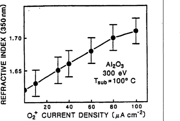
Experimental evidence for Mullers modelling results in general and for the densification of alumina films in particular is given by Williams et al [41]. The film packing density is related to the refractive index and was increased from 80% to 92% by increasing the flux of C>2+ ions at 300 eV from 0 to 100 pAcm"2, as can be seen in Figure
2.6. The density was correlated to the measured refractive index by Maxwell-Gamett [42], based on the assumption the film density is reduced by air or oxygen inclusions.
in
X 1.70
= 1.65
LL
100
80
40 60
20
[image:34.613.163.473.235.444.2]0 2+ CURRENT DENSITY C/iA cm '2}
Figure 2.6. Refractive index versus O2 ion current density o f alumina films produced
at T < 150°C after Williams et al [41]
500W
c
UJ o o:
u.
Ui
RATE OF DEPOSITION R (nm/mm)
Figure 2.7. Refractive index versus deposition rate at different target power settings taken from Shih and Dove [44].
2.1.3. Ions Impinging at a Substrate at High Energy (eg. > 1000 eV)
When ions bombard a substrate with energy exceeding three times the bonding energy of the substrate material sputtering can occur. For bombardment energies of approximately 5 keV the sputtering yield of most materials reaches saturation [45], which is attributed to a balance between sputtering and implantation. The depth of implantation depends on the energy as well as the dose of ions. Hubler et al [46] have shown that the actual projected range of nitrogen ions into iron increases linearly with ion energy. The actual implantation profile however is also influenced by the ion dose. Computer simulations [46] have shown that as the ion dose is increased, the amount of eroded material is increased and the effective depth of implantation is decreased because the surface moves closer to the maximum of ion implantation.
In PVD processes, implantation of Cr and Nb ions was shown to improve the adhesion of coatings [47] to the substrates by promoting local epitaxial growth [10]. Schonjahn et al [16] found that Nb ions of intermediate energy are implanted to a shallow depth and form a high density amorphised/fine crystalline layer preventing corrosion.
The same group has used an arc discharge implantation in several applications [49], including introducing gradients in insulators, etc.
In summary, the interactions of plasma with the substrates and in particular with the growing film in PVD have a strong influence on the microstructure and mechanical behaviour of the film itself as well as on the adhesion of the film to the substrate. The main goal of the present thesis is to develop PVD process technology providing a high ion-to-neutral ratio in the deposition flux and high degree of ionisation of the sputtered metal in order to improve the control over the plasma-surface interactions.
2.2. PVD Plasma Sources
1000
Abnormal
Discharge
800
Townsend Discharge
Breakdown
Voltage <
£
600
o
> > 400
Arc
Normal
Discharge
20010
“22 id20 id"18 io~<6
10",A idJ2 id10 id8 io~6 io~* io“2 t
Current Density
(A/cm2)
Figure 2.8. The classification o f plasma discharges according to their current density. Figure adopted from Lieberman et al [52]
The remainder of this section 2.2 will give a more detailed description of selected plasma discharges used in PVD.
2.2.1. Cathodic Arc Evaporation
As mentioned in the previous paragraph, typical arc discharge current densities are in the high extreme (>10 Acm'2) of the discharge diagram (see Figure 2.8). The discharge voltage varies between 20 and 60 V, depending on the cathode material [53], and the magnetic field strength [54]. Arc evaporation discharges consist of one or a few dense spots of plasma (cathode spots) with a size of a few micrometres [50] that travel in random trajectories on the cathode surface. The localised current density in arc spots is typically in the range 1012 Acm'2 and the plasma density IO20 cm'3 [50], containing highly charged metal ions [48,51].
in the cathode spot is in local thermal equilibrium [117] and the frequency of ionising collisions between electrons and atoms is very high. The metal vapour flux generated in arc discharges can be ionised up to 90% [56] and contains highly charged metal ions [48, 57]. The charge state distribution (CSD) has been measured by Brown [48] for most elements of the periodic table. Anders [51] calculated the CSD functions of all elements in the periodic table based on the Saha equilibrium equation.
The high-density plasma formed in the spot causes the electric field of the cathode to be screened and a potential hump is developed across the spot [55], [58]. The potential difference between the centre of the spot and the bulk plasma was estimated to be of the order of 50 V, causing the ions to accelerate away from the cathode to the corresponding energy. Figure 2.9 shows a schematic of the potential distribution and the structure of the plasma surrounding a cathodic arc spot.
VOLTS
ANODE
ION FLUX
I
T ¥ f
? PHOTONSWE ION CLOUD
ELECTRONS^’ VAPOR EVAPORATION
MACRO PARTICLES
^ACTIVE SPOT^NACTIVE SPOT CATHODE
Figure 2.9. Basic arc evaporation processes and potential distribution after Martin et al [55]
In clean vacuum environments, the CSD is established in the vicinity of the spot and remains constant as the plasma expands even at relatively long distances - freezing [59]. However, in many practical systems inert and/or reactive gases are used. OES emission studies by Bergman et al [18], Martin et al [55] and Kuhn et al [157] found that an increase in N2 gas pressure leads to a decreased optical emission from metal ions
charge exchange collisions of metal ions and gas atoms. Charge exchange reactions have been studied extensively as part of the numerous fusion research programmes in the 50s [60]. A major part of the research is strongly linked to the theoretical modelling of reactions and most experiments are performed with simple atomic systems comprising proton - hydrogen, hydrogen - fully stripped ion, or inert gas - fully stripped ion [61]. In simple terms, during the collision, the atom and ion form a quasi molecule thus sharing energy levels. In cases when a suitable crossing between the levels exists, an electron can move from the vicinity of the atom to the vicinity of the ion. The cross section of this reaction is negligible if the difference in ionisation potentials of the atom and ion is negative.
The combination of high plasma density and highly charged ions deems the arc evaporation technique extremely useful as an etching step prior to coating deposition. Highly charged metal ions are accelerated to energies equal to Z*Vb, where Z is the charge, Vb is the substrate bias. Even in treatments at relatively low bias voltages of the order of -1200 V, on steel substrates, Cr ions have been found to penetrate to depths up to 30 nm [17, 25]. The implantation of ions into a substrate gives an opportunity of producing metallic alloys unlimited by thermodynamic criteria. Petrov et al [13] found that the lattice of stainless steel substrates can also be modified by bombardment at 1200 eV of Cr ions generated by an arc discharge. In some grains, the implantation defects induced in the steel lattice increased the lattice parameter to match the lattice of subsequently deposited nitride coatings promoting localised epitaxial growth and enhancing the adhesion of the coatings to the substrate.
Chapter 4.1 of this thesis describes investigations into the interaction of the ion flux generated in arc plasmas with different gas atmospheres and shows its effect on the average charge state and density of the overall ion flux to the substrates. These interactions were shown to be important in influencing the etching and implantation of metal near the substrate surface and therefore the adhesion of films to the substrates. Using the information from plasma diagnostics a new etching method with improved efficiency of etching and implantation was designed and tested.
the droplets they solidify or start to evaporate. Effectively, materials with lower melting points produce smaller droplets due to their faster evaporation [12], but sizes in the range of 50nm - 500 nm have been commonly observed [62]. When arc discharges are used in coating deposition applications, a substantial number of droplets are incorporated in the growing thin films. The size of the droplets is sufficient to cause severe shadowing of the deposition flux and induce large-scale growth defects extending over micrometres [13]. Figure 2.10 shows a schematic of the structure and growth of thin film in the vicinity of a droplet.
77777 ✓ Substrate/
///////
Figure 2.10. Schematic o f the deposition o f a droplet and the structure o f the film established in its vicinity after Petrov et al. [13]
In order to minimise the number and size of droplets, steered cathodic arc evaporation has been proposed by Ramalingam [64]. Magnetic fields are used to steer the spot along a known trajectory on the target surface. Figure 2.11 shows the magnet arrangement proposed by Ramalingam.
7 4
8 4
\ ^ / 2 &
3 k
1 3
Figure 2.11. Magnetic field arrangement in a steered cathodic arc discharge. 18 -evaporated cathode. 84 - magnets, 82 - magnetically conducting soft iron core. Adapted from Ramalingam [64]
Chapters 4.2 - 4.4 are dedicated to the development of high ionisation PVD plasma sources avoiding droplet generation.
2.2.2. Magnetron Sputtering
Area of
Magnet Poles Erosion Magnetic
Hopping Electrons
Cathode
E R O S I O N Z O N E
T A R G E T
M A G N E T I C C I R C U I T
Due to the crossed magnetic and electric field, electrons in the discharge plasma are guided into helical trajectories where the radius of the helix (Larmour radius) is given by the equation: [121]
meV
rL =
—B
where rL is the Larmour radius, me is the electron mass, V is the velocity of the electron (due to electric fields), B is the magnetic field strength. The helical shape of the electron trajectories contributes to a high collision probability with gas atoms in the chamber. Residual gas ions are the dominating ion species in magnetron plasmas. In experiments sputtering Ti in A1/N2 atmosphere, Petrov et al [70] reported that 94% of the total ionisation is attributed to Ar ions (even when the target becomes completely covered with dielectric TiN layer at high nitrogen pressures - target poisoning regime). Rossnagel et al [71] published a model explaining the dominating collisions and creation paths of all atomic and ionic species produced in a magnetron plasma. The main ionisation and excitation mechanism in magnetron discharges is assumed to be by electron impact. The density of sputtered metal nm as a function of discharge current Jt is given by the relation n = Y*Jt, where Y is the sputtering yield of the target material. The density of the residual gas is strongly depleted (gas rarefaction) when high power levels are used due to gas heating [72]. The model has been verified by measurements of the optical emission from the plasma using a Corona model (described in Section 3.5.1) for the plasma and an electron-ion collision integral to estimate the relationship between the emission intensity and actual density of species [71], [73], [74].
reach long distances from the target. The unbalanced arrangement breaks some of the loops of magnetic field lines and allows the plasma electrons to follow trajectories normal to the target surface leading to substrates at long distances [75]. The Larmour radius of ions in the typical magnetic and electric fields used in magnetrons are some tens of centimetres [75] i.e. they are practically not affected. However, ions follow the long-range motion of the electrons due to an ambipolar diffusion process [76]. The ion to neutral flux can be increased by a factor of 6 with this arrangement [77]. In the work of Petrov et al [78], the ion to Ti ratio Jj/Jii was found to be in the range of 4.
distance from axis of symmetry, cm distance from axis of symmetry, cm
(a) (b)
Figure 2.13. Magnetic field lines o f (a) balanced and (b) unbalanced circular magnetrons. The false colour represents the strength o f the field. Courtesy o f HVM Plasma Ltd.
to protect the top and bottom chamber walls from exposure to the plasma. The advantage of the closed loop arrangement is that the plasma is confined in the centre of the chamber significantly enhancing the ion flux to the substrates that are placed there. The introduction and exploitation of this technique even on an industrial scale [6] has enabled the production of thin films with extraordinary chemical composition, microstructure and properties due to the specific plasma environment and cathode arrangement. As mentioned in section 2.1.1, this has triggered the modification also of the microstructure zone model [7].
2.2.3. Magnetron Sputtering with Auxiliary Electron Impact
Ionisation
2.2.4.
RF Coil Enhanced Magnetron Sputtering
As emphasised in section 2.1 the energy of adatoms is a crucial factor in determining the properties of thin films. In practical systems, it is almost impossible to control the energy of neutral atoms, while the ion energy is easily controlled by the bias voltage. Increasing the ionisation of plasma discharges has been a driving force in many a development in PVD plasma sources. An efficient way of energising of plasma electrons and hence enhancing collisional ionisation is to transmit radio frequency (RF) power to the plasma through inductive coupling. Hopwood et al [81] were the first to use an RF antenna coil in conjunction with a magnetron sputtering discharge in order to produce a high degree of sputtered metal ionisation. Figure 2.14 shows a typical setup used by Schneider et al [82] utilising an RF powered coil and a magnetron.
pulsed
RF power
matching
network
l
magnetron
RF coil
substrate
A A W /yA
O
2Ar
[image:47.614.105.488.300.621.2]pulsed
Figure 2.14. RF coil enhanced magnetron sputtering set up, after Schneider et al [82]
ordinary conditions, and the influence of the coil was to increase the plasma conductivity. Mostly singly ionised Ar and metal were found in the discharge. Due to the RF power applied at 13.56 MHz, the plasma sheath around the coil oscillates at a similar frequency. This frequency is specific in that it affects the high mobility electrons while the far heavier ions are only influenced by fields oscillating slower than 100 kHz. As a result, electric fields build up whose net effect is to accelerate both electrons and ions to high energies. The electron energy distribution function shifts to higher energies increasing the ionisation as well as excitation probability in collisions. Emission from the plasma is excited in the overall chamber volume and atoms are pumped to higher states. Hopwood et al [81] investigated the ionisation mechanisms in the RF coil enhanced magnetron plasma. A particularly important path for the ionisation of metal atoms was found to be the Penning ionisation process:
Me + Ar* —> Me+ + Ar + e‘ + dE,
where Me is a metal neutral atom, Ar* is an excited Ar neutral atom, Me+ is a metal ion, e* is the resulting electron and dE is an energy defect.
The Penning process occurs when a gas atom in an excited state collides with a metal atom. Upon interaction, the gas metastable state can decay to a ground state, releasing the excess energy to produce a metal ion. Most excited states have lifetimes that are too short for this process to be significant. However, metastable excited states that are not allowed to decay to a lower atomic state by the selection rules are characterised with a practically infinite lifetime. At the same time in the case of Ar, for example, metastable states are found with energies of 11 eV, which are higher than the ionisation potential of metal ions (about 5 eV for most metals). Penning ionisation is particularly important at high pressures (30 mTorr / 4 Pa) because the collision cross sections for atom-atom collisions are higher than those for electron impact ionisation. In the pressure range when the RF coil ionisation is most efficient, the deposition rates are very low due to the short mean free path of sputtered metal atoms and slower diffusion [19].
RF coil plasmas are widely used in gas etching applications.
2.2.5. High Power Pulsed Magnetron Sputtering
Pulsed magnetron sputtering has enjoyed a rapid development in the last decade. The application of power in pulses is safer than radio frequency and at the same time allows high powers to be applied without arcing. Jager et al showed that alumina films grown with pulsed magnetron sputtering exhibit smoother surfaces and better mechanical properties [87] than those deposited using DC or RF sputtering. The constant striking and extinguishing of the glow discharge creates highly energetic ions [83, 84] and increases the electron temperature [85, 86] of the plasma.
High power pulsed magnetron sputtering is a newly developing technique. It is based on a high current form of glow discharge where the current density is in or above the arc discharge region shown in Figure 2.8. High current glow discharges based on hydrogen are incorporated extensively into switches used in the energy supply industry, fusion devices, particle accelerators and missile launching equipment. Diffuse glow discharges with extremely high current densities, sometimes called superdense glows, have been observed since 1979 [88] and applied to back-of-the-cathode (or simply back- ) lighted thyratron switches [89]. These devices operate with hydrogen or deuterium and are used for commutation of high currents. The plasma densities observed in the superdense glow discharge of back lighted thyratrons reach an order of 1015-1016 cm'3 for discharge current densities of 104 Acm'2. The models of formation of the superdense glows assume a transformation from hollow cathode to superdense glow due to a macroscopic homogeneous electron emission from the cathode [90]. The current balance on the cathode was suggested to consist of the sum of ion current, thermionic electron emission, secondary electron emission, photoelectron emission, and self- sputtering [91]. There is no agreement as t
![Figure 2.1. Zone model proposed by Movchan and Demchishin [32]. For metals Tj =](https://thumb-us.123doks.com/thumbv2/123dok_us/775125.583531/29.613.179.377.112.238/figure-zone-model-proposed-movchan-demchishin-metals-tj.webp)

![Figure 2.5. Computer simulations of film growth under varying ion-to-neutral ratio in the deposition flux after Muller [37].](https://thumb-us.123doks.com/thumbv2/123dok_us/775125.583531/33.614.196.365.349.636/figure-computer-simulations-growth-varying-neutral-deposition-muller.webp)
![Figure 2.14. RF coil enhanced magnetron sputtering set up, after Schneider et al [82]](https://thumb-us.123doks.com/thumbv2/123dok_us/775125.583531/47.614.105.488.300.621/figure-rf-coil-enhanced-magnetron-sputtering-set-schneider.webp)