Abstract—In this paper a theoretical study was made of the electron Landé factor (g-factor) in self-assembled semiconductor quantum dots. Using two different models for the Rashba spin-orbit interaction (full three dimensional and "adiabatic" two dimensional) and previously proposed mapping method the impact of the spin-orbit interaction on the g-factor anisotropy has been investigated. The study is suited to clarify the important question of which approximation can explain and reproduce the build-in three dimensional anisotropy of the electron g-factor in semiconductor quantum dots. We theoretically show that the full three dimensional description is essential in g-factor simulations. The simulated magnitude of the electron g-factor and the factor anisotropy ratio are in a good agreement with the experimental observations.
Index Terms—Quantum dot, Landé factor, spin-orbit interaction
I. INTRODUCTION
DVANCES in modern semiconductor technologies make it possible to produce semiconductor nano-objects within a wide range of geometrical shapes and material parameters (quantum dots, nano-rings, quantum dot molecules, quantum dot posts, nano-rods, etc.), investigate their properties in details, and use them for various applications (see for instance [1]-[3] and references therein). Those nano-objects are thought to be very promising for practical use in optics [4], quantum information processing [5], nano-biology, nano-medicine [6], etc. Therefore, the knowledge database on the physical properties of semiconductor nano-sized objects with respect to their transport, magnetic and optical applications recently has increased considerably.
Semiconductor quantum dots [1], [7], [8] are among the most promising candidates those can be used as building elements of quantum memory and quantum processors [9]. Selective manipulation of isolated and entangled spins is the
Manuscript received December 07, 2012. This work was supported by the National Science Council of the Republic of China, under Contracts No. NSC 101-2112-M-009-010- and No. NSC 101-3113-P-009-004-, and by the “Aim for the Top University Plan” of the National Chiao Tung University and Ministry of Education of Taiwan, Republic of China.
L. W. Yang is with the National Chiao Tung University, Hsinchu, Taiwan. (e-mail: [email protected])
O. Voskoboynikov is with the National Chiao Tung University, Hsinchu, Taiwan (corresponding author, phone: +886-3-5712121-54174; fax: +886-3-5733722; e-mail: [email protected]).
most important requirements to the realization of a spin qubit based quantum register. In this direction, electron spin control via the Landé g-factor modulation is thus highly desirable for the realization of individual qubits [10], [11]. Actually we can tune the magnetic response of the electrons confined in quantum dots (modifying the g-factor) by a proper engineering of the structure. Therefore, it is important to develop a microscopic understanding of how the material and geometrical parameters of the quantum dots influence the magnetic response of an individual electron confined in the dots.
Under application of an external magnetic field B the degenerated electronic ground state splits due to the Zeeman effect into two states with energies E+ and E- (indexes refer to the electronic spin polarization along the magnetic field direction). For a moderate magnetic field the difference
= E+ - E- increases linearly with B and the electron effective g-factor can be defined as: g=/BB (B is the Bohr magneton). Among several phenomena known to affect
g-factors for electrons confined in quantum dots the spin-orbit interaction can play a significant role in the formation of the effective g-factor anisotropy. The spin-orbit interaction in III-V semiconductor self-assembled quantum dots is a result of the symmetry breaking and electron confinement as well. Within the envelop function approximation the spin-orbit interaction is introduced in the effective one electronic band Hamiltonian as the Rashba [12], [13] and Dresselhaus [14] terms. In general the anisotropy of the spin-orbit interaction leads to the anisotropic effective g-factor. The spin-orbit interaction in any forms is essentially three dimensional (3D) interaction which is presented by three non-coplanar vectors: the effective build-in (or external) electric field, electron momentum operator, and vector of the Pauli (spin) matrixes. Contrary to this fact, most of the one band simulations use only the two dimensional (2D) approximation (“adiabatic approximation” [15]) for the spin-orbit interaction (see for instance [16]-[21] and references therein). However, the adiabatic approximation is relevant to a proposition (postulate) that the inherently 3D problem can be presented by a coupled quasi-separable 1D+2D problem. At the same time for relatively small nano-objects or nano-objects with rapid changes of their shape profiles the value of the accumulated error of this approximation cannot be clarified easily and it always requires for a special investigation [22]. In addition, the 2D approximation obviously needs specified direction and magnitude of the effective build-in (or external) electric field and cannot explain the build-in 3D
Three Dimensional Spin-orbit Interaction
Model and Simulation of the Electron Lande
Factor in Small Semiconductor Quantum Dots
L. W. Yang and O. Voskoboynikov
anisotropy of the electron g-factor in semiconductor quantum dots.
In this paper, within the effective one electron band approximation and in the present of the Rashba spin-orbit interaction, we investigate theoretically the issue of the full 3D description of the electron anisotropic g-factor in lens shaped semiconductor quantum dots of different sizes. Taking into account the spin-orbit interaction, lattice strain, and piezoelectric polarization we simulate the electron g -factors and compare results with those obtained within the 2D approximation for the spin-orbit interaction. Our simulation results clearly show that only the 3D description can lead to simulation results which are appropriate for experiments with small quantum dots.
II. THEORETICAL MODEL
A. Effective one electronic band Hamiltonian
We describe single electron energy states in III-V embedded (into semiconductor matrix) semiconductor self-assembled quantum dots in the presence of the external magnetic B and electric F fields using the effective one electronic band Hamiltonian [23], [24] including the Rashba spin-orbit interaction [13], [14], [25],
SO e
H
H
H
ˆ
ˆ
ˆ
(1) where
,
,
2
1
ˆ
,
2
1
ˆ
ˆ
0 2B
σ
r
I
r
r
F
Π
r
Π
H
E
g
V
e
E
m
B e
I2 is the identity matrix of size 2, r = (x,y,z) is the three-dimensional radius vector,
r
A
Π
ˆ
i
r
e
is the momentum operator for electrons, r stands for the
spatial gradient, A(r) is the vector potential of the magnetic field B = curl A,
r F r r r r F r r r r e V E E e V E E P E m G G Δ 1 2 3 2 ) , ( 1 2 2 and
r r F r r r r r Δ 2 3 Δ , 1 2 ) , ( 0 0 e V E E E m m E g Gare the electron energy and position dependent electron effective mass and the material Landé factor,
2
12 Δ ) ( 1 2 2 3 r r r r r G G
b E E
m
P
mb(r)are the position dependent momentum matrix element and the electron effective mass at the bottom of the conducting band, EG(r) and (r) stand for the position dependent energy gap and the spin-orbit splitting in the valence band in the system, V(r) is the actual electronic confinement potential, is the vector of the Pauli matrixes,
m0 and e are the free electron mass and charge. Last item in (1) describes the Rashba spin-orbit interaction in the system within the full 3D description
r r
,r
σˆΠ
Hˆ3DSO E (2) or the 2D approximation
σxΠˆy σyΠˆx
Hˆ2DSO
r
r (3)
correspondingly. The coefficients in (2) and (3) are defined according to [13], [14] and [25] as the following
r F r r r r F r r r r e V E E e V E E P E G G Δ 1 1 3 , 2 and
2 2 2 Δ 1 1 3 r r r r r r r V E E V E E P eF G G ,We note that in the 2D approximation the electric field is restricted to be parallel to z-axis – the system growth direction (see Fig. 1).
B. Effects of strain and piezoelectricity
The actual confinement electronic potential V(r) should include three main components [1], [26]-[28]: Vc(r) – quantum confinement part of the potential induced by the electronic band offset for the quantum dot, V(r) – the change of the electronic potential induced by the strain, and
Vp(r) – potential induced by the piezoelectric field. Therefore the potential can be written as
r Vc
r V
r Vp
r,V (4)
ac
xx yy zz
,V r r
ac(r) stands for the position dependent conducting band hydrostatic deformation constant, and ij is a component of the strain tensor due to the lattice mismatch in the quantum dot structure. In addition the strain changes the effective position dependent band gap in the dot:
G
G
xx yy zz
,G E a
E r r r
where aG(r) is the position dependent band gap hydrostatic deformation constant.
The piezoelectric potential can be obtained by solving the following Poisson equation [27], [28]:
0 r r r
r P,r
Vp e (5)
where
r
x y z
P2e14 yzˆzxˆxyˆ
is the polarization induced by strain field, (r) and e14(r) stand for the position dependent relative permittivity and piezoelectric constant, and 0 is the vacuum permittivity.
The strain tensor’s components in equilibrium can be obtained by solving the load free Navier’s equations for the stress tensor [29]:
, 0 ˆ
divΣ (6)
where in the linear theory the stress ij and ij strain tensors components are constitutively connected by:
, ) (
,
; kl l
k kl ij
ij
C r
and Cij;kl(r) are position dependent compliances of the semiconductor materials. For the case of III-V cubic crystal semiconductors Cij;kl(r) is presented by the parameters
C11(r), C12(r), and C44(r) [27], [29]. The system lattice mismatch is given by
M D M kl kl
a a a
0
in the dot and zero otherwise (aM and aD stand for the material lattice constants in the semiconductor matrix and dot correspondingly).
C. Mapping of the system parameters
To obtain coherent and comprehensive description of all position dependent geometrical and material parameters introduced above we map realistic geometry of quantum dots on the smooth three dimensional quantum confinement potential [30]-[32]. First we assume that a self-assembled lens shaped quantum dot was grown starting from a flat
substrate parallel to the x-y plane and we can model the dot’s shape profile by a function h(x,y). The function reproduces the local dot’s height (along the z direction) at the actual position on the x-y plane. For a lens-shaped circular quantum dot (see Fig. 1) we can present this function as
,
, ,
2 2 2
0 0 2 2 2 0
B
R y x
h R y x R y x h
(7)
where
, 2 0
2 0 2
0
h h R
R B
RB and h0 are the dot's base radius and maximal height. The three-dimensional smooth quantum confinement potential for electrons Vc(r) in the quantum dot can be obtained by the composition- and geometry dependent profile of the local conducting band offset:
a y x h z T a
z T E
Vc c 1 1 ,
4 1 1 Δ
r (8)
In this expression, T(x) = tanh(x), Ec = Ec,out - Ec,in is the overall conducting band offset between the inner and outer semiconductor materials in the quantum dot heterostructure, and subscripts “in” and “out” denote the actual material parameters ( the conducting band bottom energy) inside and outside the dot. The slope and range (the degree of smoothness) of the potential change at the boundaries of the dot are controlled by a parameter a. The expression (8) obviously describes a three-dimensional hard wall potential when a 0. The three-dimensional confinement potential (8) reflects in a very obvious and natural way the smooth
variations of the material parameters across the boundaries of the dot [see Figs. 2(a) and 2(b)].
Using (8) we define the mapping function
.Δ 1
c c
E V
M r r (9)
This function accumulates information about the dot shape and local material content of the system. Now we can present all position dependent geometrical and material parameters in (1)-(6) as the following
r D M
r D
1 M
r
,D in out
where D refers to an appropriate parameter from the set {mb,
EG, , ac, aG, ,e14, Cij, aD, Ec }. After substituting all the parameters the system of the non-linear equations (1)-(6) has to be solved numerically.
III. SIMULATION RESULTS AND DISCUSSION
To simulate the g-factor of an electron confined in self-assembled semiconductor lens shaped quantum dots we adopt realistic geometry [33] and material parameters for
InxGa1-xAs/GaAs nano-structures [26]-[28], [34]. All relevant input material parameters has been collected in Table I. We consider two In0.6Ga0.4As quantum dots of different sizes embedded into GaAs matrix (see Fig 1): D1 –
h0 =1.7 nm, RB = 10 nm; D2 - h0 = 4 nm, RB = 20 nm.
The mapped quantum confinement potentials for electrons in our quantum dots are shown in Fig. 2 in their projections onto the x-z-plane. The potentials carefully reproduce all known three-dimensional experimental geometry and composition data in our system.
For an electronic state confined in the quantum dot the wave function is presented by the two component spinor
, , 2
,
n n n
F
F
r
Φ
where n stands for the main quantum number, refers to the spin polarization. The envelop wave functions Fn, should satisfy the Schrödinger equation
.
ˆ
, , , ,
,
n n n n
n
F
F
E
F
F
H
(10)The Hamiltonian (1) incorporated with equations (4)-(9)) is taken separately for two different types of the spin-orbit interaction: 3D which is defined by (2) and 2D which is defined by (3). The energy of the electron ground states with different spin polarizations are obtained numerically from self-consistent solutions of the full three-dimensional eigenvalue problem (10). We use the nonlinear iterative method [35] and the COMSOL finite element analysis, solver, and simulation software [36].
Using the ground state energy for different spin polarization E0, we calculate the diagonal components of the electron g-factor tensor gi= gii (i=x,y,z) and the factor anisotropy ratio P = (gx-gz)/(gx+gz) for D1 and D2 dots (for
P the absolute values of the electron g-factor components are used to emphasize deviations from isotropy).
According to our simulation results without the Rashba spin-orbit interaction and external electric fields the electron
g-factor for the small dot D1 has the value of -0.463 with
P0. For the dot D2 the g-factor has the value of -1.617 with
P0 as well. The situation changes drastically when we impose the Rashba term into our Hamiltonian (without
TABLEI MATERIAL PARAMETERS
Parame
ter InAs GaAs
mb 0.023 m0 0.067 m0 EG 0.420 eV 1.519 eV
0.390 eV 0.341 eV
ac -5.080 eV -8.013 eV
aG -6.080 eV -8.233 eV
14.55 13.13
e14 -0.045 C/m2 -0.16 C/m2 C11 83.3 GPa 118.8 GPa C12 45.3 GPa 53.8 GPa
C44 39.6 GPa 59.4 GPa aM(D) 6.0553 A 5.6503 A
Ec -0.77 eV 0 eV
Material constant Din(out) for InxGa1-xAs compound are obtained
according to: Dx = xDInAs + (1-x)DGaAs [27].
x(nm)
z(nm)
x(nm)
z(nm)
V(eV)
V(eV)
Fig. 2. Projections of the electronic quantum confinement potential on
[image:4.595.316.533.344.645.2] [image:4.595.55.283.543.633.2]external electric fields). Using the full 3D description (2) we obtain in this case gx = -0.482, gz = -0.457, and P=2.8% for D1, and gx = -1.635, gz = -1.457, and P=1.95% for D2. At the same time the use of the 2D model (3) for the Rashba spin-orbit interaction leads to the same g-factors and P like they are without the spin-orbit interaction.
We should note that for the D1 quantum dot the values of
g-factor components and P obtained in our simulation within the full 3D description (2) are close to those discovered experimentally in [37].
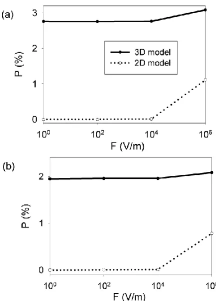
When an external electric field F is applied along the system z-direction, the 2D model (3) of the Rashba spin-orbit interaction can generate some changes in the g-factor components and can stimulate very modest anisotropy in the magnetic response of the system. In Fig. 3 we show that for the 2D model (3) the g-factor anisotropy can reach measurable values only for relatively large external electric fields both for the small and large dots. At the same time within the full 3D description (2) for the small and large quantum dots the electron g-factor anisotropy is gradually growing with increase of the electric field magnitude.
IV. CONCLUSION
In conclusion, using the effective one electronic band Hamiltonian, two different models for Rashba spin-orbit interaction (full 3D and "adiabatic" 2D), and mapping method we simulated the electron g-factors in small self-assembled semiconductor lens shaped quantum dots. Lattice strain, piezoelectric polarization, and external electric fields were taking into account. In this paper we obtained the g -factor components and the -factor anisotropy ratio for two
InxGa1-xAs/GaAs quantum dots of different sizes. We argued that the commonly used two dimensional 2D approximation cannot explain the build-in 3D anisotropy of the electron g -factor in semiconductor quantum dots without external electric fields. Only the full 3D description for the Rashba spin-orbit interaction can lead to reasonable simulation results. At the same time external electric fields of relatively large magnitudes can stimulate and enhance anisotropy in the electronic magnetic response of the quantum dots.
We should note that, using our full 3D description, we are able to obtain the electron g-factor components and the factor anisotropy ratio in good agreement with the experimental observations.
Our computational approach can be applied for the realistic modeling of selective manipulations of isolated and entangled spins in semiconductor quantum dots. This can be potentially useful for further fabrication of nano-system with principally new magnetic properties.
REFERENCES
[1] Semiconductor nanostructures, Editor D. Bimberg, Springer, Berlin, 2008.
[2] G. Konstantatos and E. H. Sargent, “Nanostructured materials for photon detection,” Nature Nanotechnology, vol. 5, no. 6, pp. 391-400, Jun. 2010.
[3] B.C. Lee, O. Voskoboynikov, C.P. Lee, “III-V Semiconductor nano-rings,” Physica E: Low-dimensional Systems and Nanostructures,
vol. 24, no. 1-2, pp. 87-91, Aug. 2004.
[4] Optics of quantum dots and wires, 1st edition, Editors G. W. Bryant and G. S. Solomon, Artech House, MA, 2005.
[5] T. Ihn, Semiconductor Nanostructures: Quantum states and electronic transport, Oxford University Press, Oxford, 2010. [6] Biomedical Nanostructures, Editors K. Gonsalves, C. Halberstadt, C.
T. Laurencin and L. Nair, John Wiley & Sons, Inc., NJ, 2008. [7] S. M. Reimann and M. Maninen, “Electronic structure of quantum
dots,” Review of Modern Physics, vol. 74, no. 4, pp. 1283-1342, Nov. 2002.
[8] F. Boxberg and J. Tulkki, “Theory of the electronic structure and carrier dynamics of strain-induced (Ga, In)As quantum dots,” Reports on Progress in Physics, vol. 70, no. 8, pp. 1425-1471, Jul. 2007. [9] T. D. Ladd, F. Jelezko, R. Laflamme, Y. Nakamura, C. Monroe, and
J. L. O’Brien, “Quantum computers,” Nature, vol. 464, no. 7265, pp. 45-53, Mar. 2010.
[10] C. E. Pryor and M. E. Flatté, “Landé g factors and orbital momentum quenching in semiconductor quantum dots,” Physical Review Letter, vol. 96, no. 2, pp. 026804-1-4, Jan. 2006.
[11] J. Pingenot, C. E. Pryor, and M. E. Flatté, “Electric-field manipulation of the Landé g tensor of a hole in an In0.5Ga0.5As/GaAs
self-assembled quantum dot,” Physical Review B, vol. 84, no. 19, pp. 195403-1-5, Nov. 2011.
[12] Yu. L. Bychkov and E. I. Rashba “Oscillatory effects and the magnetic susceptibility of carriers in inversion layers,” Journal of Physics C: Solid State Physics, vol. 17, no. 33, pp. 6039-6045, Nov. 1984.
[13] E. A. de Andrada e Silva, G. C. La Rocca, and F. Bassani, “Spin-split subbands and magneto-oscillations in III-V asymmetric heterostructures,” Physical Review B, vol. 50, no. 12, pp. 8523-8533, Sep. 1994.
[14] G. Dresselhaus, “Spin-Orbit Coupling Effects in Zinc Blende Structures,” Physical Review, vol. 100, no. 2, pp. 580-586, Oct. 1955.
[15] F.M. Peeters and V.A. Schweigert, “Two-electron quantum disks,”
Physical Review B, vol. 53, no. 3, pp. 1468–1474, Jan. 1996. [16] C. F. Destefani and S. E. Ulloa, “Anisotropic electron g factor in
quantum dots with spin-orbit interaction,” Physical Review B, vol. 71, no. 16, pp. 161303-1-4, Apr. 2005.
[17] M. P. Nowak and B. Szafran, “Singlet-triplet avoided crossings and effective g factor versus spatial orientation of spin-orbit-coupled quantum dots,” Physical Review B, vol. 83, no. 3, pp. 035315-1-8, Jan. 2011.
[18] Y. Liu, F. Cheng, X. J. Li, F. M. Peeters, and Kai Chang, “Tuning of anisotropy in two-electron quantum dots by spin-orbit interactions,”
Applied Physics Letters, vol. 99, no. 3, pp. 032102-1-3, Jul. 2011. [19] S. Prabhakar, J. E. Raynolds, and R. Melnik, “Manipulation of the
Land´e g factor in InAs quantum dots through the application of anisotropic gate potentials: Exact diagonalization, numerical, and perturbation methods,” Physical Review B, vol. 84, no. 15, pp. 155208-1-8, Oct. 2011.
[20] D. Ribeiro-Santos, Fanyao Qu, P. C. Morais, V. Lopez-Richard, and G. E. Marques, “Gate-controlled electron g-factor in lateral quantum dot molecules,” Journal of Applied Physics, vol. 110, no. 12, pp. 124309-1-6, Dec. 2011.
[21] S. Prabhakar and R. Melnik, “Influence of electromechanical effects and wetting layers on band structures of AlN/GaN quantum dots and spin control,” Journal of Applied Physics, vol. 108, no. 6, pp. 064330-1-7, Sep. 2010.
[22] Yiming Li, Jinn-Liang Liu, O. Voskoboynikov, C.P. Lee, S.M. Sze, “Electron energy level calculations for cylindrical narrow gap semiconductor quantum dot,” Computer Physics Communications, vol. 140, no. 3, pp. 399–404, Nov. 2001.
[23] O. Voskoboynikov, Y. Li, H. M. Lu, C. F. Shih, and C. P. Lee, Phys. “Energy states and magetization in nanoscale quantum rings,”
Physical Review B, vol. 66, no. 15, pp. 155306-1-6, Oct. 2002. [24] J. I. Climente, J. Planelles, and J. L. Movilla, “Magnetization of
nanoscopic quantum rings and dots,” Physical Review B, vol. 70, no. 8, pp. 081301-1-4, Aug. 2004.
[25] H. C. Huang, O. Voskoboynikov, and C. P. Lee, “Spin-orbit interaction and electron elastic scattering from impurities in quantum wells,” Physical Review B, vol. 67, no. 19, pp. 195337-1-8, May 2003.
[26] C. Pryor, “Eight-band calculations of strained InAs/GaAs quantum dots compared with one-, four-, and six-band approximations,”
[27] O. Stier, M. Grudmann, and D. Bimberg, “Electronic and optical properties of strained quantum dots modeled by 8-band kp theory,”
Physical Review B, vol. 59, no. 8, pp. 5688-5701, Feb. 1999. [28] L. C. Lew Yan Voon and M. Willatzen, “Electromehanical
phenomena in semiconductor nanostructures,” Journal of Applied Physics, vol. 109, no. 3, pp. 031101-1-24, Mar. 2011.
[29] L. D. Landau and E. M. Lifshitz, Theory of Elasticity. Vol. 7, 1st edition, Pergamon Press, Oxford, 1959.
[30] L. M. Thu and O. Voskoboynikov, “Unusual diamagnetism in semiconductor nano-objects,” Physics Procedia 3, vol. 3, no. 2, pp. 1133-1137, Jan. 2010.
[31] L. M. Thu and O. Voskoboynikov, “Simulation of an Asymmetrical Nano Ring by Mapping of the Realistic Electronic Confinement Potential,” AIP Conference Proceedings, vol. 1233, pp. 952-957, May 2010.
[32] L. M. Thu, W. T. Chiu, and O. Voskoboynikov, “Effect of size and shape dispersion on the averaged magnetic response of ensembles of semiconductor quantum rings,” Physical Review B, vol. 85, no. 20, pp. 205419-1-9, May 2012.
[33] C. Kammerer, S. Sauvage, G. Fishman, P. Boucaud, G. Patriarche, and A. Lemaître, “Mid-infrared intersublevel absorption of vertically electronically coupled InAs quantum dots,” Applied Physics Letters, vol. 87, no. 17, pp. 173113-1-3, Oct. 2005.
[34] I. Vurgaman, J. R. Meyer, and L. R. Ram-Mohan, “Band parameters for III-V compound semiconductors and their alloys,” Journal of Applied Physics, vol. 89, no. 11, pp. 5815-5875, Feb. 2001.
[35] Y. M. Li, O. Voskoboynikov, C. P. Lee, and S. M. Sze, “Computer simulation of electron energy levels for different shape InAs/GaAs semiconductor quantum dots,” Computer Physics Communications, vol. 141, no. 1, pp. 66-72, Nov. 2001.
[36] See: http://www.comsol.com.