Semiconductor Devices and Electronic World
Renu Kasera and M. Z. Khan
1Research Scholar,
DR.C.V.Raman University Kota, Bilaspur, INDIA.
2Associate Professor,
Department of Physics
DR.C.V.Raman University Kota, Bilaspur, INDIA. Corresponding Author: [email protected]
(Received on: April 22, 2019)
ABSTRACT
In this paper an attempt has been made to describe about semiconductor and electronics world. PN junction, zener diode, LED, transistor, photo diode, tunnel diode etc plays pivotal role in electronic world. It has been found that the junction region has a physical thickness that varies with the applied voltage. It has been also observed that semiconductor devices has important role in digital era in the form of IC.
Keywords: PN junction, transistor, voltage, digital era, ICs’.
1. INTRODUCTION
Electronic science began in 1883, when Edison observed that an electric current would pass between the heated filament and a positive mental plate in the vacuum of one of his lamps semiconductor crystal’s are the central components used to process the electrical signals that arise in communication, computation and control systems. It is the electrical behaviors of these device that provides the controlled sources and controlled switches needed on signal processing circuit certain substances like germanium, silicon, carbon etc. are neither good conductors like copper nor insulators like glass. In other words the resistivity of these materials lies between conductors and insulators. Such substances are classified as semiconductors.
The 1950s was a decade of Transistor. It marked the end of the development of sophisticated vacuum tube system and the beginning of the semiconductor age. The age of semiconductor electronics began with the invention of the transistor in 1948. However this ERA originated in earlier work performed between 1920 and 1945. Semiconductor opened the floodgate to further development in electronics. The first integrated circuit (ICs) appeared in the market during the early sixties. Man desire to conquer space accelerated this growth even further the semiconductor age had truly began. Now during the eighties this tremendous growth rate is not only continuing but is accelerating every year. The use of values nearly became obsolete during the sixties. Due to the rapid developments in integrated circuit technology starting from the small scale integration then medium scale integration large scale integration (VLSI) technique even the use of individual transistor in becoming unnecessary the vast changes that have taken place during the last so years can best be understood by noting the reduction in size and price of modern digital computers.
Semiconductor devices are the central components used to process the electrical signal that arise in communication computation and control system as a p-n junction conducts currents easily when forward biased and practically no current flows when it is biased. The P-N junction is the basic building block an which the operation of all semiconductors devices depends certain substances like germanium, silicon, carbon etc, are neither good conductors like copper nor insulators. Such substances are classified as semiconductors. Semiconductors have some useful properties and are being extensively used in electronic circuits. For instance transistor a semiconductor device in fast replacing bulky vacuum tubes in almost all applications .Transistors are only one of the families of semiconductor devices.
Electronics – to most of us, brings to mind, a variety of things from chips and computers to televisions and transistors. In the strictest sense, electronics is the science and technology of motion of charges in a gas, vacuum or semiconductor. The motion of charges confined to a metal only, is not considered electronics. Early in the twentieth century, the electrical engineering dealt with the devices that depended solely on the motion of electrons in metals such as in motors, generators, light bulbs and wire communication system i.e. telephony and telegraphy. Now with the rapid advancement of technology, the electronics engineering has entered in every sphere of life and a large number of materials are used in electronics engineering to perform the various functions. Some of the various functions which are generally required to be performed by the different materials used in electrical and electronics engineering are listed as below:
1. To carry signal from one place to another.
2. To obstruct the flow of electric signal in a particular direction. 3. To store electrical energy.
4. To transfer electrical energy from one circuit to another. 5. To convert one from of an energy into another form. 6. To process the electrical signal.
1. Transmission lines, cables, flexible wire etc.
2. Insulators for overhead conductors, insulation covering for cables and flexible wire transformer oils etc.
3. Capacitors using air, plastic ceramics etc. as dielectric. 4. Transformers.
5. Different kinds of transducers
6. Semiconductor materials for transistors, diodes etc.
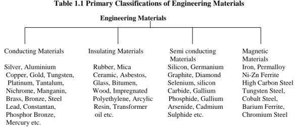
All the primary materials which are commonly used in electrical and electronics engineering can be functionally classified as follows: -
a) Conducting materials b) Insulating materials c) Semi conducting materials d) Magnetic materials
Table 1.1 Primary Classifications of Engineering Materials
More recent advances in the field of electronics include the digital circuits, microprocessor, digital computers, opts electronics, laser technology etc. Today electronics has invaded every walk of life and its application are increasing at a very fast rate. Life today without any electronic gadget will become to drab. However broadly the various applications of electronics may be put into the falling categories –
1. Communication
2. Entertainment electronic 3. Industrial electronic 4. Defense electronic 5. Medical electronic 6. Instrumentation
7. Navigation and Aircraft landing 8. Telemetry
Engineering Materials
Conducting Materials Insulating Materials Semi conducting Magnetic Materials Materials
The P-N junction is of great importance because it is in effect, the control element for semiconductor device. As we know that there are two types of semiconductors, namely; NPN and PNP. Whenever we study in detail then the knowledge of PN junction diode especially electron, hole pair theory , diffusion, forward biasing, reverse biasing, effect of Silicon and Germanium, majority and minority carriers, electrostatic field, depletion region, plugs vital tool. Further it is fully shown different types of characteristics curve of PNP and NPN in common base, common emitter and common collector mode.
2. THEORETICAL CONSIDERATION
The construction of transistor is best understood by two diodes where two diodes are connected back to back. A PNP transistor to two diodes with their cathodes(n-types) connected together to form its base terminal. An NPN transistor is to two diodes with their anodes (p-type) connected together to form its base terminal.
Clearly semiconductor and transistor are widely in study but our main focus is to analyze and emphasize about P-N junction diode which plays key part in PNP-NPN transistor. The diode history is divided into two major periods of time, referred to as the vacuum tubes era and the transistor era. Our main objective is to understand the transistor action, working of partition, characteristics curves in different mode, importance of transistor action, analyses of input/output performance, numbering system, power rating of transistor, lead identification to reach common man in the large interest of society as well as human beings, faithful biasing, inherent variation of transistor parameters, stabilization, stability factor, design of transistor, operating point, med point biasing etc.
In the strictest sense Electronics, is the science and technology of the motion of charges in a gas, vacuum, or semiconductor we view the nature of the discipline of electronics comprise the four C’s-
Communication Computation Control and Components.
The electronic history is divided into two main parts. One is vacuum tube era and another is transistor era. The vacuum tube era spans the first half of the twentieth century.
Electrical and electronics system basically involve charge carriers or electricity. Thousands of years ago when Greeks discovered artificially produced electricity by rubbing some materials, that was the birth of electrical or electronic science. The vacuum tube era spans the first half of the twentieth century, modern electronics took shops technology in this period. In 1904 Fleming invented a two device, the diode, which he called the valve.
this era originated in earlier work performed between 1920 and 1945. When a p-type semiconductor is suitably joined to n-type semiconductor, the contact surface is called P-N junction. Most semiconductor devices contain one or more P-N junctions. When a third doped element is added to crystal diode in such a way that two P-N junctions are formed, the resulting device is known as a transistor. The transistor in entirely new type of electronic device is capable of achieving amplification of weak signals in a fashion comparable and often superior to that realized by vacuum tubes. In another word we can say that a transistor consists of two P-N junctions formed by sand witching either p-type or n-type semiconductor between a pair of opposite types. Thus P-N junction diode really plays key role in transistor era.
3. RESULT AND DISCUSSION
One of the noteworthy things about this field, as in many other areas of technology, is how little the fundamental principles changes over time. Systems are incredibly smaller, current speeds of operation are truly remarkable, and new gadgets surface every day, leaving us to wonder where technology is taking us. However, if we take a moment to consider that the majority of all the devices in use were invented decades ago and that design techniques appearing in texts as far back as the 1930s are still in use, we realize that most of what we see is primarily a steady improvement in constructions techniques, general characteristics, and application techniques rather than the development of new elements and fundamentally new designs. The result is that most of the devices discussed in this text have been around for some time, and that tests on the subject written a decade ago are still good references with content that has not changed very much. The major changes have been in the understanding of how these devices work and their full range of capabilities, and in improved methods of teaching the fundamentals associated with them. The benefit of all this to the new student of the subject is that the material in this text will, we hope, have reached a level where it is relatively easy to grasp and the information will have application for years to come.
is a material that has a conductivity level somewhere between that of a good conductor and that of an insulator. A bonding of atoms, strengthened by the sharing of electrons between neighboring atoms, is called covalent bonding. Increasing temperatures can cause a significant increase in the number of free electrons in a semiconductor material. Most semiconductor materials used in the electronics industry have negative temperature coefficient; that is, the resistance drops with an increase in temperature.
Intrinsic materials are those semiconductors that have very low level of impurities, whereas extrinsic materials are semiconductors that have been exposed to a doping process. An n-type material is formed by adding donor atoms that have five valence electrons to establish a high level of relatively free electrons. In an n-type material, the electron is the majority carrier and the hole is the minority carrier.
A n-type material is formed by adding acceptor atoms with three valence electrons to establish a high level of holes in the material. In a p-type material, the hole is the majority carrier and the electron is the minority carrier. The region near the junction of a diode that has very few carriers is called the depletion region. In the absence of any externally applied bias, the diode current is zero. In the forward-bias region the diode current increases exponentially with increase in voltage across the diode. In the forward-bias region the diode current increases exponentially with increase in voltage across the diode. In the reverse-bias region the diode current is the very small reverse saturation current until Zener breakdown is reached and current will flow in the opposite direction through the diode.
The reverse saturation current ISwill just about double in magnitude for every 10-fold
increase in temperature. The dc resistance of a diode is determined by the ratio of the diode voltage and current at the point of interest and is not sensitive to the shape of the curve. The dc resistance decreases with increase in diode current or voltage.
The maximum power dissipation level of a diode is equal to the product of the diode voltage and current. The capacitance of a diode increases exponentially with increase in the forward-bias voltage. Its lowest levels are in the reverse-bias region. The direction of conduction for a Zener diode is opposite to that of the forward-bias voltage. Its lowest levels are in the reverse-bias region. Light-emitting diodes (LEDs) emit light under forward-bias conditions but require 2V to 4V for good emission.
Semiconductor devices have the following advantages over vacuum tubes: They are a. smaller size
b. more lightweight c. more rugged, and d. more efficient. In addition, they have 1. no warm-up period 2. no heater requirement, and 3. lower operating voltages.
One p-n junction of transistor is forward-biased, whereas the other is reverse biased. The dc emitter current is always the largest current of transistor, whereas the base current is always the a smallest. The emitter current is always the sum of the other two. The collector current is made up of tow components: the majority component and the minority current (also called the leakage current). The arrow in the transistor symbol defines the direction of conventional current flow for the emitter current and thereby defines the direction for the other currents of the device.
A three- terminal device needs two sets of characteristics to completely define its characteristics. In the active region of a transistor, the base-emitter junction is forward-biased, whereas the collector- base junction is reverse-biased. In the cutoff region the base-emitter and collector-base junctions of a transistor are both reverse-biased. In the saturation region the base-emitter and collector-base junctions are forward-biased.
On an average basis, as a first approximation, the base-to-emitter voltage of a operating transistor can be assumed to be 0.7V. The quantity alpha (α) relates the collector and emitter currents and is always close to one. The impedance between terminals of a forward-biased junction is always relatively small, whereas the impedance between terminals of a reverse-biased junction is usually quite large. The arrow in the symbol of an npn transistor points out of the device (not pointing), whereas the arrow points in to the center of the symbol for a pnp transistor (pointing in). For linear amplification purposes, cutoff for the common-emitter configuration will be defined by IC=ICEO.
The quantity beta(β) provides an important relationship between the base and collector currents, and is usually between 50 and 400. The dc beta is defined by a simple ratio of dc currents at an operating point, whereas the ac beta is sensitive to the characteristics in the region of interest. For most applications, however, the two are considered equivalent as a first approximation.
To ensure that a transistor is operating within its maximum power level rating, simply find the product of the collector-to-emitter voltage and the collector current, and compare it to the rated value.
PNPN DEVICES
1.Silicon controlled Rectifier
Within the family of pnpn devices, the silicon –controlled rectifier is of greatest interest. It was first introduced in 1956 by Bell Laboratories. Some of the more common areas of application for SCRs include relay controls, time-delay circuits, regulated power suppliers, static switches, motor controls, choppers, invertors, cycloconverters, battery chargers, protective circuits, heater controls, and phase controls.
2. Basic silicon-Controlled Rectifier Operation
been extended to about 50 kHz, permitting some high-frequency application such as induction heating and ultrasonic clearing.
The phototransistor is a three-terminal device having characteristic very similar to those of a BJT with a base and collector current sensitive to the incident light intensity. The base current that results is essentially linearly related to the applied light with a level almost independent of the voltage across the device until breakdown results.
Opto-isolators contain an infrared LED and a photo detector to provide a linkage between system that does not require a direct connection. The output detector current is less than but linearly related to the applied input LED current. Furthermore, the collector current is essentially independent of the collector-to-emitter voltage.
The PUT (programmable unijunction transistor) is , as the name implies, a device with the characteristics of a UJT but with the added capability of being able to control the firing potential. In general , the peak, valley, and minimum operating voltages of PUTs are less than those of UJTs.
4. CONCLUSION
Semiconductor devices are the central components used to process the electrical signal that arise in communication computation and control system as a p-n junction conducts currents easily when forward biased and practically no current flows when it is biased.
Whit the progress of IC component densities on the silicon chip increased so rapidly that large circuit could be put on a single small silicon chip so the costs and sizes decreased tremendously that led to very fast spread of electronics especially digital electronics components and then the software technology and spurt of communication technologies. So we today find electronics and electronics all around us information technology pace. 1948. is the historical year in the growth of electronics because the superconductor transistor amplifier took birth in this year which heralded the start of the solid stat electronics. So fast mostly all vacuum tube electronics. In 1950s and 1960s more and more semiconductor discrete components and ICs were predicted. At first the circuits were being designed assemble using discrete solid state components than mixed with ICs.
The diode is one of the many component used in electronics circuits another important components is the transistor. It is used for amplifying weak electrical signals . Relatively newer devices like junction filed effect transistor metal oxide semiconductor field effect transistor, silicon controlled rectifier, Unijunction transistor etc. are finding wide application in electronics. All these devises are made of semiconductor materials. So we study tray vacuum tube era to transistors era.
5. REFERENCES
1. D. C. Kulshreshtha Electronic Devices & Circuits D. C. Kulshreshtha, Ravised 2nd Edition,
New age International (P) Ltd. Publishers .
2. G. K. Mithal Khanna Electronic Devices & Circuits- Publishers New Delhi.
3. P. K. Sen Electronic Device, Eastern Economy Edition,Prentice – Hall of India Private Limited (2006).
4. Jacob Millman Integrated Electronics - Christors Helkiyars, Chetan D. Parikh Tata McGraw Hill Publishing Company Ltd. New Delhi.
5. R.S. Anand et al., “A Study into the Applicability of PN Junction to Power Simiconductor
Diode for Faster Reverse Recovery” IEEE, Trans. Electron Devices.
6. B. Ghosh, “ Fundamental Principles of Electronics”, Books and Allied(P), Ltd., Kolkatta, (2016).
7. Boylestad R.L. et al., “ Electronics Devices and Circuit Theory, Pearson”, (2009).
8. D. Chattopadhay et al., “Electronics Fundamentals and Applications”, New Age