1. General
description
The PCF8523 is a CMOS1 Real-Time Clock (RTC) and calendar optimized for low power
consumption. Data is transferred serially via the I2C-bus with a maximum data rate of
1000 kbit/s. Alarm and timer functions are available with the possibility to generate a wake-up signal on an interrupt pin. An offset register allows fine-tuning of the clock. The PCF8523 has a backup battery switch-over circuit, which detects power failures and automatically switches to the battery supply when a power failure occurs.
For a selection of NXP Real-Time Clocks, see Table 56 on page 68
2. Features and benefits
Provides year, month, day, weekday, hours, minutes, and seconds based on a
32.768 kHz quartz crystal
Resolution: seconds to years
Clock operating voltage: 1.0 V to 5.5 V
Low backup current: typical 150 nA at VDD= 3.0 V and Tamb= 25C
2 line bidirectional 1 MHz Fast-mode Plus (Fm+) I2C interface, read D1h, write D0h2
Battery backup input pin and switch-over circuit
Freely programmable timer and alarm with interrupt capability
Selectable integrated oscillator load capacitors for CL= 7 pF or CL= 12.5 pF
Oscillator stop detection function
Internal Power-On Reset (POR)
Open-drain interrupt or clock output pins
Programmable offset register for frequency adjustment
3. Applications
Time keeping application
Battery powered devices
Metering
Rev. 7 — 28 April 2015
Product data sheet
1. The definition of the abbreviations and acronyms used in this data sheet can be found in Section 22. 2. Devices with other I2C-bus slave addresses can be produced on request.
4. Ordering
information
4.1 Ordering options
[1] Bump hardness see Table 53.
5. Marking
Table 1. Ordering information
Type number Package
Name Description Version
PCF8523T SO8 plastic small outline package; 8 leads; body width 3.9 mm
SOT96-1 PCF8523TK HVSON8 plastic thermal enhanced very thin small outline
package; no leads; 8 terminals; body 4 4 0.85 mm
SOT909-1
PCF8523TS TSSOP14 plastic thin shrink small outline package; 14 leads; body width 4.4 mm
SOT402-1
PCF8523U bare die 12 bumps (6-6) PCF8523U
Table 2. Ordering options
Product type number
Sales item (12NC) Orderable part number
IC revision
Delivery form
PCF8523T/1 935293581118 PCF8523T/1,118 1 tape and reel, 13 inch
PCF8523TK/1 935293573118 PCF8523TK/1,118 1 tape and reel, 13 inch
PCF8523TS/1 935291196112 PCF8523TS/1,112 1 tube
935291196118 PCF8523TS/1,118 1 tape and reel, 13 inch
PCF8523U/12AA/1 935293887005 PCF8523U/12AA/1,00 1 chips with bumps[1], sawn wafer on Film
Frame Carrier (FFC)
Table 3. PCF8523U wafer information
Type number Wafer thickness Wafer diameter FFC for wafer size Marking of bad die
PCF8523U/12AA/1 200 m 6 inch 8 inch wafer mapping
Table 4. Marking codes
Type number Marking code
PCF8523T/1 8523T
PCF8523TK/1 8523
PCF8523TS/1 8523TS
6. Block
diagram
Fig 1. Block diagram of PCF8523
DDD
3&) 26&,//$725
N+] ',9,'(5 &/2&.287
,17(55837
,17 32:(521
5(6(7
,&%86 ,17(5)$&( 26&,
6&/ 6'$ 26&2
9%$7
9''
966
&26&,
&26&2
%$77(5< %$&.83 6:,7&+29(5 &,5&875<
&/2&. &$/,%5$7,21 2))6(7
6<67(0 &21752/
5($/7,0( &/2&.
$/$50
7,0(5
,17&/.287 &/.287
7. Pinning
information
7.1 Pinning
Top view. For mechanical details, see Figure 39 on page 56.
Fig 2. Pin configuration for SO8 (PCF8523T)
For mechanical details, see Figure 40 on page 57.
Fig 3. Pin configuration for HVSON8 (PCF8523TK)
Top view. For mechanical details, see Figure 41 on page 58.
Fig 4. Pin configuration for TSSOP14 (PCF8523TS)
3&)7
26&, 9''
26&2 ,17&/.287
9%$7 6&/
966 6'$
DDD DDD 6'$ 966 6&/ 9%$7 ,17&/.287 26&2 9'' 26&, 7UDQVSDUHQWWRSYLHZ WHUPLQDO LQGH[DUHD 3&)7. 3&)76
26&, 9''
26&2 ,17&/.287
QF QF
9%$7 6&/
966 6'$
QF QF ,17 &/.287 DDD
7.2 Pin description
[1] Wire length between quartz and package should be minimized. [2] For manufacturing tests only; do not connect it and do not use it.
[3] The die paddle (exposed pad) is connected to VSS and should be electrically isolated.
[4] The substrate (rear side of the die) is connected to VSS and should be electrically isolated.
[5] The PCF8523 can either drive the CLKOUT or the INT1.
Viewed from active side. For mechanical details, see Figure 42 on page 59.
Fig 5. Pin configuration for PCF8523U
DDD
3&)8
9''
26&,
26&2
9%$7
966
,17 QF
&/.287 6'$ 6&/ QF
,17&/.287
Table 5. Pin description
Input or input/output pins must always be at a defined level (VSS or VDD) unless otherwise specified.
Symbol Pin Type Description SO8
(PCF8523T)
HVSON8 (PCF8523TK)
TSSOP14 (PCF8523TS)
PCF8523U
OSCI 1 1 1 2 input oscillator input;
high-impedance node[1]
OSCO 2 2 2 3 output oscillator output; high-impedance
node[1]
n.c. - - 3, 6, 9, 12[2] 6 and 11[2] - not connected; do not connect
and do not use it as feed through
VBAT 3 3 4 4 supply battery supply voltage
VSS 4 4[3] 5 5[4] supply ground supply voltage
INT2 - - 7 7 output interrupt 2 (open-drain, active
LOW)
CLKOUT[5] - - 8 8 output clock output (open-drain)
SDA 5 5 10 9 input/output serial data input/output
SCL 6 6 11 10 input serial clock input
INT1/CLKOUT[5] 7 7 13 12 output interrupt 1/clock output
(open-drain)
8. Functional
description
The PCF8523 contains:
•
20 8-bit registers with an auto-incrementing address register•
An on-chip 32.768 kHz oscillator with two integrated load capacitors•
A frequency divider, which provides the source clock for the Real-Time Clock (RTC)•
A programmable clock output•
A 1 Mbit/s I2C-bus interface•
An offset register, which allows fine-tuning of the clockAll 20 registers are designed as addressable 8-bit registers although not all bits are implemented.
•
The first three registers (memory address 00h, 01h, and 02h) are used as control andstatus registers
•
The addresses 03h through 09h are used as counters for the clock function (secondsup to years)
•
Addresses 0Ah through 0Dh define the alarm condition•
Address 0Eh defines the offset calibration•
Address 0Fh defines the clock-out mode and the addresses 10h and 12h the timermode
•
Addresses 11h and 13h are used for the timersThe registers Seconds, Minutes, Hours, Days, Weekdays, Months, and Years are all coded in Binary Coded Decimal (BCD) format. Other registers are either bit-wise or standard binary. When one of the RTC registers is read, the contents of all counters are frozen. Therefore, faulty reading of the clock and calendar during a carry condition is prevented.
The PCF8523 has a battery backup input pin and battery switch-over circuit. The battery switch-over circuit monitors the main power supply and switches automatically to the backup battery when a power failure condition is detected. Accurate timekeeping is maintained even when the main power supply is interrupted.
A battery low detection circuit monitors the status of the battery. When the battery voltage goes below a certain threshold value, a flag is set to indicate that the battery must be replaced soon. This ensures the integrity of the data during periods of battery backup.
8.1 Registers overview
The 20 registers of the PCF8523 are auto-incrementing after each read or write data byte up to register 13h. After register 13h, the auto-incrementing will wrap around to address
00h (see Figure 6).
Fig 6. Auto-incrementing of the registers
DDD DGGUHVVUHJLVWHU
K
DXWRLQFUHPHQW
ZUDSDURXQG K
K K K K K
Table 6. Registers overview
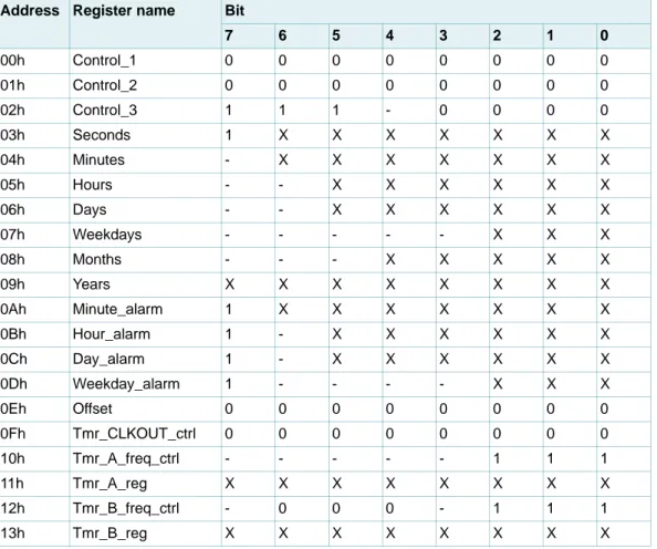
Bit positions labeled as - are not implemented and will return a 0 when read. Bit T must always be written with logic 0.
Address Register name Bit
7 6 5 4 3 2 1 0
Control registers
00h Control_1 CAP_SEL T STOP SR 12_24 SIE AIE CIE
01h Control_2 WTAF CTAF CTBF SF AF WTAIE CTAIE CTBIE
02h Control_3 PM[2:0] - BSF BLF BSIE BLIE
Time and date registers
03h Seconds OS SECONDS (0 to 59)
04h Minutes - MINUTES (0 to 59)
05h Hours - - AMPM HOURS (1 to 12 in 12 hour mode)
HOURS (0 to 23 in 24 hour mode)
06h Days - - DAYS (1 to 31)
07h Weekdays - - - WEEKDAYS (0 to 6)
08h Months - - - MONTHS (1 to 12)
09h Years YEARS (0 to 99)
Alarm registers
0Ah Minute_alarm AEN_M MINUTE_ALARM (0 to 59)
0Bh Hour_alarm AEN_H - AMPM HOUR_ALARM (1 to 12 in 12 hour mode)
- HOUR_ALARM (0 to 23 in 24 hour mode)
0Ch Day_alarm AEN_D - DAY_ALARM (1 to 31)
0Dh Weekday_alarm AEN_W - - - - WEEKDAY_ALARM (0 to 6)
Offset register
CLOCKOUT and timer registers
0Fh Tmr_CLKOUT_ctrl TAM TBM COF[2:0] TAC[1:0] TBC
10h Tmr_A_freq_ctrl - - - TAQ[2:0]
11h Tmr_A_reg T_A[7:0]
12h Tmr_B_freq_ctrl - TBW[2:0] - TBQ[2:0]
13h Tmr_B_reg T_B[7:0]
Table 6. Registers overview …continued
Bit positions labeled as - are not implemented and will return a 0 when read. Bit T must always be written with logic 0.
Address Register name Bit
8.2 Control and status registers
8.2.1 Register Control_1
[1] Default value.
[2] Must always be written with logic 0.
[3] For a software reset, 01011000 (58h) must be sent to register Control_1 (see Section 8.3). Bit SR always returns 0 when read.
Table 7. Control_1 - control and status register 1 (address 00h) bit description
Bit Symbol Value Description
7 CAP_SEL internal oscillator capacitor selection for quartz crystals with a corresponding load capacitance
0[1] 7 pF
1 12.5 pF
6 T 0[1][2] unused
5 STOP 0[1] RTC time circuits running
1 RTC time circuits frozen;
RTC divider chain flip-flops are asynchronously set logic 0;
CLKOUT at 32.768 kHz, 16.384 kHz, or 8.192 kHz is still available
4 SR 0[1][3] no software reset
1 initiate software reset
3 12_24 0[1] 24 hour mode is selected
1 12 hour mode is selected
2 SIE 0[1] second interrupt disabled
1 second interrupt enabled
1 AIE 0[1] alarm interrupt disabled
1 alarm interrupt enabled
0 CIE 0[1] no correction interrupt generated
1 interrupt pulses are generated at every correction cycle (see Section 8.8)
8.2.2 Register Control_2
[1] Default value.
Table 8. Control_2 - control and status register 2 (address 01h) bit description
Bit Symbol Value Description
7 WTAF 0[1] no watchdog timer A interrupt generated
1 flag set when watchdog timer A interrupt generated; flag is read-only and cleared by reading register Control_2
6 CTAF 0[1] no countdown timer A interrupt generated
1 flag set when countdown timer A interrupt generated; flag must be cleared to clear interrupt
5 CTBF 0[1] no countdown timer B interrupt generated
1 flag set when countdown timer B interrupt generated; flag must be cleared to clear interrupt
4 SF 0[1] no second interrupt generated
1 flag set when second interrupt generated; flag must be cleared to clear interrupt
3 AF 0[1] no alarm interrupt generated
1 flag set when alarm triggered; flag must be cleared to clear interrupt
2 WTAIE 0[1] watchdog timer A interrupt is disabled
1 watchdog timer A interrupt is enabled
1 CTAIE 0[1] countdown timer A interrupt is disabled
1 countdown timer A interrupt is enabled
0 CTBIE 0[1] countdown timer B interrupt is disabled
8.2.3 Register Control_3
[1] Default value is 111. [2] Default value.
Table 9. Control_3 - control and status register 3 (address 02h) bit description
Bit Symbol Value Description
7 to 5 PM[2:0] see Table 11[1] battery switch-over and battery low detection
control
4 - - unused
3 BSF 0[2] no battery switch-over interrupt generated
1 flag set when battery switch-over occurs; flag must be cleared to clear interrupt
2 BLF 0[2] battery status ok
1 battery status low; flag is read-only
1 BSIE 0[2] no interrupt generated from battery switch-over
flag, BSF
1 interrupt generated when BSF is set
0 BLIE 0[2] no interrupt generated from battery low
flag, BLF
8.3 Reset
A reset is automatically generated at power-on. A reset can also be initiated with the software reset command. Software reset command means setting bits 6, 4, and 3 in register Control_1 (00h) logic 1 and all other bits logic 0 by sending the bit sequence
01011000 (58h), see Figure 7.
Fig 7. Software reset command
V $ $ $ 36
6'$
6&/
LQWHUQDO UHVHWVLJQDO
VODYHDGGUHVVE\WH 5: DGGUHVVK VRIWZDUHUHVHWK
DDD
Table 10. Register reset values
Bits labeled X are undefined at power-on and unchanged by subsequent resets. Bits labeled - are not implemented.
Address Register name Bit
7 6 5 4 3 2 1 0
00h Control_1 0 0 0 0 0 0 0 0
01h Control_2 0 0 0 0 0 0 0 0
02h Control_3 1 1 1 - 0 0 0 0
03h Seconds 1 X X X X X X X
04h Minutes - X X X X X X X
05h Hours - - X X X X X X
06h Days - - X X X X X X
07h Weekdays - - - X X X
08h Months - - - X X X X X
09h Years X X X X X X X X
0Ah Minute_alarm 1 X X X X X X X
0Bh Hour_alarm 1 - X X X X X X
0Ch Day_alarm 1 - X X X X X X
0Dh Weekday_alarm 1 - - - - X X X
0Eh Offset 0 0 0 0 0 0 0 0
0Fh Tmr_CLKOUT_ctrl 0 0 0 0 0 0 0 0
10h Tmr_A_freq_ctrl - - - 1 1 1
11h Tmr_A_reg X X X X X X X X
12h Tmr_B_freq_ctrl - 0 0 0 - 1 1 1
After reset, the following mode is entered:
•
32.768 kHz CLKOUT active•
24 hour mode is selected•
Register Offset is set logic 0•
No alarms set•
Timers disabled•
No interrupts enabled•
Battery switch-over is disabled•
Battery low detection is disabled•
7 pF of internal oscillator capacitor selected8.4 Interrupt function
Active low interrupt signals are available at pin INT1/CLKOUT and INT2. Pin
INT1/CLKOUT has both functions of INT1 and CLKOUT combined, that is that either the CLKOUT or the INT1 can be used. Therefore the usage of INT1 requires that CLKOUT is disabled.
INT1 Interrupt output may be sourced from different places:
•
Second timer•
Timer A•
Timer B•
Alarm•
Battery switch-over•
Battery low detection•
Clock offset correction pulseINT2 interrupt output is sourced only from timer B:
The control bit TAM (register Tmr_CLKOUT_ctrl) is used to configure whether the interrupts generated from the second interrupt timer and timer A are pulsed signals or a permanently active signal. The control bit TBM (register Tmr_CLKOUT_ctrl) is used to configure whether the interrupt generated from timer B is a pulsed signal or a permanently active signal. All the other interrupt sources generate a permanently active interrupt signal, which follows the status of the corresponding flags.
•
The flags SF, CTAF, CTBF, AF, and BSF can be cleared by using the interface•
WTAF is read only. Reading of the register Control_2 (01h) automatically resetsWTAF (WTAF = 0) and clears the interrupt
•
The flag BLF is read only. It is cleared automatically from the battery low detectionWhen SIE, CTAIE, WTAIE, CTBIE, AIE, CIE, BSIE, BLIE, and clock-out are disabled, then INT1 remains high-impedance. When CTBIE is disabled, then INT2 remains high-impedance.
Fig 8. Interrupt block diagram
%/)%$77(5< /2:)/$* 6(7 VHWEDWWHU\ ORZIODJ%/) WRLQWHUIDFH UHDG%/) %/,( DDD IURPEDWWHU\ ORZGHWHFWLRQ FLUFXLWFOHDU%/) &/($5 %6)%$77(5< )/$* 6(7 VHWEDWWHU\ IODJ%6) WRLQWHUIDFH UHDG%6) %6,( IURPLQWHUIDFH FOHDU%6) &/($5 38/6( *(1(5$725 6(7 RIIVHWFLUFXLW DGGVXEWUDFWSXOVH &,( IURPLQWHUIDFH FOHDU&,( &/($5 $)$/$50 )/$* 6(7 VHWDODUP IODJ$) WRLQWHUIDFH UHDG$) $,( IURPLQWHUIDFH FOHDU$) &/($5 :7$) :$7&+'2* 7,0(5)/$* 6(7 :$7&+'2* &2817(5$ WRLQWHUIDFH UHDG:7$) 0&8ORDGLQJ ZDWFKGRJFRXQWHU RUUHDGLQJ:7$) &/($5 &7$) &2817'2:1 7,0(5$)/$* 6(7 &2817'2:1 &2817(5$ WRLQWHUIDFH UHDG&7$) &7$,( ,17 IURPLQWHUIDFH FOHDU&7$) &/($5 38/6( *(1(5$725 75,**(5 &/($5 6) 6(&21')/$* 6(7 6(&21'6&2817(5 WRLQWHUIDFH
UHDG6) 6,(
IURPLQWHUIDFH FOHDU6) &/($5 6,( 38/6( *(1(5$725
75,**(5 &/($5 7$0
7$0 &/.287 ,17&/.287 (1$%/( 7$& (1$%/( 7$& 38/6( *(1(5$725 75,**(5 &/($5 :7$,( 7$0 &7%) &2817'2:1 7,0(5%)/$* 6(7 &2817'2:1 &2817(5% WRLQWHUIDFH
UHDG&7%) &7%,( IURPLQWHUIDFH FOHDU&7%) &/($5 38/6( *(1(5$725 75,**(5 &/($5 7%0 (1$%/(
8.5 Power management functions
The PCF8523 has two power supply pins:
•
VDD - the main power supply input pin•
VBAT - the battery backup input pinThe PCF8523 has two power management functions implemented:
•
Battery switch-over function•
Battery low detection functionThe power management functions are controlled by the control bits PM[2:0] in register Control_3 (02h):
[1] When the battery switch-over function is disabled, the PCF8523 works only with the power supply VDD.
[2] When the battery switch-over function is disabled, the PCF8523 works only with the power supply VDD and
the battery low detection function is disabled. VBAT must be put to VDD.
[3] Default value.
8.5.1 Standby mode
When the device is first powered up from the battery (VBAT) but without a main supply
(VDD), the PCF8523 automatically enters the standby mode. In standby mode, the
PCF8523 does not draw any power from the backup battery until the device is powered up
from the main power supply VDD. Thereafter, the device switches over to battery backup
mode whenever the main power supply VDD is lost.
It is also possible to enter into standby mode when the chip is already supplied by the
main power supply VDD and a backup battery is connected. To enter the standby mode,
the power management control bits PM[2:0] have to be set logic 111. Then the main
power supply VDD must be removed. As a result of it, the PCF8523 enters the standby
mode and does not draw any current from the backup battery before it is powered up
again from main supply VDD.
Table 11. Power management function control bits
PM[2:0] Function
000 battery switch-over function is enabled in standard mode; battery low detection function is enabled
001 battery switch-over function is enabled in direct switching mode; battery low detection function is enabled
010,011[1] battery switch-over function is disabled - only one power supply (V DD);
battery low detection function is enabled
100 battery switch-over function is enabled in standard mode; battery low detection function is disabled
101 battery switch-over function is enabled in direct switching mode; battery low detection function is disabled
110 not allowed
111[2][3] battery switch-over function is disabled - only one power supply (V DD);
8.5.2 Battery switch-over function
The PCF8523 has a backup battery switch-over circuit. It monitors the main power supply
VDD and switches automatically to the backup battery when a power failure condition is
detected.
One of two operation modes can be selected:
•
Standard mode: the power failure condition happens when: VDD < VBAT AND VDD< Vth(sw)bat•
Direct switching mode: the power failure condition happens when VDD < VBAT.Direct switching from VDD to VBAT without requiring VDD to drop below Vth(sw)bat
Vth(sw)bat is the battery switch threshold voltage. Typical value is 2.5 V.
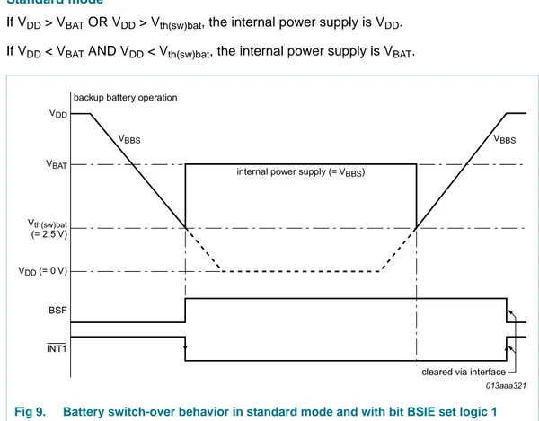
Generation of interrupts from the battery switch-over is controlled via the BSIE bit (see register Control_2). If BSIE is enabled, the INT1 follows the status of bit BLF (register Control_3). Clearing BLF immediately clears INT1.
When a power failure condition occurs and the power supply switches to the battery, the following sequence occurs:
1. The battery switch flag BSF (register Control_3) is set logic 1
2. An interrupt is generated if the control bit BSIE (register Control_3) is enabled The battery switch flag BSF can be cleared by using the interface after the power supply
has switched to VDD. It must be cleared to clear the interrupt.
The interface is disabled in battery backup operation:
•
Interface inputs are not recognized, preventing extraneous data being written to thedevice
8.5.2.1 Standard mode
If VDD > VBAT OR VDD> Vth(sw)bat, the internal power supply is VDD.
If VDD < VBAT AND VDD< Vth(sw)bat, the internal power supply is VBAT.
Fig 9. Battery switch-over behavior in standard mode and with bit BSIE set logic 1 (enabled)
DDD LQWHUQDOSRZHUVXSSO\ 9%%6
FOHDUHGYLDLQWHUIDFH EDFNXSEDWWHU\RSHUDWLRQ
%6) 9WKVZEDW
9
9'' 9 9%$7 9''
9%%6 9%%6
8.5.2.2 Direct switching mode
If VDD > VBAT the internal power supply is VDD.
If VDD < VBAT the internal power supply is VBAT.
The direct switching mode is useful in systems where VDD is higher than VBAT at all times
(for example, VDD = 5 V, VBAT = 3.5 V). If the VDD and VBAT values are similar (for
example, VDD = 3.3 V, VBAT3.0 V), the direct switching mode is not recommended. In
direct switching mode, the power consumption is reduced compared to the standard mode
because the monitoring of VDD and Vth(sw)bat is not performed.
8.5.2.3 Battery switch-over disabled, only one power supply (VDD)
When the battery switch-over function is disabled:
•
The power supply is applied on the VDD pin•
The VBAT pin must be connected to VDD•
The battery flag (BSF) is always logic 08.5.3 Battery low detection function
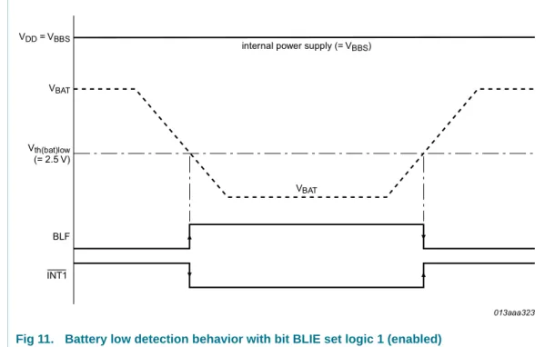
The PCF8523 has a battery low detection circuit, which monitors the status of the battery VBAT.
Generation of interrupts from the battery low detection is controlled via bit BLIE (register Control_3). If BLIE is enabled, the INT1 follows the status of bit BLF (register Control_3).
When VBAT drops below the threshold value Vth(bat)low (typically 2.5 V), the BLF flag
(register Control_3) is set to indicate that the battery is low and that it must be replaced. Monitoring of the battery voltage also occurs during battery operation.
Fig 10. Battery switch-over behavior in direct switching mode and with bit BSIE set logic 1 (enabled)
DDD LQWHUQDOSRZHUVXSSO\ 9%%6
FOHDUHGYLDLQWHUIDFH EDFNXSEDWWHU\RSHUDWLRQ
%6) 9WKVZEDW
9
9'' 9 9%$7 9''
9%%6 9%%6
An unreliable battery does not ensure data integrity during periods of backup battery operation.
When VBAT drops below the threshold value Vth(bat)low, the following sequence occurs (see
Figure 11):
1. The battery low flag BLF is set logic 1
2. An interrupt is generated if the control bit BLIE (register Control_3) is enabled. The interrupt remains active until the battery is replaced (BLF set logic 0) or when bit BLIE is disabled (BLIE set logic 0)
3. The flag BLF (register Control_3) remains logic 1 until the battery is replaced. BLF cannot be cleared using the interface. It is cleared automatically by the battery low detection circuit when the battery is replaced
8.6 Time and date registers
Most of these registers are coded in the Binary Coded Decimal (BCD) format. BCD is used to simplify application use. An example is shown for the array SECONDS in
Table 13.
Fig 11. Battery low detection behavior with bit BLIE set logic 1 (enabled)
DDD LQWHUQDOSRZHUVXSSO\ 9%%6
9%$7
%/) 9WKEDWORZ
9 9%$7 9'' 9%%6
8.6.1 Register Seconds
[1] Start-up value.
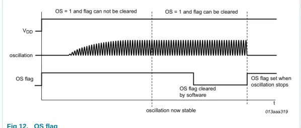
8.6.1.1 Oscillator STOP flag
The OS flag is set whenever the oscillator is stopped (see Figure 12). The flag remains
set until cleared by using the interface. When the oscillator is not running, then the OS flag cannot be cleared. This method can be used to monitor the oscillator.
The oscillator may be stopped, for example, by grounding one of the oscillator pins, OSCI or OSCO. The oscillator is also considered to be stopped during the time between power-on and stable crystal resonance. This time may be in a range of 200 ms to 2 s, depending on crystal type, temperature, and supply voltage. At power-on, the OS flag is always set.
Table 12. Seconds - seconds and clock integrity status register (address 03h) bit description
Bit Symbol Value Place value Description
7 OS 0 - clock integrity is guaranteed
1[1] - clock integrity is not guaranteed;
oscillator has stopped or been interrupted
6 to 4 SECONDS 0 to 5 ten’s place actual seconds coded in BCD format
3 to 0 0 to 9 unit place
Table 13. SECONDS coded in BCD format
Seconds value in decimal
Upper-digit (ten’s place) Digit (unit place)
Bit Bit
6 5 4 3 2 1 0
00 0 0 0 0 0 0 0
01 0 0 0 0 0 0 1
02 0 0 0 0 0 1 0
: : : : : : : :
09 0 0 0 1 0 0 1
10 0 0 1 0 0 0 0
: : : : : : : :
58 1 0 1 1 0 0 0
8.6.2 Register Minutes
8.6.3 Register Hours
[1] Hour mode is set by bit 12_24 in register Control_1 (see Table 7).
8.6.4 Register Days
[1] If the year counter contains a value, which is exactly divisible by 4 (including the year 00), the PCF8523 compensates for leap years by adding a 29th day to February.
Fig 12. OS flag
DDD 26 DQGIODJFDQQRWEHFOHDUHG 26 DQGIODJFDQEHFOHDUHG
W 9''
RVFLOODWLRQ
26IODJ
26IODJFOHDUHG E\VRIWZDUH
26IODJVHWZKHQ RVFLOODWLRQVWRSV
RVFLOODWLRQQRZVWDEOH
Table 14. Minutes - minutes register (address 04h) bit description
Bit Symbol Value Place value Description
7 - - - unused
6 to 4 MINUTES 0 to 5 ten’s place actual minutes coded in BCD format
3 to 0 0 to 9 unit place
Table 15. Hours - hours register (address 05h) bit description
Bit Symbol Value Place value Description
7 to 6 - - - unused
12 hour mode[1]
5 AMPM 0 - indicates AM
1 - indicates PM
4 HOURS 0 to 1 ten’s place actual hours in 12 hour mode
coded in BCD format
3 to 0 0 to 9 unit place
24 hour mode[1]
5 to 4 HOURS 0 to 2 ten’s place actual hours in 24 hour mode coded in BCD format
3 to 0 0 to 9 unit place
Table 16. Days - days register (address 06h) bit description
Bit Symbol Value Place value Description
7 to 6 - - - unused
5 to 4 DAYS[1] 0 to 3 ten’s place actual day coded in BCD format
8.6.5 Register Weekdays
[1] Definition may be reassigned by the user.
8.6.6 Register Months
Table 17. Weekdays - weekdays register (address 07h) bit description
Bit Symbol Value Description
7 to 3 - - unused
2 to 0 WEEKDAYS 0 to 6 actual weekday, values seeTable 18
Table 18. Weekday assignments
Day[1] Bit
2 1 0
Sunday 0 0 0
Monday 0 0 1
Tuesday 0 1 0
Wednesday 0 1 1
Thursday 1 0 0
Friday 1 0 1
Saturday 1 1 0
Table 19. Months - months register (address 08h) bit description
Bit Symbol Value Place value Description
7 to 5 - - - unused
4 MONTHS 0 to 1 ten’s place actual month coded in BCD
format; assignments see Table 20
3 to 0 0 to 9 unit place
Table 20. Month assignments in BCD format
Month Upper-digit (ten’s place)
Digit (unit place) Bit Bit
4 3 2 1 0
January 0 0 0 0 1
February 0 0 0 1 0
March 0 0 0 1 1
April 0 0 1 0 0
May 0 0 1 0 1
June 0 0 1 1 0
July 0 0 1 1 1
August 0 1 0 0 0
September 0 1 0 0 1
October 1 0 0 0 0
November 1 0 0 0 1
8.6.7 Register Years
8.6.8 Data flow of the time function
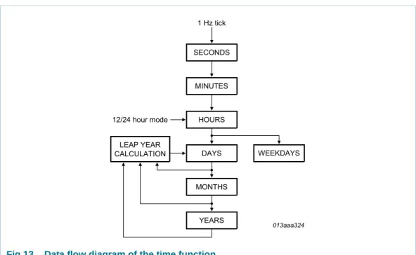
Figure 13 shows the data flow and data dependencies starting from the 1 Hz clock tick.
During read/write operations, the time counting circuits (memory locations 03h through 09h) are blocked.
The blocking prevents:
•
Faulty reading of the clock and calendar during a carry condition•
Incrementing the time registers during the read cycleAfter the read/write-access is completed, the time circuit is released again and any pending request to increment the time counters that occurred during the read/write access is serviced. A maximum of one request can be stored; therefore, all accesses must be
completed within 1 second (see Figure 14).
Table 21. Years - years register (09h) bit description
Bit Symbol Value Place value Description
7 to 4 YEARS 0 to 9 ten’s place actual year coded in BCD format
3 to 0 0 to 9 unit place
Fig 13. Data flow diagram of the time function
Fig 14. Access time for read/write operations
DDD +]WLFN
KRXUPRGH
:((.'$<6 6(&21'6
0,187(6
+2856
'$<6 /($3<($5
&$/&8/$7,21
0217+6
<($56
WV
DDD
6/$9($''5(66 '$7$ '$7$ 6723
Because of this method, it is very important to make a read or write access in one go, that is, setting or reading seconds through to years should be made in one single access. Failing to comply with this method could result in the time becoming corrupted.
As an example, if the time (seconds through to hours) is set in one access and then in a second access the date is set, it is possible that the time will increment between the two accesses. A similar problem exists when reading. A rollover may occur between reads thus giving the minutes from one moment and the hours from the next.
8.7 Alarm registers
The registers at addresses 0Ah through 0Dh contain the alarm information.
8.7.1 Register Minute_alarm
[1] Default value.
8.7.2 Register Hour_alarm
[1] Default value.
[2] Hour mode is set by bit 12_24 in register Control_1 (see Table 7).
Table 22. Minute_alarm - minute alarm register (address 0Ah) bit description
Bit Symbol Value Place value Description
7 AEN_M 0 - minute alarm is enabled
1[1] - minute alarm is disabled
6 to 4 MINUTE_ALARM 0 to 5 ten’s place minute alarm information coded in BCD format
3 to 0 0 to 9 unit place
Table 23. Hour_alarm - hour alarm register (address 0Bh) bit description
Bit Symbol Value Place value Description
7 AEN_H 0 - hour alarm is enabled
1[1] - hour alarm is disabled
6 - - - unused
12 hour mode[2]
5 AMPM 0 - indicates AM
1 - indicates PM
4 HOUR_ALARM 0 to 1 ten’s place hour alarm information in 12 hour mode coded in BCD format
3 to 0 0 to 9 unit place
24 hour mode[2]
5 to 4 HOURS 0 to 2 ten’s place hour alarm information in 24 hour mode coded in BCD format
8.7.3 Register Day_alarm
[1] Default value.
8.7.4 Register Weekday_alarm
[1] Default value.
8.7.5 Alarm flag
Table 24. Day_alarm - day alarm register (address 0Ch) bit description
Bit Symbol Value Place value Description
7 AEN_D 0 - day alarm is enabled
1[1] - day alarm is disabled
6 - - - unused
5 to 4 DAY_ALARM 0 to 3 ten’s place day alarm information coded in BCD format
3 to 0 0 to 9 unit place
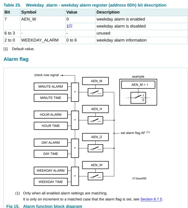
Table 25. Weekday_alarm - weekday alarm register (address 0Dh) bit description
Bit Symbol Value Description
7 AEN_W 0 weekday alarm is enabled
1[1] weekday alarm is disabled
6 to 3 - - unused
2 to 0 WEEKDAY_ALARM 0 to 6 weekday alarm information
(1) Only when all enabled alarm settings are matching.
It is only on increment to a matched case that the alarm flag is set, see Section 8.7.5.
Fig 15. Alarm function block diagram
DDD :((.'$<$/$50
$(1B:
:((.'$<7,0( '$<$/$50
$(1B'
'$<7,0( +285$/$50
$(1B+
+2857,0( 0,187($/$50
$(1B0
0,187(7,0( FKHFNQRZVLJQDO
VHWDODUPIODJ$)
$(1B0 H[DPSOH
When one or several alarm registers are loaded with a valid minute, hour, day, or weekday value and its corresponding alarm enable bit (AEN_x) is logic 0, then that information is compared with the current minute, hour, day, and weekday value. When all enabled comparisons first match, the alarm flag, AF (register Control_2), is set logic 1. The generation of interrupts from the alarm function is controlled via bit AIE (register Control_1). If bit AIE is enabled, then the INT1 pin follows the condition of bit AF. AF remains set until cleared by the interface. Once AF has been cleared, it will only be set again when the time increments to match the alarm condition once more. Alarm registers, which have their AEN_x bit logic 1 are ignored. The generation of interrupts from the
alarm function is described more detailed in Section 8.4.
Table 26 and Table 27 show an example for clearing bit AF. Clearing the flag is made by a write command, therefore bits 2, 1, and 0 must be re-written with their previous values. Repeatedly re-writing these bits has no influence on the functional behavior.
To prevent the timer flags being overwritten while clearing bit AF, logic AND is performed during a write access. A flag is cleared by writing logic 0 while a flag is not cleared by writing logic 1. Writing logic 1 results in the flag value remaining unchanged.
Table 27 shows what instruction must be sent to clear bit AF. In this example, bit CTAF, CTBF, and bit SF are unaffected.
[1] The bits labeled as - have to be rewritten with the previous values.
8.7.6 Alarm interrupts
Generation of interrupts from the alarm function is controlled via the bit AIE (register Control_1). If AIE is enabled, the INT1 follows the status of bit AF (register Control_2). Clearing AF immediately clears INT1. No pulse generation is possible for alarm interrupts.
Example where only the minute alarm is used and no other interrupts are enabled.
Fig 16. Alarm flag timing
Table 26. Flag location in register Control_2
Register Bit
7 6 5 4 3 2 1 0
Control_2 WTAF CTAF CTBF SF AF - -
-Table 27. Example to clear only AF (bit 3)
Register Bit[1]
7 6 5 4 3 2 1 0
Control_2 0 1 1 1 0 - -
-DDI
PLQXWHDODUP PLQXWHVFRXQWHU
$)
,17ZKHQ$,(
Example where only the minute alarm is used and no other interrupts are enabled.
Fig 17. AF timing
DDD
PLQXWHFRXQWHU
PLQXWHDODUP
$)
,17
6&/
LQVWUXFWLRQ
8.8 Register Offset
The PCF8523 incorporates an offset register (address 0Eh), which can be used to implement several functions, like:
•
Aging adjustment•
Temperature compensation•
Accuracy tuning[1] Default value.
For MODE = 0, each LSB introduces an offset of 4.34 ppm. For MODE = 1, each LSB introduces an offset of 4.069 ppm. The values of 4.34 ppm and 4.069 ppm are based on a nominal 32.768 kHz clock. The offset value is coded in two’s complement giving a range
of +63 LSB to64 LSB.
[1] Default mode.
The correction is made by adding or subtracting clock correction pulses, thereby changing the period of a single second.
It is possible to monitor when correction pulses are applied. To enable correction interrupt generation, bit CIE (register Control_1) has to be set logic 1. At every correction cycle a
1⁄
4096s pulse is generated on pin INTx. If multiple correction pulses are applied, a 1⁄4096s
interrupt pulse is generated for each correction pulse applied.
8.8.1 Correction when MODE = 0
The correction is triggered once per two hours and then correction pulses are applied
Table 28. Offset - offset register (address 0Eh) bit description
Bit Symbol Value Description
7 MODE 0[1] offset is made once every two hours
1 offset is made once every minute 6 to 0 OFFSET[6:0] see Table 29 offset value
Table 29. Offset values (in period time, not frequency)
OFFSET[6:0] Offset value in decimal
Offset value in ppm Every two hours (MODE = 0)
Every minute (MODE = 1)
0111111 +63 +273.420 +256.347
0111110 +62 +269.080 +252.278
: : : :
0000010 +2 +8.680 +8.138
0000001 +1 +4.340 +4.069
0000000 0[1] 0[1] 0[1]
1111111 1 4.340 4.069
1111110 2 8.680 8.138
: : : :
1000001 63 273.420 256.347
[1] The correction pulses on pin INT1 are 1⁄ 64s wide.
In MODE = 0, any timer or clock output using a frequency below 64 Hz is affected by the
clock correction (see Table 31).
8.8.2 Correction when MODE = 1
The correction is triggered once per minute and then correction pulses are applied once per second up to a maximum of 60 pulses. When correction values greater than 60 pulses
are used, additional correction pulses are made in the 59th second.
Clock correction is made more frequently in MODE = 1; however, this can result in higher power consumption.
Table 30. Correction pulses for MODE = 0
Correction value Update every nth hour Minute Correction pulses on
INT1 per minute[1]
+1 or 1 2 00 1
+2 or 2 2 00 and 01 1
+3 or 3 2 00, 01, and 02 1
: : : :
+59 or 59 2 00 to 58 1
+60 or 60 2 00 to 59 1
+61 or 61 2 00 to 59 1
2nd and next hour 00 1
+62 or 62 2 00 to 59 1
2nd and next hour 00 and 01 1
+63 or 63 2 00 to 59 1
2nd and next hour 00, 01, and 02 1
64 2 00 to 59 1
2nd and next hour 00, 01, 02, and 03 1
Table 31. Effect of clock correction for MODE = 0
CLKOUT frequency (Hz) Effect of correction Timer source clock frequency (Hz)
Effect of correction
32768 no effect 4096 no effect
16384 no effect 64 no effect
8192 no effect 1 affected
4096 no effect 1⁄
60 affected
1024 no effect 1⁄
3600 affected
32 affected -
-[1] The correction pulses on pin INTx are 1⁄
4096s wide. For multiple pulses, they are repeated at an interval of 1⁄
2048s.
In MODE = 1, clock outputs and timer source clocks affected by the clock correction are
as shownin Table 33.
8.8.3 Offset calibration workflow
The calibration offset has to be calculated based on the time. Figure 18 shows the
workflow how the offset register values can be calculated:
Table 32. Correction pulses for MODE = 1
Correction value Update every nth
minute
Second Correction pulses on INT1 per second[1]
+1 or 1 2 00 1
+2 or 2 2 00 and 01 1
+3 or 3 2 00, 01, and 02 1
: : : :
+59 or 59 2 00 to 58 1
+60 or 60 2 00 to 59 1
+61 or 61 2 00 to 58 1
2 59 2
+62 or 62 2 00 to 58 1
2 59 2
+63 or 63 2 00 to 58 1
2 59 4
64 2 00 to 58 1
2 59 5
Table 33. Effect of clock correction for MODE = 1
CLKOUT frequency (Hz) Effect of correction Timer source clock frequency (Hz)
Effect of correction
32768 no effect 4096 no effect
16384 no effect 64 affected
8192 no effect 1 affected
4096 no effect 1⁄
60 affected
1024 no effect 1⁄
3600 affected
32 affected -
-8.9 Timer function
The PCF8523 has three timers:
•
Timer A can be used as a watchdog timer or a countdown timer (see Section 8.9.2). Itcan be configured by using TAC[1:0] in the Tmr_CLKOUT_ctrl register (0Fh)
•
Timer B can be used as a countdown timer (see Section 8.9.3). It can be configuredby using TBC in the Tmr_CLKOUT_ctrl register (0Fh)
•
Second interrupt timer is used to generate an interrupt once per second (seeSection 8.9.4)
Timer A and timer B both have five selectable source clocks allowing for countdown periods from less than 1 ms to 255 h. To control the timer functions and timer output, the registers 01h, 0Fh, 10h, 11h, 12h, and 13h are used.
Fig 18. Offset calibration calculation workflow
0HDVXUHWKHIUHTXHQF\RQSLQ&/.287 IPHDV
&RQYHUWWRWLPH WPHDV IPHDV
&DOFXODWHWKHGLIIHUHQFHWRWKHLGHDO SHULRGRI 'PHDV WPHDV
&DOFXODWHWKHSSPGHYLDWLRQFRPSDUHG WRWKHPHDVXUHGYDOXH (SSP î'PHDVWPHDV
&DOFXODWHWKHRIIVHWUHJLVWHUYDOXH 0RGH ORZSRZHU 2IIVHWYDOXH (SSP 0RGH IDVWFRUUHFWLRQ 2IIVHWYDOXH (SSP
DDD
([DPSOH +]
V
V
SSP
FRUUHFWLRQSXOVHV
DUHQHHGHG
FRUUHFWLRQSXOVHV
8.9.1 Timer registers
8.9.1.1 Register Tmr_CLKOUT_ctrl and clock output
[1] Default value.
8.9.1.2 CLKOUT frequency selection
Clock output operation is controlled by the COF[2:0] in the Tmr_CLKOUT_ctrl register.
Frequencies of 32.768 kHz (default) down to 1 Hz can be generated (see Table 35) for
use as a system clock, microcontroller clock, input to a charge pump, or for calibration of the oscillator.
A programmable square wave is available at pin INT1/CLKOUT and pin CLKOUT, which are both open-drain outputs. Pin INT1/CLKOUT has both functions of INT1 and CLKOUT combined.
The duty cycle of the selected clock is not controlled but due to the nature of the clock generation, all clock frequencies except 32.768 kHz have a duty cycle of 50 : 50. The STOP bit function can also affect the CLKOUT signal, depending on the selected frequency. When STOP is active, the INT1/CLKOUT and CLKOUT pins are
high-impedance for all frequencies except of 32.768 kHz, 16.384 kHz and 8.192 kHz. For
more details, see Section 8.10.
Table 34. Tmr_CLKOUT_ctrl - timer and CLKOUT control register (address 0Fh) bit description
Bit Symbol Value Description
7 TAM 0[1] permanent active interrupt for timer A and for
the second interrupt timer
1 pulsed interrupt for timer A and the second interrupt timer
6 TBM 0[1] permanent active interrupt for timer B
1 pulsed interrupt for timer B 5 to 3 COF[2:0] see Table 35 CLKOUT frequency selection 2 to 1 TAC[1:0] 00[1] to 11 timer A is disabled
01 timer A is configured as countdown timer if CTAIE (register Control_2) is set logic 1, the interrupt is activated when the countdown timed out
10 timer A is configured as watchdog timer if WTAIE (register Control_2) is set logic 1, the interrupt is activated when timed out
0 TBC 0[1] timer B is disabled
1 timer B is enabled
if CTBIE (register Control_2) is set logic 1, the interrupt is activated when the countdown timed out
[1] Duty cycle definition: % HIGH-level time : % LOW-level time. [2] Default value.
[3] Clock frequencies may be affected by offset correction.
8.9.1.3 Register Tmr_A_freq_ctrl
[1] Default value.
8.9.1.4 Register Tmr_A_reg
[1] Timer period in seconds: where T_A is the countdown value.
Table 35. CLKOUT frequency selection
COF[2:0] CLKOUT frequency (Hz) Typical duty cycle[1] Effect of STOP bit
000[2] 32768 60 : 40 to 40 : 60 no effect
001 16384 50 : 50 no effect
010 8192 50 : 50 no effect
011 4096 50 : 50 CLKOUT = high-Z
100 1024 50 : 50 CLKOUT = high-Z
101 32 50 : 50[3] CLKOUT = high-Z
110 1 50 : 50[3] CLKOUT = high-Z
111 CLKOUT disabled (high-Z)
Table 36. Tmr_A_freq_ctrl - timer A frequency control register (address 10h) bit description
Bit Symbol Value Description
7 to 3 - - unused
2 to 0 TAQ[2:0] source clock for timer A (see Table 40)
000 4.096 kHz
001 64 Hz
010 1 Hz
011 1⁄
60 Hz
111[1]
110 100
1⁄ 3600 Hz
Table 37. Tmr_A_reg - timer A value register (address 11h) bit description
Bit Symbol Value Description
7 to 0 T_A[7:0] 00 to FF timer value[1]
timerperiod T_A
SourceClockFrequency
8.9.1.5 Register Tmr_B_freq_ctrl
[1] Default value.
8.9.1.6 Register Tmr_B_reg
[1] Timer period in seconds: where T_B is the countdown value.
8.9.1.7 Programmable timer characteristics
Table 38. Tmr_B_freq_ctrl - timer B frequency control register (address 12h) bit description
Bit Symbol Value Description
7 - - unused
6 to 4 TBW[2:0] low pulse width for pulsed timer B interrupt
000[1] 46.875 ms
001 62.500 ms
010 78.125 ms
011 93.750 ms
100 125.000 ms
101 156.250 ms
110 187.500 ms
111 218.750 ms
3 - - unused
2 to 0 TBQ[2:0] source clock for timer B (see Table 40)
000 4.096 kHz
001 64 Hz
010 1 Hz
011 1⁄
60 Hz
111[1]
110 100
1⁄ 3600 Hz
Table 39. Tmr_B_reg - timer B value register (address 13h) bit description
Bit Symbol Value Description
7 to 0 T_B[7:0] 00 to FF timer value[1]
timerperiod T_B
SourceClockFrequency
---=
Table 40. Programmable timer characteristics
TAQ[2:0] TBQ[2:0]
Timer source clock frequency
Units Minimum timer-period (T_x = 1)
Units Maximum timer-period (T_x = 255)
Units
000 4.096 kHz 244 s 62.256 ms
001 64 Hz 15.625 ms 3.984 s
010 1 Hz 1 s 255 s
011 1⁄
60 Hz 1 min 255 min
111 110 100
1⁄
8.9.2 Timer A
With the bit field TAC[1:0] in register Tmr_CLKOUT_ctrl (0Fh) Timer A can be configured as a countdown timer (TAC[1:0] = 01) or watchdog timer (TAC[1:0] = 10).
8.9.2.1 Watchdog timer function
The 3 bits TAQ[2:0] in register Tmr_A_freq_ctrl (10h) determine one of the five source
clock frequencies for the watchdog timer: 4.096 kHz, 64 Hz, 1 Hz, 1⁄
60 Hz or 1⁄3600Hz (see
Table 36).
The generation of interrupts from the watchdog timer is controlled by using WTAIE bit (register Control_2).
When configured as a watchdog timer (TAC[1:0] = 10), the 8-bit timer value in register Tmr_A_reg (11h) determines the watchdog timer-period.
The watchdog timer counts down from value T_A in register Tmr_A_reg (11h). When the counter reaches 1, the watchdog timer flag WTAF (register Control_2) is set logic 1 on the
next rising edge of the timer clock (see Figure 19). In that case:
•
If WTAIE = 1, an interrupt will be generated•
If WTAIE = 0, no interrupt will be generatedThe interrupt generated by the watchdog timer function of timer A may be generated as pulsed signal or a permanentiy active signal. The TAM bit (register Tmr_CLKOUT_ctrl) is used to control the interrupt generation mode.
The counter does not automatically reload. When loading the counter with any valid value of T_A, except 0:
•
The flag WTAF is reset (WTAF = 0)•
Interrupt is clearedWhen loading the counter with 0:
•
The flag WTAF is reset (WTAF = 0)•
Interrupt is cleared•
The watchdog timer stopsWTAF is read only. A read of the register Control_2 (01h) automatically resets WTAF (WTAF = 0) and clears the interrupt.
8.9.2.2 Countdown timer function
When configured as a countdown timer (TAC[1:0] = 01), timer A counts down from the software programmed 8-bit binary value T_A in register Tmr_A_reg (11h). When the counter reaches 1, the following events occur on the next rising edge of the timer clock
(see Figure 20):
•
The countdown timer flag CTAF (register Control_2) is set logic 1•
When the interrupt generation is enabled (CTAIE = 1), an interrupt signal on INT1 isgenerated
•
The counter automatically reloads•
The next timer-period startsTAC[1:0] = 10, WTAIE = 1, WTAF = 1, an interrupt is generated.
Fig 19. Watchdog activates an interrupt when timed out
DDD ZDWFKGRJ
WLPHUYDOXH
:7$)
7B$ 7B$
0&8
,17 7B$
At the end of every countdown, the timer sets the countdown timer flag CTAF (register Control_2). CTAF may only be cleared by using the interface. Instructions, how to clear a
flag, is given in Section 8.7.5.
When reading the timer, the current countdown value is returned and not the initial
value T_A. Since it is not possible to freeze the countdown timer counter during read back, it is recommended to read the register twice and check for consistent results. If a new value of T_A is written before the end of the actual timer-period, this value takes immediate effect. It is not recommended to change T_A without first disabling the counter by setting TAC[1:0] = 00 (register Tmr_CLKOUT_ctrl). The update of T_A is
asynchronous to the timer clock. Therefore changing it on the fly could result in a corrupted value loaded into the countdown counter. This can result in an undetermined countdown period for the first period. The countdown value T_A will be correctly stored and correctly loaded on subsequent timer-periods.
Loading the counter with 0 effectively stops the timer.
When starting the countdown timer for the first time, only the first period does not have a fixed duration. The amount of inaccuracy for the first timer-period depends on the chosen
source clock, see Table 41.
The generation of interrupts from the countdown timer is controlled via the CTAIE bit (register Control_2).
In this example, it is assumed that the countdown timer flag (CTAF) is cleared before the next countdown period expires and that the interrupt output is set to pulse mode.
Fig 20. General countdown timer behavior
Table 41. First period delay for timer counter value T_A
Timer source clock Minimum timer-period Maximum timer-period
4.096 kHz T_A T_A + 1
64 Hz T_A T_A + 1
1 Hz (T_A 1) + 1⁄
64 Hz T_A + 1⁄64 Hz 1⁄
60 Hz (T_A 1) + 1⁄64 Hz T_A + 1⁄64 Hz
1⁄
3600 Hz (T_A 1) + 1⁄64 Hz T_A + 1⁄64 Hz
DDD FRXQWGRZQYDOXH7B$
WLPHUVRXUFHFORFN FRXQWGRZQFRXQWHU :'&'>@
&7$) ,17
;; ;;
7B$
GXUDWLRQRIILUVWWLPHUSHULRGDIWHU HQDEOHPD\UDQJHIURP7B$WR7B$
7B$
When the interrupt generation is enabled (CTAIE = 1) and the countdown timer flag CTAF is set logic 1, an interrupt signal on INT1 is generated. The interrupt may be generated as a pulsed signal every countdown period or as a permanently active signal, which follows the condition of CTAF (register Control_2). The TAM bit (register Tmr_CLKOUT_ctrl) is used to control this mode selection. The interrupt output may be disabled with the CTAIE bit (register Control_2).
8.9.3 Timer B
Timer B can only be used as a countdown timer and can be switched on and off by the TBC bit in register Tmr_CLKOUT_ctrl (0Fh).
The generation of interrupts from the countdown timer is controlled via the CTBIE bit (register Control_2).
When enabled, it counts down from the software programmed 8 bit binary value T_B in register Tmr_B_reg (13h). When the counter reaches 1 on the next rising edge of the
timer clock, the following events occur (see Figure 21):
•
The countdown timer flag CTBF (register Control_2) is set logic 1•
When the interrupt generation is enabled (CTBIE = 1), interrupt signals on INT1 andINT2 are generated
•
The counter automatically reloads•
The next timer-period startsAt the end of every countdown, the timer sets the countdown timer flag CTBF (register Control_2). CTBF may only be cleared by using the interface. Instructions, how to clear a
flag, is given in Section 8.7.5.
When reading the timer, the current countdown value is returned and not the initial
value T_B. Since it is not possible to freeze the countdown timer counter during read back, it is recommended to read the register twice and check for consistent results.
In this example, it is assumed that the countdown timer flag (CTBF) is cleared before the next countdown period expires and that interrupt output is set to pulse mode.
Fig 21. General countdown timer behavior
DDD FRXQWGRZQYDOXH7B%
WLPHUVRXUFHFORFN FRXQWGRZQFRXQWHU :'&'>@
&7%) ,17,17
;; ;;
7B%
GXUDWLRQRIILUVWWLPHUSHULRGDIWHU HQDEOHPD\UDQJHIURP7B%WR7B%
7B%
If a new value of T_B is written before the end of the actual timer-period, this value will take immediate effect. It is not recommended to change T_B without first disabling the counter by setting TBC logic 0 (register Tmr_CLKOUT_ctrl). The update of T_B is asynchronous to the timer clock. Therefore changing it on the fly could result in a corrupted value loaded into the countdown counter. This can result in an undetermined countdown period for the first period. The countdown value T_B will be correctly stored and correctly loaded on subsequent timer-periods.
Loading the counter with 0 effectively stops the timer.
When starting the countdown timer for the first time, only the first period does not have a fixed duration. The amount of inaccuracy for the first timer-period depends on the chosen
source clock; see Table 41.
When the interrupt generation is enabled (CTBIE = 1) and the countdown timer flag CTAF is set logic 1, interrupt signals on INT1 and INT2 are generated. The interrupt may be generated as a pulsed signal every countdown period or as a permanently active signal, which follows the condition of CTBF (register Control_2). The TBM bit (register
Tmr_CLKOUT_ctrl) is used to control this mode selection. Interrupt output may be disabled with the CTBIE bit (register Control_2).
8.9.4 Second interrupt timer
PCF8523 has a pre-defined timer, which is used to generate an interrupt once per second. The pulse generator for the second interrupt timer operates from an internal 64 Hz clock
and generates a pulse of 1⁄
64 s in duration. It is independent of the watchdog or countdown
timer and can be switched on and off by the SIE bit in register Control_1 (00h).
The interrupt generated by the second interrupt timer may be generated as pulsed signal every second or as a permanently active signal. The TAM bit (register Tmr_CLKOUT_ctrl) is used to control the interrupt generation mode.
When the second interrupt timer is enabled (SIE = 1), then the timer sets the flag SF
(register Control_2) every second (see Table 42). SF may only be cleared by using the
interface. Instructions, how to clear a flag, are given in Section 8.7.5.
When SF is logic 1:
•
If TAM (register Tmr_CLKOUT_ctrl) is logic 1, the interrupt is generated as a pulsedsignal every second
•
If TAM is logic 0, the interrupt is a permanently active signal that remains, until SF iscleared
Table 42. Effect of bit SIE on INT1 and bit SF
SIE Result on INT1 Result on SF
0 no interrupt generated SF never set
8.9.5 Timer interrupt pulse
The timer interrupt is generated as a pulsed signal when TAM or TBM are set logic 1. The pulse generator for the timer interrupt also uses an internal clock, but this time it is dependent on the selected source clock for the timer and on the timer register value T_x.
So, the width of the interrupt pulse varies; see Table 43 and Table 44.
[1] T_A = loaded timer register value. Timer stops when T_A = 0.
For timer B, interrupt pulse width is programmable via bit TBM (register Tmr_CLKOUT_ctrl).
In this example, bit TAM is set logic 1 and the SF flag is not cleared after an interrupt.
Fig 22. Example for second interrupt when TAM = 1
In this example, bit TAM is set logic 0 and the SF flag is cleared after an interrupt.
Fig 23. Example for second interrupt when TAM = 0
DDD
VHFRQGVFRXQWHU
PLQXWHVFRXQWHU
,17ZKHQ6,(HQDEOHG
6)ZKHQ6,(HQDEOHG
DDD
VHFRQGVFRXQWHU
PLQXWHVFRXQWHU
,17ZKHQ6,(HQDEOHG 6)ZKHQ6,(HQDEOHG
Table 43. Interrupt low pulse width for timer A Pulse mode, bit TAM set logic 1.
Source clock (Hz) Interrupt pulse width
T_A = 1[1] T_A > 1[1]
4096 122 s 244 s
64 7.812 ms 15.625 ms
1 15.625 ms 15.625 ms
1⁄
60 15.625 ms 15.625 ms
1⁄
[1] T_B = loaded timer register value. Timer stops when T_B = 0.
[2] If pulse period is shorter than the setting via bit TBW[2:0], the interrupt pulse width is set to 15.625 ms.
When flags like SF, CTAF, WTAF, and CTBF are cleared before the end of the interrupt pulse, then the interrupt pulse is shortened. This allows the source of a system interrupt to be cleared immediately when it is serviced, that is, the system does not have to wait for
the completion of the pulse before continuing; see Figure 24 and Figure 25. Instructions
for clearing flags can be found in Section 8.7.5. Instructions for clearing the bit WTAF can
be found in Section 8.9.2.1.
Table 44. Interrupt low pulse width for timer B Pulse mode, bit TBM set logic 1.
Source clock (Hz). Interrupt pulse width
T_B = 1[1] T_B > 1[1]
4096 122 s 244 s
64 7.812 ms see Table 38[2]
1 see Table 38 :
1⁄
60 : :
1⁄
3600 : :
(1) Indicates normal duration of INT1 pulse.
The timing shown for clearing bit SF is also valid for the non-pulsed interrupt mode, that is, when TAM set logic 0, where the INT1 pulse may be shortened by setting SIE logic 0.
Fig 24. Example of shortening the INT1 pulse by clearing the SF flag
DDD
VHFRQGVFRXQWHU
6)
,17
6&/
LQVWUXFWLRQ
&/($5,16758&7,21
(1) Indicates normal duration of INT1 pulse.
The timing shown for clearing CTAF is also valid for the non-pulsed interrupt mode, that is, when TAM set logic 0, where the INT1 pulse may be shortened by setting CTAIE logic 0.
Fig 25. Example of shortening the INT1 pulse by clearing the CTAF flag
DDD
FRXQWGRZQFRXQWHU
&7$)
,17
6&/
LQVWUXFWLRQ
7B$
&/($5,16758&7,21
8.10 STOP bit function
The STOP bit function allows the accurate starting of the time circuits. The STOP bit
function causes the upper part of the prescaler (F2 to F14) to be held in reset and thus no
1 Hz ticks are generated. The time circuits can then be set and do not increment until the
STOP bit is released (see Figure 26).
STOP does not affect the output of 32.768 kHz, 16.384 kHz or 8.192 kHz (see
Section 8.9.1.1).
The lower two stages of the prescaler (F0 and F1) are not reset. And because the I2C-bus
interface is asynchronous to the crystal oscillator, the accuracy of re-starting the time
circuits will be between 0 and one 8.192 kHz cycle (see Figure 27).
The first increment of the time circuits is between 0.499878 s and 0.500000 s after STOP
is released. The uncertainty is caused by the prescaler bits F0 and F1 not being reset (see
Table 45).
Fig 26. STOP bit
Fig 27. STOP bit release timing
DDD
26&
+
]
+
]
26&6723 '(7(&725
) ) )
5(6
)
5(6 )
5(6
+
]
+]
+] +]
+]WLFN
VWRS
&/.287VRXUFH RVFLOODWRUVWRSIODJ
+
]
+
]
DDI +]
VWRSUHOHDVHG
[1] F0 is clocked at 32.768 kHz.
8.11 I
2C-bus interface
The I2C-bus is for bidirectional, two-line communication between different ICs or modules.
The two lines are a Serial DAta line (SDA) and a Serial CLock line (SCL). Both lines are connected to a positive supply via a pull-up resistor. Data transfer is initiated only when the bus is not busy.
8.11.1 Bit transfer
One data bit is transferred during each clock pulse. The data on the SDA line remains stable during the HIGH period of the clock pulse as changes in the data line at this time
are interpreted as control signals (see Figure 28).
Table 45. First increment of time circuits after STOP release
Bit Prescaler bits[1] 1 Hz tick Time Comment
STOP F0F1-F2 to F14 hh:mm:ss
Clock is running normally
0 01-0000111010100 12:45:12 prescaler counting normally
STOP is activated by user; F0F1 are not reset and values cannot be predicted externally
1 XX-0000000000000 12:45:12 prescaler is reset; time circuits are frozen
New time is set by user
1 XX-0000000000000 08:00:00 prescaler is reset; time circuits are frozen
STOP is released by user
0 XX-0000000000000 08:00:00 prescaler is now running
0 XX-1000000000000 08:00:00
-0 XX-0100000000000 08:00:00
-0 XX-1100000000000 08:00:00
-: : : :
0 11-1111111111110 08:00:00
-0 00-0000000000001 08:00:01 0 to 1 transition of F14 increments the time circuits
0 10-0000000000001 08:00:01
-: : : :
0 11-1111111111111 08:00:01
-0 00-0000000000000 08:00:01
-: : : :
0 11-1111111111110 08:00:01
-0 00-0000000000001 08:00:02 0 to 1 transition of F14 increments the time circuits
DDD
VW
R
V
8.11.2 START and STOP conditions
Both data and clock lines remain HIGH when the bus is not busy. A HIGH-to-LOW transition of the data line, while the clock is HIGH, is defined as the START condition (S). A LOW-to-HIGH transition of the data line, while the clock is HIGH, is defined as the
STOP condition (P) (see Figure 29).
For this device, a repeated START is not allowed. Therefore, a STOP has to be released before the next START.
8.11.3 System configuration
A device generating a message is a transmitter; a device receiving a message is the receiver. The device that controls the message is the master and the devices, which are controlled by the master, are the slaves.
The PCF8523 can act as a slave transmitter and a slave receiver.
Fig 28. Bit transfer
PEF GDWDOLQH
VWDEOH GDWDYDOLG
FKDQJH RIGDWD DOORZHG 6'$
6&/
Fig 29. Definition of START and STOP conditions
PEF 6'$
6&/
3 6723FRQGLWLRQ
6'$
6&/ 6
67$57FRQGLWLRQ
Fig 30. System configuration
PED 0$67(5
75$160,77(5 5(&(,9(5
6/$9( 5(&(,9(5
6/$9( 75$160,77(5
5(&(,9(5
0$67(5 75$160,77(5
0$67(5 75$160,77(5
5(&(,9(5 6'$