Switching Activity Reduction Technique In Soc Testing
P. Sai Kumar
M.Tech Scholor Vlsi Design
N. S. Govind
Asst. Professor H.O.D (E.C.E)
Abstract- This paper discusses the generation Pseudo Random number generation using Low Power Linear Feedback Shift Resister (LFSR) which is more suitable for Built-In-Test (BIT) structures used for testing of VLSI circuits. BIT is a design for testability (DFT) technique in which testing is carried out using built in hardware features. Since testing is built into the hardware, it is faster and efficient. The proposed test pattern generator reduces the switching activity among the test patterns.
Keywords —LFSR, BIST, DFT, Power Dissipation, Booth Multiplier, Array Multiplier, Test Patterns.
I. INTRODUCTION
Power dissipation is a challenging problem for system-on-chips (SOCs) design and test. The dynamic power of a circuit in which all the transistors switch exactly once per clock cycle will be 1/2CV2F , if C is the switched capacitance, V is the supply voltage, and F is the clock frequency. However, most of the transistors in a circuit rarely switch from most input changes. Hence, a constant called the activity factor (0 < A <1) is used to model the average switching activity in the circuit. Using A, the dynamic power of a circuit composed of CMOS transistors (Fig.1) can be estimated as:
p= a cv2f
The importance of this equation points towards the fundamental mechanisms of reducing switching power. Fig.2 shows that one scheme is by reducing the activity factorA. The question here is: “how to achieve the same
functionality by switching only a minimal number of
transistors?” Techniques to do this span several design
hierarchy levels, right from the synthesis level, where, for example, we can encode states so that the most frequent transitions occur with minimal bit switches, to the algorithmic level, where, for example, changing the sorting algorithm from insertion sort to quick sort, will asymptotically reduce the resulting switching activity. The second fundamental scheme is to reduce the load capacitance C. This can be done by using small transistors with low capacitances in non-critical parts of the circuit. Reducing the frequency of operation F will cause a linear reduction in dynamic power, but reducing the supply voltage VDD will cause a quadratic reduction. In the following sections we discuss some of the established and effective mechanisms for dynamic power reduction.
Fig.1. Estimation of Dynamic power of a circuit composed of CMOS transistor.
charging and discharging circuit nodes. C represents the node capacitance and N is the switching activity i.e., the number of gate output transitions per clock cycle(also known as transition density)is the energy involved in charging or discharging a circuit with node capacitance C and is the average number of times per second that the node switches. The second term in (1) represents the power dissipation due to current flowing directly from the supply to ground. During this period that the pull-up and pull-down networks of the CMOS gate are both conducting when the output switches. This current is often called short circuit current. The factor represents the quantity of charge carried by the short circuit current per transition. The third term in (1) is related to the static power dissipation due to leakage current. The transistor source and drain diffusions in a MOS device from parasitic diodes with bulk regions. Reverse bias current in these diodes dissipate power.
The low power test pattern generator presented in [3] is based on cellular automata, reduces the test power in combinational circuits. Another low-power test pattern generator based on a modified LFSR is proposed in [4]. This scheme reduces the power in circuit under test (CUT) in general and clock tree in particular. A low-power BIST for data path architecture, built around multiplier-accumulator pairs, is proposed in [5]. The drawback is that these techniques are circuit-dependent, implying that non-detecting subsequences must be determined for each circuit test sequence. A low power BIST based on state correlation analysis proposed in [6].Modifying the LFSR, by adding weights to tune the
Capacitance
Frequency
Switching
Activity
Voltage
pseudorandom vectors for various probabilities, decreases energy consumption and increases fault coverage [7] [8]. A low-power random pattern generation technique to reduce signal activities in the scan chain is proposed in [9]. In this technique, an LFSR generates equally probable random patterns. The technique generates random but highly correlated neighboring bits in the scan chain, reducing the number of transitions and, thus, the average power.. Test vector inhibiting techniques [11] filter out some non-detecting subsequences of a pseudorandom test set generated by an LFSR. These architectures apply the minimum number of test vectors required to attain the desired fault coverage and therefore reduce power.
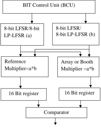
II. BIST ARCHITECTURE
Built-in Test (BIT) is the technique of designing additional hardware and software features into integrated circuits to allow them to perform self-testing, thereby reducing dependence on external automated test equipment (ATE).
Fig 2: BIST Architecture
The components of BIST architecture is given below.
1. Circuit under test : It is the circuit to be tested. It can be either combinational, sequential or memory.
2. Test pattern generator : It generates test patterns for CUT. It is generally a LFSR or ATPG.
3.1Parallel-In-Parallel-Out: It is designed for signature analysis, which is a technique for data compression.
4. Comparator: It compares the value of primary output with the expected output.
5. BIST control unit (BCU): It controls the test execution and manages all the components of a BIST circuit.
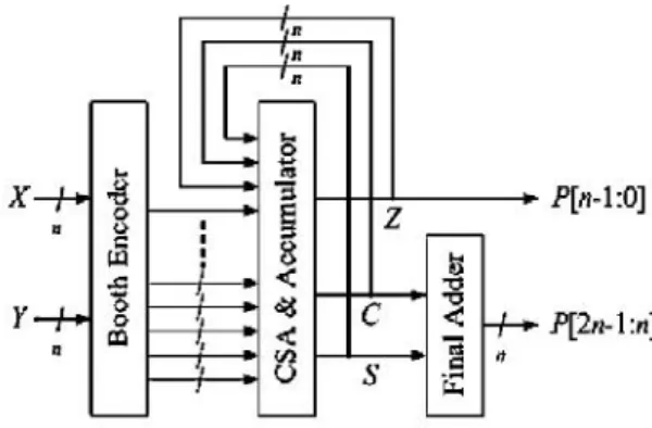
III. MULTIPLIER
Multipliers have large area, long latency and consume considerable power. Reduction of power consumption makes a device reliable. Therefore, low power multipliers with high clock frequencies play an important role in
today’s digital signal processing. Digital signal
processing (DSP) is the technology at the heart of the next generation of personal mobile communication systems. Most DSP systems incorporate a multiplication unit to implement algorithms such as convolution and filtering. Multiplications are basic arithmetic operations used virtually in all applications involving digital signal processing. Multiplication can be considered as a series of repeated additions. Design of portable battery operated multimedia devices requires energy efficient multiplication circuits.
Types of Multiplier
Multipliers are classified by the format in which words are accessed namely:
A. Array Multiplier B. Booth Multiplier
A. Introduction to Array Multiplier: The Fig.3 shows Array Multiplier, in each partial product is generated by taking into account the multiplicand and one bit of multiplier each time. The impending addition is carried out by high-speed carry-save algorithm and the final product is obtained employing any fast adder – the number of partial products depends upon the number of multiplier bits.
Fig 3: Array Multiplier
8-bit LFSR/8-bit
LP-LFSR (a)
Reference
Multiplier=a*b
Array or Booth
Multiplier =a*b
8-bit LFSR/
8-bit LP-LFSR (b)
16 Bit register
16 Bit register
B. Booth Multiplier: The Fig.4 shows the booth multiplier which performs both Signed and Unsigned operations. The main objective of designing the booth multiplier is to perform the partial products to reduce the delay and to increase the speed of the circuit. In this it also reduce the area of the chip used so the power consumption is also reduced in this circuit. The main operation of the booth decoder is to convert the given input to the equivalent booth value. So it contains more number of zeros.
The maximum delay time in the tree type binary multiplying circuit can be determined by the sum of a time in which partial products are formed from the output of the booth decoder having a multiplier provided and a multiplicand, and a time in which the thus formed partial products are added.
Fig 4: Booth Multiplier for Signed and Unsigned operation
By combining the Booth decoders with the partial product generating circuits, the partial products of (m+1) bits should be generated from m multiplicand.
IV. PRIOR WORK
A. Linear Feedback Shift Register (LFSR)
Linear Feedback Shift Register is a circuit consisting of flip-flops connected in series with each other. The output of one flip-flop is connected to the input of the next flip flop and so on. The feedback polynomial which is also known as the characteristic polynomial is used to determine the feedback taps which in turn determines the length of the random pattern generation.
An example below in Fig.5. is used to illustrate the correlation between the LFSR, its characteristic polynomial and matrix theory. In the circuit the feedback taps are shown to be from the output of the 3rd and 1st register.
These taps are indicative of the generator polynomial. Using the matrix theory the companion matrix required for relating the present to the next state is depicted. The actual sequence of the LFSR is represented as BT1, BT2,
BT3…where B is the seed vector. The determinant of the T matrix is called the characteristic polynomial and the generator polynomial is the inverse of the characteristic polynomial.
The increased power consumption by the device in the manufacturing test environment therefore can in most
cases exceed the maximum power consumption specification of the IC resulting in un-repairable device failures begins with a pattern generated using a conventional LFSR causing significant loss of yield. Earlier Techniques for reducing the power dissipation during testing are
1. Another technique was proposed in [3] that is Low transition LFSR for BIST applications. This reduces the average and peak power of circuit during testing.
2. In [4], a Fault model& ATPG algorithm is chosen first, and then test patterns are generated to achieve the desired fault coverage.
3. Proposed a Low power test pattern generation for sequential circuit in [5]. In this paper redundancy is introduced during testing. This will reduces the power consumption without affecting the fault coverage.
Standard LFSR:
Fig 5. 3-bit LFSR Architecture (tap1)
A Linear Feedback Shift Register (LFSR) is a type of pseudorandom number generator. To illustrate an LFSR operation, consider a register that is 3-bits wide.
Start by loading it with an initial seed value. Shift it to the right, and XOR the bit at the output of the last flip-flop and first flip-flip-flop. Then the output of XOR gate is fed to the input of first flip-flop. The seed to be 100 The characteristic polynomial in the general case of an n-bit LFSR to be primitive polynomial it should
• Result in a remainder not equal to 1 for all n≤
L< qn-1
• Remainder of 1 for L= qn-1
Where n=higher order in Characteristic Equation (C.E) Where q =2 (0 or 1)
Here n=3 L= qn-1
For L=3; it result in remainder not equal to 1
For L=4; it result in remainder not equal to 1
For L=5; it result in remainder not equal to 1
For L=6; it result in remainder not equal to 1
Therefore first condition is satisfied i.e remainder not equal to 1 for all n≤ L< qn
-1 i.e L=3,4,5,6.
Therefore second condition is satisfied i.e. remainder equal to 1 for L=7.Therefore P(X)=X3+X +1 is primitive polynomial .
CLK D1 D2 D3
1 1 0 0
2 1 1 0
3 1 1 1
4 0 1 1
5 1 0 1
6 0 1 0
7 0 0 1
8 1 0 0
Table1: Operation of 3-bit LFSR P(X)=X3+X +1
As an another example in fig.6. LFSR operation, consider a register that is 3-bits wide.
P(x)= 1+X+X2+ X3
Fig 6. 3-bit LFSR Architecture(tap1,tap2)
Here n=3 L= qn-1
For L=3; it result in remainder not equal to 1
For L=4; it result in remainder equal to 1
Therefore first condition is not satisfied i.e. remainder equal to 1 for L=4. Thus P(x)= 1+X+X2 + X3 is not a primitive polynomial then it not generates maximum-length sequence i.e. 2N-1.
CLK D1 D2 D3
1 1 0 0
2 1 1 0
3 0 1 1
4 0 0 1
5 1 0 0
Table2: Operation of 3-bit LFSR P(x)= 1+X+X2+ X3
V. PROPOSED METHOD
A. Algorithm for Low Power LFSR (RS-LFSR)
LFSR is a shift register which consists of series of flip flops and is used to generate test patterns for BIST externally. The initial value of LFSR is called seed value. It poses a significant effect on energy consumption [6]. The output that influences the input is called tap. LFSR is
represented by a polynomial known as characteristic polynomial, which is used to determine appropriate feedback taps. A common clock signal is applied to the flip flops which enable the propagation of bits from input to output of flip flops. The correlation between the bits can be achieved by adding more number of test vectors which reduces the switching activity so that the power consumption is reduced.
Fig. 7. Proposed LP LFSR
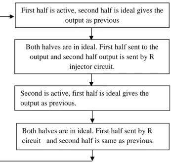
The TPG is activated by two non-overlapping enable signals (en1 and en2). Each enable signal activates one half of the LFSR. In other words, when en1en2=10, first half of the LFSR is active and the second half is in idle mode. The second half is active when en1en2=01. MUX selects either the injection bit or the exact bit in the LFSR.
The proposed approach consists of two half circuits. The algorithm steps says the functions of both half circuits is
Step1: First half is active and second half is idle and gives out is previous; the generating test vector is Ti.
Step2: Both halves are idle First half sent to the output and second half’s output is sent by the injection circuit,
the generating test vector is Ti1.
Step3: Second half is active First half is in idle mode and gives out as previous; the generating test vector is Ti2.
Step4: Both halves are in idle mode, First half is given by injection circuit and Second half is same as previous, the generating test vector is Ti3.
After completing step 4 again goes to step1 for generating test vector Ti+1.
The first level of hierarchy from top to down includes logic circuit design for propagation either the present or next state of flip-flop to second level of hierarchy. Second
Both halves are in ideal. First half sent to the output and second half output is sent by R
injector circuit.
Second is active, first half is ideal gives the output as previous.
Both halves are in ideal. First half sent by R circuit and second half is same as previous. First half is active, second half is ideal gives the
level of hierarchy is implementing Multiplexed (MUX) function i.e. selecting two states to propagate to output which provides more power reduction compared to having only one of the RI injection and Bipartite LFSR techniques in a LFSR due to high randomness of the inserted patterns.
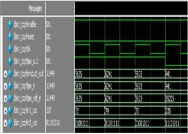
VI. RESULTS
The Model Sim Mentor Graphics EDA tool is used in which conventional and Low Power LFSR is coded in verilog hardware description language. The outputs of Booth Multiplier and Array Multiplier Testing by using Low Power LFSR is Shown in Fig 8.1.and Low power LFSR .
Fig. 8.1. Simulation Result of Booth Multiplier Testing Using LP- LFSR
Fig. 8.2. Simulation Result of Array Multiplier Testing Using LP- LFSR
Module Power(nw) LFSR 7000.436 LP-LFSR 3010.595
Table3: Power LFSR and LP-LFSR
VII.CONCLUSION
For any of the circuit designed, there is need for testing of the circuit. For this purpose, random values are needed, and the random number generator is designed and it generates the random values. BIST is a design for testability (DFT) technique in which testing is carried out using built in hardware features. Since testing is built into the hardware, it is faster and efficient. The proposed test pattern generator reduces the switching activity among the test patterns which is more suitable for Built-In-Self-Test (BIST) structures used for testing of VLSI circuits. Circuits.
REFERENCES
1. B. Chappell, “The Fine Art of IC Design,” IEEE Spectrum, vol. 36, no. 7, July 1999, pp. 30-34.
2. A. Crouch, Design-for-Test for Digital IC’s and
Embedded Core Systems, Prentice Hall, Upper Saddle River, N.J., 1999.
3. Y. Zorian, “A Distributed BIST Control Scheme for Complex VLSI Devices,” Proc. 11th IEEE VLSI Test Symp. (VTS 93), IEEE CS Press, Los Alamitos, Calif., 1993, pp. 4-9.
‘
4. J. Rajski and J. Tyszer, Arithmetic Built-In Self- Test for Embedded Systems, Prentice Hall PTR, Upper Saddle River, N.J., 1998.
5. M.L. Bushnell and V.D. Agrawal, Essentials of Electronic Testing, Kluwer Academic, Boston, 2000, p. 14.
6. S. Wang and S.K. Gupta, “DS-LFSR: A New BIST
TPG for Low Heat Dissipation,” Proc. Int’l Test Conf. (ITC 97), IEEE Press, Piscataway, N.J., 1997, pp. 848-857.
7. J. Monzel et al., “Power Dissipation During Testing: Should We Worry About It?”Proc. 15th IEEE VLSI Test Symp. (VTS 97), IEEE CS Press, Los Alamitos, Calif., 1997, p. 456.
8. T.W. Williams et al., “IDDQ Test: Sensitivity Analysis
of Scaling,” Proc. Int’l Test Conf.(ITC 96), IEEE Press, Piscataway, N.J., 1996, pp. 786-792.
9. M.A. Cirit, “Estimating Dynamic Power Consumption of CMOS Circuits,” Proc. Int’l Conf. Computer-Aided Design (ICCAD 87), IEEE CS Press, Los Alamitos, Calif., 1987, pp. 534-537.
10. C.Y. Wang and K. Roy, “Maximum Power
Estimationfor CMOS Circuits Using Deterministic and
11. N.H.E. Weste, K. Eshraghian, and M.J.S. Smith, Principles of CMOS VLSI Design: A Systems Perspective,Addison-Wesley Longman, Reading,Mass., 2000.
12. A. Krstic, K.T. Cheng, and S.T. Chakradhar, “Testing High Speed VLSI Devices Using Slower Testers,” Proc. 17th VLSI Test Symp. (VTS 99), IEEE CS Press, Los Alamitos, Calif., 1999, pp. 16-21.
13. R. Parkar, “Bare Die Test,”Proc. IEEE Multi-Chip Module Conf., IEEE CS Press, Los Alamitos, Calif., 1992, pp. 24-27.
14. H. Cheung and S. Gupta, “A BIST Methodologyfor Comprehensive Testing of RAM with Reduced Heat
Dissipation,” Proc. Int’l Test Conf.(ITC 96),IEEE Press, Piscataway, N.J., 1996, pp. 22-32.
15. H.J. Wunderlich, “BIST for Systems-on-a-Chip,”
Integration: The VLSI J., vol. 26, nos. 1-2, Dec.n 1998, pp. 55-78.
16. A. Hertwig and H.J. Wunderlich, “Low Power Serial
Built-In Self-Test,” Proc. 3rd European Test Workshop (ETW 98), IEEE CS Press, Los Alamitos, Calif., 1998, pp. 49-53.
17. S. Wang and S.K. Gupta, “ATPG for Heat Dissipation Minimization During Test Application,” IEEE Trans. Computers, vol. 47, no. 2, Feb. 1998, pp.256-262.
18. S. Wang and S.K. Gupta, “ATPG for Heat Dissipation Minimization for Scan Testing,” Proc. 34th ACM/IEEE Design Auto. Conf. (DAC 97), ACM Press, New York, 1997, pp. 614-619.
19. F. Corno et al., “A Test Pattern Generation
Methodology for Low Power Consumption,” Proc. 16th VLSI Test Symp. (VTS 98), IEEE CS Press, Los Alamitos, Calif., 1998, pp 453-459.
20. S. Chakravarty and V. Dabholkar, “Minimizing
Power Dissipation in Scan Circuits During Test
Application,”Proc. IEEE Int’l Workshop on LowPower Design, IEEE CS Press, Los Alamitos, Calif., 1994, pp. 51-56.
21. P. Girard et al., “Reducing Power Consumption during Test Application by Test Vector Ordering,” Proc.
Int’l Symp. Circuits and Systems (ISCAS 98), Part II, IEEE CS Press, Los Alamitos, Calif., 1998, pp. 296-299.
22. P. Girard et al., “A Test Vector Ordering Technique for Switching Activity Reduction during TestOperation,”
Proc. 9th Great Lakes Symp. on VLSI(GLS-VLSI 99), IEEE CS Press, Los Alamitos,Calif., 1999, pp. 24-27.
23. V. Dabholkar et al., “Techniques for ReducingPower Dissipation During Test Application in Full Scan
Circuits,”IEEE Trans. Computer-Aided Design, vol. 17, no. 12, Dec. 1998, pp. 1325-1333.
24. Y. Bonhomme et al., “Scan Cell Ordering for Low
Power Scan Testing,” to be published in Proc. 7th European Test Workshop (ETW 02), IEEE CS Press, Los Alamitos, Calif., 2002.
25. T.C. Huang and K.J. Lee, “An Input Control
Techniquefor Power Reduction in Scan Circuits During Test Application,”Proc. 8th Asian Test Symp. (ATS 99), IEEE CS Press, Los Alamitos, Calif.,
P. SAI KUMAR currently pursuing his M.Tech in VLSI
DESIGN from AKULA GOPPAYYA COLLEGE OF ENGG, Prathipadu, West Godavari, India affiliated to JNTU Kakinada, he has done his B.Tech degree from Sri Vasavi College of Engg., affiliated to JNTU Kakinada, Tadepalligudem, West Godavari district, India and his fields of interest include VLSI and Digital electronics.
N.S.GOVIND working as Asst. Professor and Head of