Sharif University of Technology
Scientia IranicaTransactions D: Computer Science & Engineering and Electrical Engineering www.scientiairanica.com
Research Note
An analysis on the main formulas of Z-source inverter
M. Shid Pilehvar, M. Mardaneh
and A. Rajaei
Department of Electrical and Electronics Engineering, Shiraz University of Technology, Shiraz, Iran. Received 7 November 2013; received in revised form 15 December 2014; accepted 13 April 2015
KEYWORDS Z-source inverter; Voltage stress; Current ripple; Switching loss; Switching device power.
Abstract. This paper proposes an analysis of the calculation of voltage and current ripples, voltage stresses, switching device power, and switching loss in the Z-source inverter. In this paper, the formulas of the inductor current ripple, capacitor voltage ripple, voltage stress on the devices and capacitors, switching device power and switching loss, are presented. Computing these formulas will help us greatly in the performance improvement of the Z-source inverter, and in this paper, a detailed analysis of the main formulas is presented. Simulation results are also given to conrm the analysis.
c
2015 Sharif University of Technology. All rights reserved.
1. Introduction
The Voltage Source Inverter (VSI) and the Current Source Inverter (CSI) are two traditional types of inverter. For the VSI, a dc voltage source paralleled with a large capacitor feeds a three-phase bridge (consisting of six switches). This dc voltage source can be a battery, fuel cell or solar cell. For the CSI, a dc current source feeds a three-phase bridge (consisting of six switches). This dc current source can be a large inductor which is fed from a battery, fuel cell or solar cell. Despite widespread use, these two traditional inverters have problems. For example, for the VSI, the ac output voltage is lower than the input dc voltage, thus, it can only perform a buck dc-ac power conversion. On the other hand, for the CSI, the ac output voltage is greater than the input dc voltage, thus, presenting a voltage boost dc-ac power conversion. Therefore, in applications where both voltage buck and boost are needed, an additional dc-dc converter should be placed before both VSI and CSI, which signicantly increases the complexity and cost of the system. To overcome this problem, and many
*. Corresponding author. Tel.: +98 71 37264121; Fax: +98 71 37353502
E-mail address: mardaneh@sutech.ac.ir (M. Mardaneh)
other problems of traditional inverters, in 2002, the topology of the Z-source inverter [1] was proposed by Peng.
Unlike other inverters, the Z-source inverter can provide shoot-through states to boost the input dc voltage when both switches in the same phase leg are on, and, because of this feature, the reliability of the inverter is greatly improved. In comparison to traditional inverters, the Z-source inverter is more reliable, has lower costs and higher eciency [2].
In recent years, the Z-source inverter has received wide attention in research and industrial applications, including motor drives [3], photovoltaic systems [4,5] and the traction drive of fuel cell-battery hybrid electric vehicles [6]. Besides, some investigations have also presented new methods for performance improvement of the Z-source inverter, such as reduction of Z-source capacitor voltage stress [7], minimization of induc-tor current ripple [8,9], and improvement of voltage boost ability [10]. In this paper, an analysis of the main formulas of the Z-source inverter is pro-posed. For this purpose, the formulas of the induc-tor current ripple, capaciinduc-tor voltage ripple, voltage stress on the devices and capacitors, switching device power and switching loss, are calculated. Simula-tion results are also presented to validate the analy-sis.
Figure 1. Conguration of Z-source inverter.
2. Operation principle of Z-source inverter Figure 1 shows the structure of the Z-source inverter. The Z-source inverter operates in two modes: the shoot-through state and non-shoot-through state. In the shoot-through state, both switches of the same phase leg are on, simultaneously, and, in a non-shoot-through state, the upper switch of a phase leg and the lower switch of another phase leg are connected, simultaneously.
As analyzed in [1], If the capacitors and inductors of the Z-source impedance network have the same capacitance and inductance (C1 = C2 = C and L1 =
L2 = L), respectively, the maximum value of the
Z-source impedance output voltage can be calculated as follows:
^vi= VC vL= 2VC Vdc= TTsw
1 T0Vdc= BVdc;(1)
where B is the boost factor and can be obtained as follows:
B = Tsw T1 T0 =
1
1 2(T0=Tsw) =
1
1 2D 1; (2) where T0 and T1 are the total shoot-through state
and total non-shoot-through state times, respectively, during one switching cycle, Tsw, and Tsw = T0+ T1. It
should be noted that D is the shoot-through duty ratio, which is greater than, or equal to, zero, and less than, or equal to, 0.5, and can be obtained from T0=Tsw.
The peak value of the fundamental output phase voltage can be expressed as:
(^vo)1= M ^v2 i: (3)
According to Eq. (1), Eq. (3) can be further expressed as:
(^vo)1= MBV2 dc: (4)
To control the Z-source inverter, all traditional pulsewidth modulations (PWM) can be used. But, when the dc source voltage is not large enough, a modied PWM with shoot-through states is needed to increase the voltage [1]. Figure 2 shows the
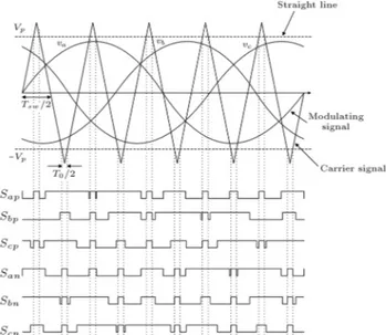
Figure 2. Waveforms and switching strategy of PWM control method for Z-source inverter, considering shoot-through states.
proposed PWM for the Z-source inverter used in this study.
In this investigation, to control the shoot-through duty ratio and produce switching PWM pulses, a triangular carrier signal is compared with a sinusoidal modulating signal. Also, two straight lines are used as shoot-through reference lines, Vp and Vp. As
shown in Figure 2, whenever the triangular waveform is more than Vpor less than Vp, the Z-source inverter
operates in a shoot-through state. It should be noted that Vp is equal or greater than the peak value of the
modulating signals, and, in this study, the frequency of the modulating signals is taken as 60 Hz.
3. Voltage stresses
3.1. Z-source capacitor voltage stress
As analyzed in [1], the capacitor voltage of the Z-source impedance network can be calculated as follows:
VC1 = VC2= VC=
1 T0=Tsw
1 2T0=Tsw
Vdc
=1 2D1 D Vdc: (5)
From Eqs. (2) and (5), the Z-source capacitor voltage can be further expressed as:
Vc =B + 12B BVdc= B + 12 Vdc: (6)
Therefore, from Eq. (6), VC increases by enhancing B
or Vdc.
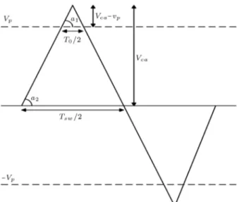
As shown in Figure 3, the boost factor can be controlled by the values of straight lines, as follows:
Figure 3. Triangular carrier signal and two straight lines in one switching cycle.
tan a1=VcaT Vp
0=4 ; (7)
and:
tan a2=TVca
sw=4; (8)
where Vca is the peak value of the triangular carrier
signal.
According to Figure 3, since angle a1 is equal
to angle a2, the shoot-through duty ratio can be
calculated from Eqs. (7) and (8), as shown below: T0
Tsw =
Vca Vp
Vca = D: (9)
By substituting Eq. (9) into Eq. (2), the boost factor can be expressed as:
B = 1
1 2Vca Vp
Vca
: (10)
According to Eqs. (9) and (10), when Vca is constant
and Vp is increased, D and B are reduced. In such
circumstances, from Eq. (6), VC will decrease.
The Z-source capacitor voltage can be considered as the voltage stress across the capacitors, SC, and,
from Eqs. (6) and (10), it can be further determined by the following relation:
SC= Vc= 2V Vp
p VcaVdc: (11)
As can be derived from Eq. (11), Vpcannot be less than
Vca=2. Also, if Vp= Vca=2, VC goes to innity, then, a
high Z-source capacitor voltage stress is presented.
3.2. Voltage stress across the devices
According to Eq. (1), the voltage stress across the switches, SS, can be expressed as:
SS = ^vi= BVdc: (12)
From Eqs. (2) and (12), it can be concluded that: SS = 1
1 2Vca Vp
Vca
Vdc= 2VVca
p VcaVdc: (13)
As can be derived from Eq. (13), SS increases by
enhancing Vdc and decreases by enhancing Vp. Also,
if Vp = Vca=2, SS goes to innity, this may damage
the switching devices, because of the limitation of their voltage rating.
4. Current and voltage ripples 4.1. Z-source inductor current ripple
As previously mentioned, during the shoot-through state, the inductors are charged by the capacitors. Therefore, the Z-source inductor current ripple can be expressed as:
iL=T0LVC = DTswLVC: (14)
From Eqs. (2), (6) and (14), it can be concluded that: iL=B
2 1
4B
TswVdc
L : (15)
As can be derived from Eq. (15), iL increases by
enhancing Tsw or Vdc and decreases by enhancing L.
Also, if B = 1 or D = 0, iL is equal to zero.
By substituting Eq. (10) into Eq. (15), the Z-source inductor current ripple can be further expressed as:
iL= VcaVp V 2 p
Vca(2Vp Vca)
TswVdc
L : (16)
From Eq. (16), it can be concluded that changing Vp
has a signicant impact on iL, so, if Vp = Vca=2 or
D = 0:5, then, iL goes to innity.
4.2. Z-source capacitor voltage ripple
As previously mentioned, during the shoot-through state, capacitors are discharged by the Z-source induc-tor current. Therefore, the voltage ripple across the capacitors can be expressed as:
VC= T0CIL =DTCswIL: (17)
By applying the steady-state analysis presented in [11], the average values of the Z-source inductor current and
load current can be obtained as follows:
IL= 1 2D1 D Il; (18)
Il= VRC
l: (19)
From Eqs. (18) and (19), it can be concluded that: VC= D(1 D)1 2D TswCIl = D(1 D)1 2D TCRswVC
l : (20)
Substituting Eq. (19) into Eq. (20) gives the following relation;
VC= D
1 D 1 2D
2T swVdc
CRl : (21)
According to Eq. (2), Eq. (21) can be further expressed as:
Vc= (B + 1)(B 2 1)
8B
TswVdc
CRl : (22)
As can be derived from Eq. (22), VC increases by
enhancing Tsw or Vdc, and decreases by enhancing C.
Also, if B = 1 or D = 0, then, VC is equal to zero.
By substituting Eq. (10) into Eq. (22), the Z-source capacitor voltage ripple can be further expressed as:
Vc= Vp(VpVca V 2 p)
Vca(2Vp Vca)2
TswVdc
CRl : (23)
From Eq. (23), it can be concluded that changing Vp
has a signicant impact on VC. Also, if Vp = Vca=2
or D = 0:5, then VC goes to innity.
5. Total switching device power
Each switching device of the Z-source inverter should be selected according to the peak and average current impressed and the maximum voltage on it. For this purpose, the Switching Device Power (SDP) for each switch is introduced. The total SDP of the Z-source inverter is equal to the sum of SDP of all the switching devices used in the circuit. Actually, total SDP is a measure to choose the appropriate semiconductor devices, and thus, an important cost indicator of the Z-source inverter, whose average and peak are given by:
Total average SDP = (SDP)t= n
X
k=1
^vskisk; (24a)
Total peak SDP = ( ^SDP)t= n
X
k=1
^vsk^isk; (24b)
where n is the number of switching devices used in the
circuit. Also, isk and bisk are the average and peak
current through the kth switch, and ^vsk is the peak
voltage impressing the kth switch.
As previously mentioned, the current to the in-verter bridge, ii, consists of two elements. One is
the current to the load during the non-shoot-through state and the other is the current through the switches during the shoot-through state. The current through the inverter during the shoot-through state is 2iL, and,
because of the symmetry of the circuit, this current is evenly distributed in three parallel paths. Therefore, the average current through each switch of the inverter bridge during the shoot-through state can be expressed as:
Iss= 2i3L =2I3L: (25)
The peak fundamental output line current of the Z-source inverter can be calculated as:
(^io)1= 3(^v2Po
o)1cos '; (26)
where Pois the output power of the Z-source inverter.
Also, it is assumed that the load current of phase a is lagging by ' from its load voltage.
In the non-shoot-through state, from Eqs. (17) and (26), and since the line current is evenly shared by two switches in a line cycle, the average current through each switch is the same as conventional PWM inverters, and can be expressed as:
Isn=22 (^io)1=3(^v2Po o)1cos '=
4Po
3MBVdccos ':(27)
From Eqs. (25) and (27), the average current through each switch of the inverter bridge can be obtained as follows:
Is= IssTT0 sw + Isn
1 TT0
sw
=23ILD +3MBV4Po
dccos '(1 D): (28)
From Eqs. (1), (24) and (28), the total average switching device power of the Z-source inverter can be calculated as follows:
SDPt=6^viIs=1 2D4D ILVdc+(1 D)M cos '8Po :
(29) According to Eqs. (2) and (29), it can be concluded that:
SDPt= 2(B 1)ILVdc+(B + 1)2B M cos '8Po : (30)
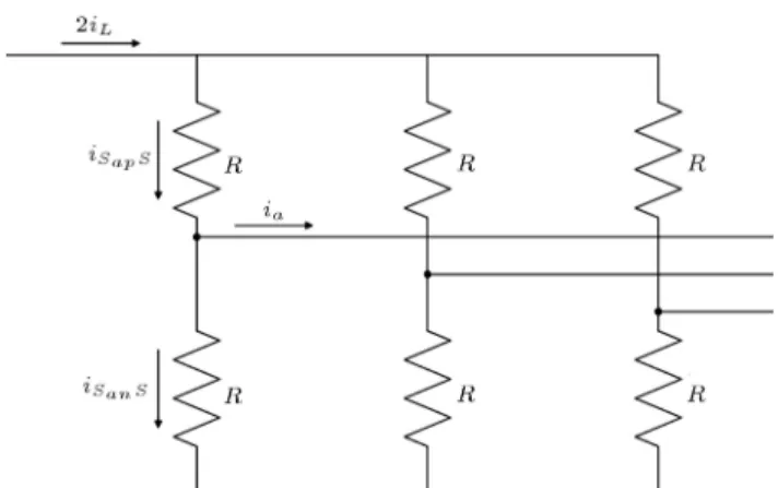
Figure 4. Model of the inverter bridge during shoot-through state.
average switching device power of the Z-source inverter can be further expressed as:
SDPt=4V(2Vp2(Vca Vp)
p Vca)3
V2 dc
Rl +
Vp
Vca
8Po
M cos ': (31) To calculate the ( ^SDP)t, both peak currents through
the switches during shoot-through and non-shoot-through states are needed. As shown in Figure 4, if all switches have the same resistance during the shoot-through state, it can be concluded that:
^iSaps=
1 2ia+
2
3iL: (32)
By ignoring the Z-source inductor current ripple, when ia is at its peak, the peak current through switch Sap
occurs, which can be obtained as follows: ^iSaps=
1 2^ia+
2 3IL=
1 2(^io)1+
2
3IL: (33) According to Eqs. (16), (26) and (33), the peak current through switch Sapduring the shoot-through state can
be further determined by the following relation: ^iSaps=
Po
3(^vo)1cos '+
2 3IL=
2Po
3MBVdccos '+
2 3IL:(34) Therefore, from Eqs. (1) and (34), the total peak switching device power of the Z-source inverter during the shoot-through state can be calculated as follows:
( ^SDP)ts= 6^vi^iSaps=
4Po
3M cos '+ 4BILVdc: (35) From Eqs. (18), (19) and (35), the total peak switching device power of the Z-source inverter during the shoot-through state can be further expressed as:
( ^SDP)ts= 3M cos '4Po + B(B + 1)2V 2 dc
Rl
= 3M cos '4Po +(2V4VcaVp2
p Vca)3
V2 dc
Rl: (36)
On the other hand, the peak current through the
switching devices during the non-shoot-through state is equal to the peak fundamental output line current of the Z-source inverter, and can be obtained as follows:
^iSapn= (^io)1=
2Po
3(^vo)1cos ': (37)
Therefore, from Eqs. (1), (17), and (37), the total peak switching device power of the Z-source inverter during the non-shoot-through state can be calculated as follows:
( ^SDP)tn= 6^vi^iSapn =
8Po
M cos ': (38) According to Eqs. (36) and (38), the total peak switching device power of the Z-source inverter can be expressed as:
( ^SDP)t= max
^ SDP
ts; ( ^SDP)tn
=max 4Po 3M cos '+
4VcaVp2
(2Vp Vca)3
V2 dc
Rl;
8Po
M cos ' !
: (39) The average input current from the dc source, Iin,
is equal to the average current through the Z-source inductor, IL. Therefore, by ignoring the total loss of
the Z-source inverter, the input power from the dc source, Pin, is equal to the output power, Po, and it
can be concluded that: Iin= IL= VPo
dc: (40)
By substituting Eq. (40) into Eqs. (29) and (35), the total average and peak switching device powers of the Z-source inverter can be approximately calculated as follows:
(SDP)t4(V2Vca Vp) p Vca Po+
Vp
Vca
8Po
M cos '; (41) ( ^SDP)tmax
4Po
3M cos '+ 4Vca
2Vp VcaPo;
8Po
M cos '
: (42) From Eqs. (41) and (42), the total average and peak Switching Device Power Ratios (SDPR) of the Z-source inverter can be expressed as:
(SDPR)av=(SDP)P t o =
4(Vca Vp)
2Vp Vca +
Vp
Vca
8
M cos ';(43) (SDPR)pk= ( ^SDP)P t
o
=max
4 3M cos '+
4Vca
2Vp Vca;
8 M cos '
: (44) As can be derived from Eqs. (43) and (44), a change in parameters, such as Vp, M and ', has a signicant
6. Switching loss
Although high values of switching frequency, fsw, cause
low voltage and current ripples, they also increase the switching loss of the Z-source inverter. The switching loss of each IGBT during non-through and shoot-through states, Pswnand Psws, are given by [2]:
Pswn=2T1
sw(Eswonn+ Eswon)
0 B @
Z
0
sin xdx 12
5 6Z ' 6 '
jsin xj dx 1 C
A ; (45)
Psws= 2T1
sw(Eswons+ Eswos); (46)
where Eswonn and Eswon are the turn on and turn o
energy loss of the IGBT at peak current, respectively. Also, Eswons and Eswos are the turn on and turn o
energy losses corresponding to the average switching current of the shoot-through state, which is 2iL=3.
The Switching Loss Ratio (SLR) for a three-phase Z-source inverter can be obtained as follows:
SLR =SLRn+ SLRs= E Pswn swonn+ Eswon
+E Psws
swons+ Eswos; (47)
where SLRn and SLRs are the switching loss ratio
of each IGBT during non-through and shoot-through states, respectively.
Therefore, by substituting Eqs. (45) and (46) into Eq. (47), the switching loss ratio can be further expressed as:
SLR=2T1
sw
0 B @1+1
0 B @
Z
0
sin xdx 12
5 6 '
Z
6 '
jsin xj dx 1 C A 1 C A :
(48) As can be derived from Eq. (48), a change in param-eters, such as Tsw and ', has a signicant impact on
SLR.
7. Simulation results
In this section, simulation results are given to conrm the proposed analysis of the main formulas of the source inverter. For this purpose, a three-phase Z-source inverter is studied, whose constant parameters are listed in Table 1.
Figure 5(a) and (b) show the voltage stresses across the Z-source capacitor and switching devices, respectively. In these gures, it can be seen that SC and SS are approximately boosted to 342 V and
Table 1. List of constant parameters and their values. Parameter Value Parameter Value
Vdc (V) 150 Vca 1
Rl() 30 Vp 0.64
L (H) 16010 6 M 0.64
C (F) 100010 6 Tsw (s) 9:8310 5
' (rad) 6:6610 5 fsw(Hz) 10:17103
Figure 5. Simulated waveforms of voltage stresses across the (a) Z-source capacitor, and (b) switching devices.
Figure 6. Simulated waveforms of the (a) Z-source inductor current, (b) Z-source average inductor current, and (c) Z-source inductor current with details.
536 V, respectively. These two values are quite close to theoretical values.
Figure 6 shows the Z-source inductor current iL
and its average value, IL. As indicated by this gure,
IL is approximately equal to 25 A, perfectly close to
Figure 7. Simulated waveforms of the (a) Z-source capacitor voltage, (b) Z-source average capacitor voltage, and (c) Z-source capacitor voltage with details.
Figure 8. Simulated waveforms of the (a) output phase current, and (b) output phase voltage, for the Z-source inverter.
As indicated by the simulation results in Figure 7, the voltage ripple across the capacitors is very low, and, therefore, the Z-source capacitor voltage, VC, and its
average value, VCav, are quite close to each other. On
the other hand, VCav is boosted to 341 V, perfectly
matching the theoretical value.
Figure 8(a) and (b) show the ltered output phase current and voltage of the Z-source inverter, ioand vo,
respectively. It is clear that io and vo are perfectly
consistent with theoretical values. 8. Conclusion
In this paper, an analysis on the calculation of the main formulas of a Z-source inverter has been proposed. The
formulas of the inductor current ripple, capacitor volt-age ripple, voltvolt-age stress on the devices and capacitors, switching device power and switching loss have been computed. Calculating these formulas will greatly help in improving the performance of the Z-source inverter. Simulation results have also been presented which are perfectly consistent with theoretical values, and this compatibility between theoretical and simulation results has validated the analysis.
References
1. Peng, F.Z. \Z-source inverter", IEEE Transactions on Industry Applications, 39(2), pp. 504-510 (2003).
2. Shen, M., Joseph, A., Wang, J., Peng, F.Z. et al. \Comparison of traditional inverters and Z-source inverter for fuel cell vehicles", IEEE Transactions on Power Electronics, 22(4), pp. 1453-1463 (2007).
3. Peng, F.Z., Joseph, A., Wang, J., Shen, M. et al. \Z-source inverter for motor drives", IEEE Transactions on Power Electronics, 20(4), pp. 857-863 (2005).
4. Hanif, M., Basu, M. and Gaughan, K. \Understanding the operation of a Z-source inverter for photovoltaic application with a design example", IET Power Elec-tronics, 4(3), pp. 278-287 (2011).
5. Bradaschia, F., Cavalcanti, M.C., Ferraz, P.E., Neves, F.A. et al. \Modulation for three-phase transformerless Z-source inverter to reduce leakage currents in pho-tovoltaic systems", IEEE Transactions on Industrial Electronics, 58(12), pp. 5385-5395 (2011).
6. Peng, F.Z., Shen, M. and Holland, K. \Application of Z-source inverter for traction drive of fuel cell-battery hybrid electric vehicles", IEEE Transactions on Power Electronics, 22(3), pp. 1054-1061 (2007).
7. Tang, Y., Xie, S., Zhang, C. and Xu, Z. \Improved Z-source inverter with reduced Z-Z-source capacitor volt-age stress and soft-start capability", IEEE Transac-tions on Power Electronics, 24(2), pp. 409-415 (2009).
8. Shen, M., Wang, J., Joseph, A., Peng, F.Z. et al. \Constant boost control of the Z-source inverter to minimize current ripple and voltage stress", IEEE Transactions on Industry Applications, 42(3), pp. 770-778 (2006).
9. Tang, Y., Xie, S. and Ding, J. \Pulse width modulation of Z-source inverters with minimum inductor current ripple", IEEE Transactions on Industrial Electronics, 61(1), pp. 98-106 (2014).
10. Peng, F.Z., Shen, M. and Qian, Z. \Maximum boost control of the Z-source inverter", IEEE Transactions on Power Electronics, 20(4), pp. 833-838 (2005).
11. Liu, J., Hu, J. and Xu, L. \Dynamic modeling and analysis of z source converter-derivation of Ac small signal model and design-oriented analysis", IEEE Transactions on Power Electronics, 22(5), pp. 1786-1796 (2007).
Biographies
Mohsen Shid Pilehvar received a BS degree in Electrical Engineering from Ferdowsi University, Mash-had, Iran, in 2011, and an MS degree in the same subject from Shiraz University of Technology, Shiraz, Iran, in 2013. His research interests include power electronics, Z-source inverter, multilevel inverters, and application of power electronics in renewable energy systems.
Mohammad Mardaneh received a BS degree in Electrical Engineering from Shiraz University, Iran, in 2002, and MS and PhD degrees in the same subject from Amirkabir University of Technology, Tehran,
Iran, in 2004 and 2008, respectively. He has been Assistant Professor at Shiraz University of Technology, Shiraz, Iran, since 2008. His research interests include modeling, design and control of electrical machines and application of power electronics in renewable energy systems and distribution networks.
Amirhossein Rajaei was born in Jahrom, Iran. He received MS and PhD degrees in Electrical Engineering from Tarbiat Modares University, Tehran, Iran, in 2009 and 2013, respectively. He is currently Assistant Professor at Shiraz University of Technology, Shiraz, Iran. His main research interests include renewable energy resources, power converters, electric vehicles, and motor drive systems.