2016 International Conference on Mathematical, Computational and Statistical Sciences and Engineering (MCSSE 2016) ISBN: 978-1-60595-396-0
Design and Realisation of DDR2 SDRAM Controller for
Image Real-time Processing Based on FPGA
Si-min GUAN, Fan-liang BU
*and Guang-di LIU
People’s Public Security University of China, Tuanhe Campus, Huangyi Road, Daxing District, Beijing City, China
*Corresponding author
Keywords: FPGA, DDR2 SDRAM, Verilog HDL, Quartus II.
Abstract. According to the needs of real-time cache, high-rate storage and reading data of image processing system, this paper designs a kind of DDR2 SDRAM controller and introduces the system architecture and data channel of DDR2 controller. The function module of DDR2 controller is designed by using Verilog HDL through the modular design pattern. Then the function of each module and the configuration of core IP are described in detail. Finally, the simulation result of DDR2 controller proves that it can be well applied to the image processing system based on FPGA.
Introduction
The real-time buffer of image data is the most basic work in the system of real-time image enhancement and display based on FPGA (Field Programmable Gate Array). As the clock frequency of each unit in the system is different, there is a need for a memory controller to exchange data between each unit. Because the chip memory is completed within the FPGA and the circuit board parts without any other external links, so the Chip memory storage is the most practical memory in the embedded system based on FPGA, which is through the Avalon interface to read/write and data transmission between the FPGA each logic[1].The top-level module design and each sub module required functionality is completed by Verilog HDL (Hardware Description Language) and based on the modular design thought, it takes the Quartus II 13.1 as the design platform and designs it through a top-down approach. Finally, simulation experiments were performed, and this design is implemented on Cyclone IV EP4CE22F17C8N of Altera.
Principle of DDR2 SDRAM Controller
SDRAM (Synchronous Dynamic Random-Access Memory) is one of the many types of RAM, the synchronisation means that SDRAM needs to rely on the clock to coordinate the work and its internal instruction sending, data transmission need to clock synchronisation as a benchmark. SDRAM experienced DDR SDRAM (Double Data Rate) and DDR2 SDRAM stage and now has developed to the DDR3 SDRAM phase. But DDR3 is more suitable for the advanced processing system and the cost is more expensive, in contrast, DDR2 storage capacity and read speed is more suitable for embedded systems.
DDR2 and DDR have the same data collection methods that are to perform data transmission at the same time on the rising edge and the falling edge of the clock. But DDR2 has a lot of improvement in performance compared to DDR, Table 1 lists the main differences between them[2].
Table 1. The Difference Between DDR and DDR2.
Item DDR DDR2
Bus Frequency 100/133/166/200[MHz] 200/266/333[MHz]
Core Frequency 100/133/166/200[MHz] 100/133/166[MHz]
Data-Transter Frequency 200/266/333/400[MHz] 400/533/667[MHz]
Pre-Read 2[bit] 4[bit]
Burst Length 2,4,8 4,8
Number Of Bank <=4 <=8
CAS Delay 1.5,2,2.5 3,4,5
DQS Single Data Selection Pulse Differential Data Selection Pulse
Working Voltage 2.5[V] 1.8[V]
Package TSOP FBGA
Heat High Low
Module Design of DDR2 SDRAM Controller
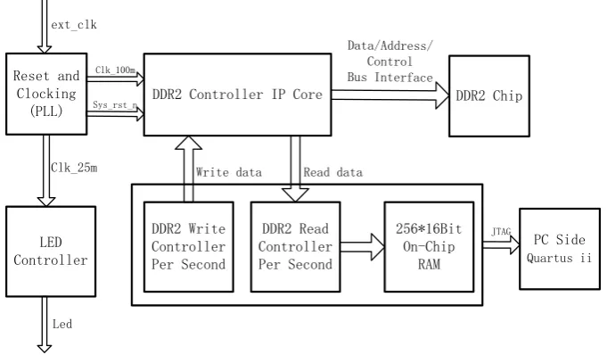
In this paper, the top-level module gsm_DDR2 of DDR2 SDRAM module is designed by using a top-down design model[3], which includes six sub modules as shown in Figure 1.
Reset and Clocking
(PLL)
DDR2 Controller IP Core
LED Controller DDR2 Chip DDR2 Write Controller Per Second DDR2 Read Controller Per Second 256*16Bit On-Chip RAM PC Side Quartus ii
Write data Read data
[image:2.595.127.468.310.509.2]Data/Address/ Control Bus Interface JTAG Clk_25m Clk_100m Sys_rst_n ext_clk Led
Figure 1. Schematic diagram of module.
The top-level module don't do anything about logical processing but it only serves as a connecting channel for all sub-modules, as well as to define the connection interface of external FPGA and Chip DDR2. The design of the six sub-modules are: sld_hub module, ddr2_controller module, onchipram_for_ddr module, led_controller module, PLL module and a data_source module that is used to generate the experimental data.
The sld_hub module that is a VHDL (Very-High-Speed Hardware Description Language) file is used as a protocol channel for data exchange between Quartus II and RAM in FPGA based on JTAG debug communication interface. The sld_hub module can be automatically generated through the configuration of RAM IP soft core. Quartus II only allows users to use the sld_hub module that is depicted with Very-High-Speed Hardware Description Language, but users don’t know what source code is, which as a black box for the user.
The ddr2_controller module is developed for initiation, reset delay and generates the corresponding control signals and the instructions of read, write, receive and respond, which can be used to achieve the DDR2 state transition and time sequence synchronisation and other functions. The ddr2_controller module is an IP soft core too. The onchipram_for_ddr module is used to partition a RAM space within FPGA.
and 100MHz, are generated by the PLL (Phase Locking Loop ) module that could only have 25MHz to provide the clock signal frequency that is required by all the modules.
[image:3.595.172.423.171.322.2]The data_source module that is simulation data generation module is designed for generate a set of continuous regular data periodically and then write into the 0-1023 address in DDR2. Simultaneously, this module can read the data from the 0-1023 address of the DDR2 regularly to write in chip RAM of FPGA, which in order to verify the effectiveness of read and write operation of the entire DDR2 SDRAM controller. Figure 2 is the RTL view of the entire module.
Figure 2. RTL Viewer of gsm_DDR2 module.
Configuration of DDR2 SDRAM Controller and Simulation of FPGA Data
IP Core Configuration of DDR2 Controller
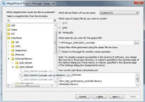
IP core (Intellectual Property core) is a kind of logic or chip design module that can be reused and has been verified by experiments, which can greatly shorten the design cycle and simplify the design process. Specific configuration methods are as follows:
[image:3.595.176.418.535.705.2](1) Firstly, open the project, you can choose the ‘MegaWizard Plug-In Manager’ option in the Tool button from the menu bar, then the ‘Create a new custom megafunction variation’ option. Under the ‘Select a megafunction from the list below’ option, we found the needed IP core 'SDRAM Controller with ALTMEMPHY v13.1 DDR2', named ‘ddr2_controller’. The created file type is selected as Verilog HDL and the device family selection Cyclone IV E as shown below in Figure 3 and clicks the Next button.
Figure 3. Find ‘DDR2 SDRAM Controller with ALTMEMPHY v13.1’ from the list of ‘Select a megafunction from the list below’.
Select Micron MT47H32M16CC-3 in the Micron Memory Presets list. Next select ‘Modify parameters... ‘button and then change the value of ‘Memory burst length’ to 8 in ‘Preset Editor’, which avoids the error brought by choice the ‘Half’ mode in ‘Controller data rate’ option when generating the IP core. Finally, click on next as shown below in Figure 4.
Figure 4. DDR2 IP core configuration interface.
(3) The other settings are the default value of the system and the last step to click the Finish button.So far the DDR2 SDRAM controller IP core what we need is completed.
Data Simulation and Experimental Results
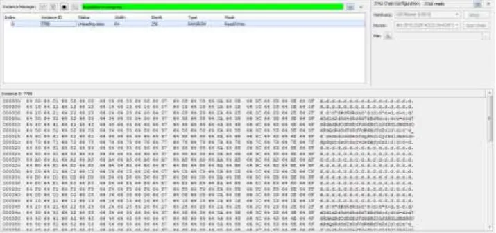
In this paper, the Cyclone EP4CE22F17C8 IV of Altera is used to verify the function of the DDR2 SDRAM controller. At first, the program is downloaded to the experimental board and run the program, click the Memory button in the Index to read the data from the experiment when the indicator light on the test board is blinking, as Figure 5 illustrates.
Figure 5. Real-time readout of data from the experimental board.
As you can see from the data has been read, the high byte data is added once a second in all 16 bit and the low byte data is added with the increase of address from 00, but the low byte of data does not change with the increase of time. And as can be seen from the experimental results, the data we read and the data generated by the data_source module are consistent, its function and time sequence meet the design requirements.
Conclusions
[image:4.595.120.478.427.595.2]FPGA successfully. Hence, the research production of this thesis is valuable for both theory reference and practical application.
References
[1] Altera Corporation. DDR & DDR2 SDRAM Controller Compiler User Guide. Altera Corporation, April 2005.
[2] JEDEC.JESD79-2F DDR2 SDRAM Specification[S], JEDEC Solid State Technology Assocition, 2009.