2017 2nd International Conference on Computer Science and Technology (CST 2017) ISBN: 978-1-60595-461-5
Standard Cell Library Characterization of 28nm
Process Based on Machine Learning
Yi-qi SHE
1, Li-jun ZHANG
2, a,* Jian-bin ZHENG
3, Ai-lin ZHANG
4,
Yue-ping ZHU
5and You-zhong LI
61, 2School of Urban Rail Transportation, Soochow University, Suzhou, China 215000
3, 4, 5Megacores Technology Co., LTD., Suzhou, China 215000
6School of Urban Rail Transportation, Soochow University, Suzhou, China 215000
*Corresponding author
Keywords: Standard cell library, Machine learning, Linear regression.
Abstract. This article presents a new learning method based on machine learning, which can quickly and accurately draw up the characterization of the Static Random-Access Memory (SRAM) compiler and standard cell library. The timing of 10 standard circuits with different process corners and their key parameters were collected. According to the 10-fold cross validation, the regression model was established by linear regression. After comparing the influence of different parameters on path delay, determination coefficient of training set and testing set were 0.979 and 0.955, respectively. Relative Error of training set and test set were 0.9458 and 0.8736, respectively. Then, the timing of a D type flip-flop (DFF) was selected as the target of the regression. At the same time, the determination coefficients of the regression model training set and the testing set are 0.9992 and 0.9992, respectively. Relative Error of training set and test set were 0.9882 and 0.9868, respectively. The results show that the model fitted the timing of DFF by the path delay of other circuits is better than the previous method.
Introduction
Since Dynamic Voltage and Frequency Scaling (DVFS) was introduced into System on Chip (SOC), SOC worked under hundreds of megabytes clock frequency. Similarly, SRAM, as an important part of SOC, needed to work under the same clock frequency [1]. A SRAM compiler has thousands of instances, for one instance, it’s simulation in different process variations must be implemented to achieve characterization.
DVFS makes the SOC design voltage nodes for signoff increase a lot. In the case of 28nm low power, standard working voltage is 1.1v, which corresponds to 6 corners need signoff. The median voltage range is from 0.7v to 1.2v, taking each 50mv as a node, a total of 66 corners requires signoff [2]. Namely, it means that there must be 66 corners of memory and standard cell library characterization.
Standard Cell Library Simulation
[image:2.612.115.494.156.452.2]In semiconductor design, standard cell methodology is a method of designing application specific integrated circuits (ASICs) with mostly digital-logic features. Considered that time cost of SRAM compiler, we used standard cell library of 28nm process to make a test, and 10 circuits of standard cell library are INV, AND2, AND3, NOR2B, NOR2, AOI211, XOR3, ADDF, DFFNQ, DFFNSRPQ.
Table 1. 325 Sets of process corners. Process FNFP SNSP TNTP FNSP SNFP
[image:2.612.227.365.354.428.2]Voltage [V] 0.84 0.875 0.91 0.945 0.98 1.015 1.05 1.085 1.12 1.155 1.19 1.225 1.26 Temperature [°C] -40 0 25 85 125
[image:2.612.206.379.476.545.2]Figure 1. DFF functional schematic.
Figure 2. Path delay: from input 50% transition to output low 10% transition.
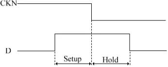
Figure 3. Setup time and fold time of DFF.
All simulation used H-Spice which based on Bsim4 spice model, and slew is set to 1ns. Path delay is the time from the input pin to the output pin. Take DFFs as an example, as shown in Fig. 1 and Fig. 2, pin D is input terminal while pin Q is output terminal. Path delay sets from input 50% transition to output high 90% transition or from input 50% transition to output low 10% transition to make sure output pin has already achieved goal electric potential. Fig. 3 illustrates that setup time means the time required for data to remain stable until the clock arrives, and hold time means the time required for data to remain stable after the clock arrives. Setup time was the time of signal from pin D to node ‘m’, and hold time were the time of signal from node ‘m’ to node ‘s’ and the time of signal from pin D to node ‘nm’, and the bigger one was selected as the true hold time [3].
Linear Regression
In the practical application, circuits can run stably, the corresponding simulation result has no outlier. There are small differences in the parameters of each group, but the difference between groups was large, namely, there is no multicollinearity between features. Taking the above factors and more than one feature into account, we choose multiple linear regression to solve the regression problem.
(1)
Eq. 1 fits a linear model with coefficients = ( ) and features to minimize the residual sum of squares between the observed responses in the dataset, and the response predicted by the linear approximation. The value of coefficients will not be known, and it must be estimated from sample data. Classical least squares regression consists of minimizing the sum of the squared residuals [4, 5].
(2)
In Eq. 2, means the value predicted by linear model, and means the real value of target, there are many methods to obtain the minimum value of : least squares and gradient descent. Batch gradient descent need to iterate through all the data at every iteration, so batch gradient descent only suits for small data. Stochastic gradient descent doesn`t need traverse all of the data, it can only get close to the minimum value rather than the true minimum value. Least square is a very intuitive algorithm which calculates the minimum value by matrix operations. Cost function gets the minimum value when
Method of Circuit Parameters
In this article, our purpose is to explain some detail of the extracting technique, the main features of the relationships hidden or implied in the tabulated figures. Nevertheless, the study of regression analysis techniques will also provide certain insights into how to plan the collection of data [6, 7].
MOSFET is a four-terminal device, and the four terminals are called drain (D), gate (G), source (S), and body (B) [8]. Each terminal affects the function of MOS, MOSFET and it`s logical structure affects the function of circuits. So we select some parameters of MOS transistor and circuits as machine learning`s features, and path delay as machine learning`s target. According to [8], [9], [10], [11], we set some parameters of MOS in Table 2:
Table 2. Some parameters of MOS transistor. Ivin [A] The peak current of drive voltage when the signal flipping Ivdd [A] The peak current of pin VDD when the signal flipping Ivss [A] The peak current of pin VSS when the signal flipping
Ion [A] The average current of MOS transistors after the signal flipped Ipeak [A] The peak current of MOS transistors when the signal flipping Vth [V] The threshold voltage of MOS transistors when the signal flipping
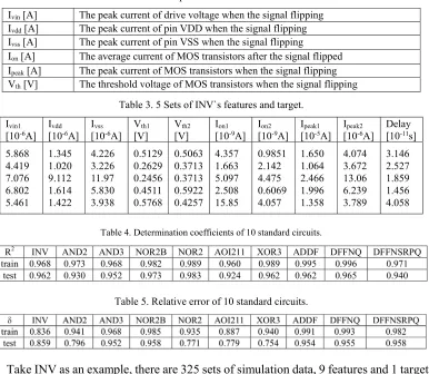
Table 3. 5 Sets of INV`s features and target. Ivin1
[10-6A] Ivdd [10-6A] [10Ivss -6A] Vth1 [V] Vth2 [V] Ion1 [10-9A] Ion2 [10-9A] Ipeak1 [10-5A] Ipeak2 [10-6A] Delay [10-11s] 5.868 4.419 7.076 6.802 5.461 1.345 1.020 9.112 1.614 1.422 4.226 3.226 11.97 5.830 3.938 0.5129 0.2629 0.2456 0.4511 0.5768 0.5063 0.3713 0.3713 0.5922 0.4257 4.357 1.663 5.097 2.508 15.85 0.9851 2.142 4.475 0.6069 4.057 1.650 1.064 2.466 1.996 1.358 4.074 3.672 13.06 6.239 3.789 3.146 2.527 1.859 1.456 4.058
Table 4. Determination coefficients of 10 standard circuits.
Table 5. Relative error of 10 standard circuits.
Take INV as an example, there are 325 sets of simulation data, 9 features and 1 target in each set. There are 5 sets of INV`s features and targets in Table 3. The regression model uses 10-fold cross validation to obtain more accurate results [12]. As shown in Table 4 and Table 5, there were determination coefficients and relative error of training set and testing set in each circuits` regression [13]. By the definition of parameter, R2 is very close to 1, which means that the regression fitting degree is very good, δ is also very close to 1, which means that the predicted timing is very accuracy.
Some circuits have many parameters of circuits, especially some parameters related to MOS transistors, such as Ion, Ipeak, Vth, all MOS transistors have these parameters. There will be quite a few of circuit`s parameters which make regression more complex. Method of Path Delay
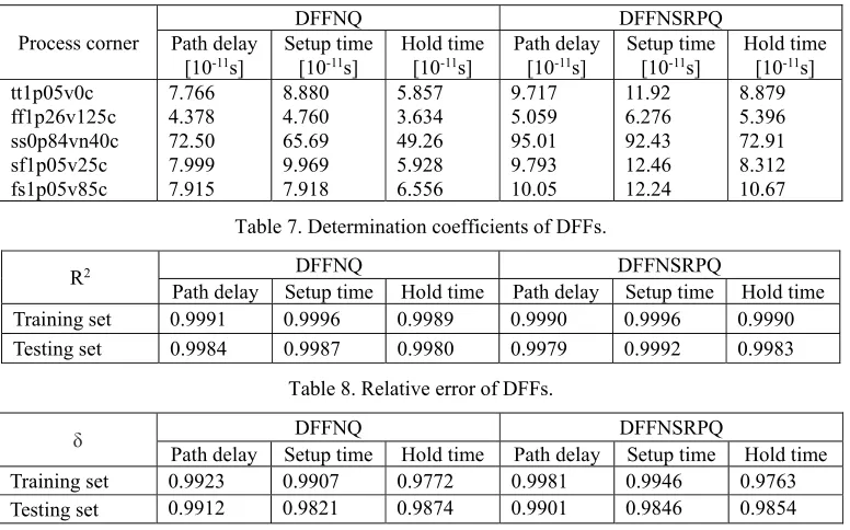
The regression model also uses 10-fold cross validation to obtain more accurate results. Table 7 lists determination coefficients of DFFs training set and testing set, Table 8 lists relative error of DFFs training set and testing set. By the definition of parameter, R2 is especially close to 1, which means that the regression fitting degree is quite good, δ is also especially close to 1, which means that the predicted timing is quite accuracy. Comparing with the previous method, this method uses less feature, and the fitting effect is very good.
Table 6. Timing of DFFs in 5 process corners.
Process corner
DFFNQ DFFNSRPQ
Path delay
[image:5.612.114.502.180.422.2][10-11s] Setup time [10-11s] Hold time [10-11s] Path delay [10-11s] Setup time [10-11s] Hold time [10-11s] tt1p05v0c ff1p26v125c ss0p84vn40c sf1p05v25c fs1p05v85c 7.766 4.378 72.50 7.999 7.915 8.880 4.760 65.69 9.969 7.918 5.857 3.634 49.26 5.928 6.556 9.717 5.059 95.01 9.793 10.05 11.92 6.276 92.43 12.46 12.24 8.879 5.396 72.91 8.312 10.67 Table 7. Determination coefficients of DFFs.
R2 DFFNQ DFFNSRPQ
Path delay Setup time Hold time Path delay Setup time Hold time Training set 0.9991 0.9996 0.9989 0.9990 0.9996 0.9990 Testing set 0.9984 0.9987 0.9980 0.9979 0.9992 0.9983
Table 8. Relative error of DFFs.
δ DFFNQ DFFNSRPQ
Path delay Setup time Hold time Path delay Setup time Hold time Training set 0.9923 0.9907 0.9772 0.9981 0.9946 0.9763 Testing set 0.9912 0.9821 0.9874 0.9901 0.9846 0.9854
Conclusions
Based on the standard cell library as an example, this article attempted to propose two methods to predict timing. The previous method used parameters of circuits as features and timing as target, and the last method used timing of circuits as features and timing of DFFs as target. The results showed both of them can achieved good results. Method of timing fitted better and predicted target more accurately. From this point of view, it is feasible to predict timing by linear regression, which also provides a feasible idea to predict timing of SRAM compiler.
Acknowledgement
This work is supported by National Natural Science Foundation of China, and the Foundation Numbers are No.61272105, and No.61076102.
This work also supported by the Opening Project of Key Laboratory of Microelectronic Devices & Integrated Technology, Institute of Microelectronics, Chinese Academy of Sciences.
References
[2] Fu, H. Timing Signoff Uncertainty for UDSM SoC Design[C] International Conference on Asic, 2003. Proceedings. IEEE Xplore, 2003:113-117 Vol.1.
[3] Övünç, Polat, Manzak, A. Design and analysis of low power Carbon Nanotube Field Effect Transistor (CNFET) D Flip-Flops (DFFs)[C] International Conference on Computer Research and Development. IEEE, 2011:399-401.
[4] Montgomery, D. C., Peck, E. A., Vining, G. G. Introduction to linear regression analysis. 4th ed [J]. Technometrics, 1983, 25(4).
[5] Rousseeuw, P. J. Least Median of Squares Regression [J]. Journal of the American Statistical Association, 1984, 79(388):871-880.
[6] Zhou, Zhihua. Machine learning [M] In Chinese. Tsinghua University press, 2016. [7] Edition S. Applied Linear Regression Models[J]. Technometrics, 2016(3).
[8] Cheng, Y., Hu, C. Mosfet Modeling & BSIM3 User’s Guide [J]. 1999.
[9] Liu, W., Hu, C. BSIM4 and MOSFET modeling for IC simulation [M]. World Scientific, 2011.
[10] Miuramattausch, M, Mattausch, H. J., Ezaki, T. The Physics and Modeling of Mosfets[M]. WORLD SCIENTIFIC, 2017.
[11] Liu, Z. H., Hu, C., Huang, J. H., et al. Threshold voltage model for deep-submicrometer MOSFETs [J]. IEEE Transactions on Electron Devices, 1993, 40(1):86-95.
[12] Zhang, Y., Yang, Y. Cross-validation for selecting a model selection procedure[J]. Journal of Econometrics, 2015, 187(1):95-112.