Effect of Electrical Defloration in Liquid and Solid
Crystals
Valentin. A. Tsvetkov
Problem Laboratory of Moscow State Academy of the Instruments Engineering and Computer Sciences, Moscow, Russia. Email: [email protected]
Received February 16th,2013; revised March 16th, 2013; accepted March 24th, 2013
Copyright © 2013 Valentin. A. Tsvetkov. This is an open access article distributed under the Creative Commons Attribution License, which permits unrestricted use, distribution, and reproduction in any medium, provided the original work is properly cited.
ABSTRACT
Earlier we observed a movement of the front of ions in the bulk of an ordered LC sample across which the driven volt- age was applied [1]. This movement looked as waving zigzag curvatures in the pattern of interference strips. It was shown that behind the movable front of ions, the LC volume was getting charged. The author has found out that, in his pioneer experiments made in 1974, he observed the similar electrooptical phenomena on a single crystal of niobate- strontium-barium (NBS). Just after applying driving voltage (in a crossed electrical field crystal sample geometry) a system of curved interference strips is arising, which is evolving for the time period of about ten minutes at the driven voltage being kept constant. The evolution of the interference stripes pattern near positive, negative electrodes and in middle part of sample occurs in some different ways. At the end of evolution the system of strips disappears and the sample becomes practically homogeneous. The described process can be observed only once at the first applying of the driving voltage. This process is caused by redistribution of charges frozen at the crystallization and which are having an opportunity of the recombination at the first applying of the driving voltage. The obtained results are discussed with the possible applying the given experimental technique for solid and LCs parameters studying.
Keywords: LC; Carrier; Volumetric Charge; Ferroelectric Solid Crystal
1. Introduction
During some time we were engaged in studing move- ment of charged carriers in ordered bulk samples of nematic liquid crystals (LC). The LC sample was placed in a parallelepiped-shape cavity of a size of 3 × 8 × 0.3 mm. The internal walls of the cavity (except two lateral sides) were rubbed in a horizontal direction for providing planar orientation. The lateral sides were covered with thin film copper electrodes that were processed for provi- ding homeotropic orientation.
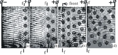
[image:1.595.310.539.594.701.2]At the coordinated aligning action of all of the sides a rather perfect monocrystal texture was created in the parallelepiped volume, with monocrystal optical axis being directed in the horizontal direction. In the absence of driving voltage the texture of LC sample, observed at crossed polarizes, looked like a system of horizontal interference’s strips, stipulated by variations in thickness
Figure 1. When the driving voltage (for example, 60 V d.c.) was applied to the LC sample, waving zigzag curvatures in the pattern of interference strips were induced near the positive electrode, the front of which
moved to the negative one with the velocity of about 6
m/sec.
We have shown that the LC volume behind the waving front has a surplus volumetric charge, whereas the LC volume before the waving front was electrically neutral. After the waving front passes through the whole sample, all LC volume is getting volumetric charged. Under the driving voltage applied the sample texture looked like waving zigzag curvatures in the pattern of interference
strips. These phenomena are the result of local distortions of the external electrical field and of hydrodynamical stream flows both caused by moveable (driven) ions.
After the driving voltage is switched off, the curved interference strips are straightened and for the period of time of ~1.5 - 2 hours (optical relaxation time) they acquire an appearance of initial (undisturbed) inter- ference pattern. The volumetric charge relaxes during neutral. After the waving front passes through the whole sample, all LC volume is getting volumetric charged. Under the driving voltage applied the sample texture looked like waving zigzag curvatures in the pattern of interference strips. These phenomena are the result of local distortions of the external electrical field and of hydrodynamical stream flows both caused by moveable (driven) ions.
After the driving voltage is switched off, the curved interference strips are straightened and for the period of time of ~1.5 - 2 hours (optical relaxation time) they acquire an appearance of initial (undisturbed) inter- ference pattern. The volumetric charge relaxes during 10 - 12 hours (the charge relaxation time).
The described above processes can be repeated un- limited number of times provided that the volumetric charge is allowed completely to relax (i.e. the experi-
ments may be repeated in the period of time not less than 12 hours).
The present work was carried out in the Microelec- tronics Department of Radio & Electronics Institute (RAS), where the electrooptical properties of the solid ferroelectric monocrystal of noibat-barium-stroncium (NBS) were being studied by the neighboring team. So, we had decided to repeat the described above experi- ments with the sample of NBS-crystal.
2. Investigations of Solid Crystals
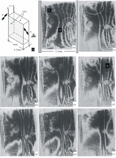
The sample represented a parallelepiped of a size of 1.5 × 5 × 15 mm with the optical axis being directed along the side of 1.5 mm Figure 2(а). All sides of the sample were carefully polished. On the lateral sides of the sample the metal electrodes (chromium) were deposited.
1) In the initial state being observed at crossed polar- izes along the 5mm-size side, the sample had an appear ance of a homogeneous clear field. At applying 150 V d.c. to lateral sides (cross electric field mode of operation) interference strips were appeared in the optical pattern of the sample, indicating the presence of the electrooptical response for the inspected crystal. As the applied voltage changed the number of interference strips and their local- ization were essentially changed too. After the voltage switched-off the strips were disappeared and the sample pattern acquired an appearance of that at the initial state. Thus, the common cross electrooptical effect was ob-
served.
2) We have found out that the electrooptical effect shows to some extent difference dependent upon whether the voltage is applied for the first time or it is done for the next ones. This difference consists of that at the first voltage applying there is a certain system of interference strips, which evolves for a long time. The various phases of this evolution are given in Figures 2(b)-(i). Just after the driving voltage applied, a system of narrow inter- ference strips arises near the left (negative) electrode
Figure 2(b) (area L).
In the other part of the sample (except area D) a system of relatively wide curved strips arises with the axis of total structure parallel to electrodes. In area D, apparently, there is a large defect of the crystal lattice not visible before applying the electric field. This defect distorting the local electric field is visualized just after the electric field is applied. After some time Figure 2(c)
the strips in L-area are getting a little bit wider and their number is decreased. In the other sample part the number of strips are decreased, as well and they become smooth including the D-area
3. Discussion
Figure 2. Sketch of sample and successive frames of evolution of interferencion strips. (a): sketch of sample; (b): 5 min after applying 50 V d.c.; (c (d, e, f, g, h, i)): 10 (20, 35, 45, 55, > 60) min after applying 50 V d.c.
uniformity of the local electric field and its value chang- ing at the constant external electric field applied is un- equal in value current caused by non-uniform distribution of carriers in different parts of the sample.
Let’s consider the equivalent electrical circuit of the
sample (one pipe of a current) as a circuit in series con- nected resistances RL, Rm1, Rm2, RR. The resistances RL,
RR characterize, accordingly, the left (negative) and the
of the sample. A current in the dielectrics, though also very small, is caused by carriers, which might be, in principal, free electrons, holes, drifting through the de- fects of the ionic crystal lattice, and in ferroelectrical crystals there are also charge carriers captured by domain boundaries.
During the process of monocrystal growth from a crystallizing crystal melt, an ordered crystal lattice is formed. The main problem of the monocrystal growth is the correct distribution of ions in the points of crystal lattice with possibly minimal number of failures. The problem of the local electrical neutrality for the formed lattice is not any way controlled and is solely a sponta- neous process. It is rather probable, that to the moment of formation of following crystal layers there is a surplus or lack of electrons in some crystal lattice points of the pre- vious layers and this charges distribution appears to be frozen in a grown crystal sample.Thus, in a crystal bulk chaotically located centers can exist (and does exist, as this is experimentally proved), that capture an excess (overbalance) of electrons or/and holes .The carriers can also be accumulated near the borders of domains of a ferroelectrical crystal, what the NBS sample studied ac- tually is. And, in different parts of the sample there can simultaneously exist an excess of both free electrons and holes that are not recombine with each other because of significant distances between places of their localization.
If an external electric field is applied to such a ferro- electric crystal (represented electrically a conglomerate of domains and defects with chaotically distributed free charges), then electrons will begin to be injected from the negative electrode into the crystal bulk. One portion of the injected electrons will recombine with the hole ex- cess in the L-area just adjacent to the negative electrode, the other one forms a bulk overbalanced negative charge in the same near-electrode L-area.
2) Near the positive electrode a depletion region of electrons is formed, as some overbalanced electrons are rejected into the positive electrode, and others can re- combine with moveable free electrons, which can move from the middle crystal layers to the positive electrode area when the external electric field is applied.
As in the initial state the distribution of carriers over the crystal bulk is non-uniform, the resistance magnitude of Rm1, Rm2, RR for equidistant parts (from electrodes) of
the sampleare different. It results in different potentials for equidistant sample points and, as consequence, dif- ferent optical phase shift along the equidistant sample lines. That’s why the interference strips are bent.
3) In initial state, in the middle part of the sample there are charged carriers non-recombined by different reasons. After applying the electric field the free charged carriers begin to move: electrons are moving to the positive elec- trode, holes are moving to the negative electrode. During
this counterpart carriers movement some of them may recombine that can not be done before the electric field applying. As a result, the amount of the electrical non- homogeneities in the middle part of the sample is de- creased and crystal bulk is getting more homogeneous electrically. In any case the resistance distribution pattern of the crystal volume is changed. Thisleads to theredis- tribution of the electric potentials in the sample volume in accordance with the new resistance values of RL, Rm1,
Rm2, RR. As the result of the potential redistribution in the
sample bulk, new interference strip patterns arise, which are presented in the all-subsequent photos Figures 2(c)- (i). The described above processes last during the long period of time because of very small magnitudes of mo- bility of charged carriers that take place in a good insu- lator the NBS-crystal really is.
4) In boundary areas, especially in the L-layer adjacent to the negative electrode, under the electric field applied, there is an area having the pattern of plenty of narrow interference strips weakly changing with time. It is clear that free electrons exceedingly saturate this area and such a state is very stable. That’s why, the interference strip pattern near the electrodes is small unchangeable in time.
In the R-area, near the positive electrode, for the all period of the electric field applied there is also a system of interference strips, which wider than those near the negative electrode, and the whole system itself is greatly wider than that in the L-area, near the negative electro- de.
After the long period of time most of the carriers in the middle part of the sample recombine and the electric field is getting practically homogeneous. The interferen- ce pattern of Figure 2(i) corresponds to this state.
5) After the electric field is switched off, the interfere- ence pattern in the middle of the sample is disappeared in a fraction of second, for the negative electrode area it takes several minutes, and for the positive electrode area it lasts more than several days. The last circumstance is due to the difficulties of volume charge relaxation that takes place in a good dielectric with very low carrier mo- bility. Even for the poor dielectric, what LC is, the vol- ume charge relaxation time is about of 10 - 12 hours for sample geometry close to described one [1].
changeable. It confirms the fact that at the first applica- tion of the external electric field there occurred an ire- versible change of the electrical condition in the volume of the sample.
By analogy to beautiful process, known in an alive nature it is possible to name the observed electrooptical phenomena as “electrical defloration”.
7) The mobility of carriers in LCs is rather large for the sample to relax to the initial state completely even if the relaxation process lasted for long time. In solid crys- tals the mobility of carriers is small. Therefore, up to the first driving electric field application to a crystal sample, chaotically dispersed over the crystal bulk carriers had no chance to recombine, except the couples for which carri- ers were very close to each other. But after switching-on and durable action of an external electric field, additional numbers of carrier couples have chances to recombine, that’s why the sample volume is getting more homoge- neous electrically. This energetic state is a stable one and there is no reason to return to the original state.
8) Owing to grate difference in carrier mobilities for LC’s and solid crystals, electrical defloration process in LC’s can be repeated an unlimited number of times. On the contrary, for solid crystals it is fundamentally a non- recurring phenomenon that can occur only one time.
9) A usage of the carrier transport observation tech- nique in LC’s for solid electrooptical crystals allowed us to observe and explain the new electrooptical phenome- non for the last (named by us as “electrical defloration”). Besides, as it’s seen in Figure 2(b) (area D), it is possi- ble to observe process of homogenization of charges in the field of defects. In Figure 2(i) one can see, that at the end of defloration process there were left only small traces from originally existing large area D. It opens an opportunity for the further development of described technique for visualization and nondestructive inspection of defects in solid single crystals.
10) Another interesting phenomenon observed with the described technique is a formation of system of fine parallel interference strips which have a width size of about 40 m. They are directed at the angle ~45˚ to the verticals in area М during time from 5 mines up to 240 of mines Figures 2(b)-(i). Unfortunately, these strips are well seen only in the original photos or at the large opti- cal increase.
It is quite possible, that here we observe a process of formation of monodomain ferroelectrical crystal (by the way, as far as we know, nobody observed domains in NBS as early as we had done).
At the beginning of the process one can not observe any stripes. It explains our first failure we had in our very early attempts to visualize expected domain structure for NBS-crystal by depositing onto the polished crystal sur- face or onto the crystal chip a thin LC-layer. It is the
same technique, which allowed visualizing domains, for example, in triglycine sulfate-crystal (TGS) [2]. That time we had not seen any attributes of domain structure in NBS. And a conclusion was made that the domains are too small and outside the technique limit. Under the elec- tric field applied, the domains, fine, invisible by any other techniques, with different directions of polarization, are polarized and form larger domains (recrystalization and monodomainization processes). Then, after some period of time of d.c. electric field action, they became visible Figures 2(с)-(е).
At the further reorganization process, the monodomain structure is practically formed.
We have paid attention to these fine strips in photos only at writing this paper and now we have no chance to repeat the experiment. Therefore, the interpretation of these strips as domain existing is one of the possible hy- potheses not forbidden by nature, but also not confirm- ed precisely the domain existing. If those are domains, their sizes in the initial condition would be less than 40
m and then, it is logical, that we could not to visualize them by putting onto the chip surface a LC layer of smaller thickness (~20 - 30 m) than domains were of.
4. Conclusions
1) The experimental technique of observing electric field distortions induced by the moving charged carriers in a LC-medium under the constant electric field was used for studying the charged carrier movement in a solid ferroelectric crystal of niobate-strontium-barium. There are given the comparison of processes of transportation of charges carriers in LCs and solid crystal in close ge-ometries of experiment. The analogies and distinctions of these processes are shown.
2) A noncontradicting-to-physical-laws explanation of electroptical phenomena arising near the anode, the cathode and in the middle part of the NBS-crystal sample is given on the basis of experimental studying the evolu- tion of the interference pattern induced by the external electric field applied to the sample. In particular, single process of homogenization of electric nonhomogeneities formed in process of ferroelectric crystal growth was shown to occur in the middle part of the crystal sample.
It is obvious that at a lot of experiences with identical on thickness and for each experience by new (fresh) samples it ispossible to receive the quantitative informa- tion on mobility of carriers in a solid crystal.
3) With the described technique there were observed processes of homogenization of electric near-defect non- homogeneities. In future the technique can be advanced for the quality control of electrooptical crystals.
abiity. In the initial state they are of a size less than 40
m.
5. Acknowledgements
The author wish to thank Drs Zakharov L. and Ermakova (Phillipova) O. (Laboratory of Microelectronics of RAS) for the delivered NBS-sample and fruitful discussion, in spite of the fact that not on all questions we had identical opinion.
REFERENCES
[1] V. A Tsvetkov and O. V. Tsvetkov, “Ions Influence on Electrooptical Characteristics of NLC”. Molecular Crys- tals and Liquid Crystals, Vol. 368, No. 1, 2001, pp. 625- 632.doi:10.1080/10587250108029995
[2] N. A. Tikhomirova, S. A. Pikin, et al., “Vizualization of
domains in ferroelectricTGS crystals,” Ferroelectrics, 29,