Failure analysis using I
DD
current leakage and
photo localization for gate oxide defect of CMOS
VLSI
Farisal Abdullah1, 2, Nafarizal Nayan1, Muhammad Mahadi Abdul Jamil1 1
Faculty of Electrical and Electronic Engineering,
University Tun Hussein Onn Malaysia. 2
Department of Product Failure Analysis Engineering,
ST Microelectronics Sdn Bhd – Muar, Malaysia. Email: [email protected]
Abstract— The typical electrical degradation on the
complementary metal oxide semiconductor (CMOS) performance is due to defect in gate oxide layer. During integrated circuit (IC) infant mortality phase, stress tests introduced at wafer sort and final test in order to assured only good IC being deliver to end customer. Stress tests such as burn-in, gate stress, and quiescent current (IDDQ) test, demonstrated their competency to screen out this type of early failure. Nevertheless, the latent defect is a time dependent failure, which, affect the CMOS reliability after certain time, temperatures and application stress. Consequently, revise failure analysis technique has to be introduced in effective approach to compensate the problem in the current technology due to metal interconnection layers and dense for front side failure analysis (FA). The motivation of this work is to present the fault localization on the elevated IDD current of the faulty logic cells during the transition by photo localization technique and clarify gate oxide defect through circuit simulation. We have confirmed that the IDD scan test and photo localization technique were effective to localize faulty IC in silicon active area through front side.
Keywords-component; CMOS VLSI;silicon dioxid;, failure analysis;IDD scan; fault localization.
I. INTRODUCTION
The slim layer of a SiO2 is a non-crystalline and amorphous material, which were used to isolate the transistor gate from its channel. Nowadays, automotive product application such as Bipolar CMOS DMOS (BCD) technology is known as a typical kind of Application Specific Integrated Circuit (ASIC) device which capable to operate analog, digital and power function inside the same chip for automotive product application, i.e. Air-Bag, Automatic Brake System
(ABS), Electric Power Steering (EPS) and etc. In the earlier BCD 1 technology era, the gate oxide thickness is about 300Å (30nm), then decreasing progressively to 70Å (7nm) for BCD 9 [1]. Figure 1 graphically illustrates the trend of gate oxide thickness towards technology and the applied voltages.
The reduction of gate oxide thickness was resulted due to the technology scaling demand. However, it becomes major concern on oxide quality and reliability. Thinner oxide denotes to increase the driver current controlled and short channel effects and at the same time, it may potentially fail earlier than the product warranty given by the IC manufacturer.
Fig.1: The BCD technology trend on oxide thickness, gate length and applied voltage [1].
bcd1 bcd2 bcd3 bcd4 bcd5 bcd6 bcd8 bcd9 0.0
200.0n 400.0n 600.0n 800.0n 1.0µ 1.2µ
1.2v 1.8v 3.3v
2010 gateL GOXthickness
BCD Technologies
g
a
te
l
e
n
g
th
Downscalling CMOS dimension on BCD Technology
1988
Vdd=5v MOS Voltage
5.0n 10.0n 15.0n 20.0n 25.0n 30.0n
S
iO
2
th
ic
k
n
e
s
s
70Å/120nm 300Å/1µm
Source: STM-APG Products
Proceedings of 2010 IEEE Student Conference on Research and Development (SCOReD 2010), 13 - 14 Dec 2010, Putrajaya, Malaysia
II. MODEL SiO2DEFECT.
Fig.2: SiO2 molecules bond geometry orientation, cited from [3].
Generally, silicon dioxide (SiO2) layer made during the wafer diffusion process in the chemical ratio of silicon (Si) to oxygen (O) atoms. From molecular orientation as shows on Figure 2, Si atom emerge to bond four O atoms with each O atom also bond to another Si atom. The SiO2 tetrahedron molecules are inflexible with formation of about 109° angles between Si and O bond. Notable from this rigid bonding, the bond angles form is about 120° to 180°, with mean of 150° [2]. Hence, diverging angle from its mean value will turn the bond angle to become weak and then finally resulting in faulty condition. This inconsistent bond strength becomes the foundation of statistical conduct for the oxide wear-off and breakdown for current research and development in this field.
In today's electronic circuit miniaturization and complexity requirement, the ultra thin oxide with <30Å thickness has challenged the quality and reliability concern [3]. From the design for application point of view, the CMOS voltage has been downgrading as well as the channel length (L) in order to introduce IC with more high speed and at the same time less power consumption. From this emerging, leakage current can be less by minimizing the trapped electron charge inside the oxide layer. However, for nano-metric CMOS Very Large Scale Integrated (VLSI) circuit requirement, as the oxide layer became thinner, it compensate by quantum tunneling effect which amplifies exponentially in leading the gate to channel current leakage [4].
Fig.3 (a): CMOS structure in three-dimension form and the expected current leakage (by arrow).
In the present study, we will investigate the gate oxide defect on BCD. First, we will simulate the defect model using OrCAD simulation and then we will localize the defect using emission
microscope. Figure 3(a) and (b) shows the physical model of Ohmic short between the gate and the terminals for drain, source, and channel, which may possibly occur during the breakdown or wear out phase [5]. These models will be use during the OrCAD simulation
III. DEFECT SIMULATION ON OXIDE.
amps Rfault
Vss Vdd
Ifault = ( − ) (1)
[image:2.612.55.217.64.220.2]Theoretically, elevated IDD can measure based on the magnitude of Rfault [6]. The calculation shown by equation (1) was derives from the typical Ohms Law, which represent the amount of leakage current flow during the logic transition.
Fig.4: The ohmic short model affected by the p-Ch. M1 cell by using OrCAD simulation for IDD current examines.
The equivalent OR logic shown in Figure 6 were designed with 0.6µm CMOS technology by Cadence ORCAD software. The circuit designed with embedded Ohmic defect, proposed from the gate oxide short (GOS) models. During the simulation, 1 kHz of CLK speeds and 5V of VDD supply MOS voltage were used, considered as the most suitable frequency and voltage work for this technology. Study on the leakage current via simulation also performed on the fault free circuit for the sake of comparison.
The Ohmic defect in Figure 4 circuit, p-ch MOS of OR cell assured that it does not modify the logic state of the output. However, results shown in Table 1 & 2 demonstrated that irregular IDD current were elevated, and causes high power consumption on the circuit which in reality working IC, it will wear-out as a killer defect. The proposed value is to illustrate as a latent defect, which presented during the infant phase. It may weaken during the stress test and applicative condition; subsequently break down during the normal life.
Research and study earlier on the Ohmic value proposed with a few kΩ. It has shows how the oxide
breakdown experiments by using electrostatic discharge Si
Oxygen
Ө=109º Ө=120º~180º
Si
Oxygen
p-substrate
n-well
p+ n+
Thin oxide Gate
[image:2.612.329.552.226.399.2] [image:2.612.74.280.541.602.2](ESD) and laser techniques contributed with a great amount of leakage current can be detected [7].
Hence, few Ohmic values can only emphasize to indicate the gate oxide failure during the early phase of the IC for Design for Testability (DfT) development.
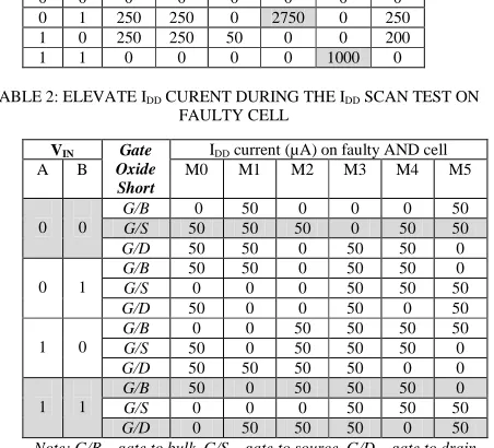
TABLE 1: ELEVATE IDD CURENT DURING THE IDD SCAN TEST ON
FAULT-FREE CELL
VIN IDD current (µA) on fault-free AND cell
A B M0 M1 M2 M3 M4 M5
0 0 0 0 0 0 0 0
0 1 250 250 0 2750 0 250
1 0 250 250 50 0 0 200
[image:3.612.72.298.179.384.2]1 1 0 0 0 0 1000 0
TABLE 2: ELEVATE IDD CURENT DURING THE IDD SCAN TEST ON
FAULTY CELL
VIN Gate Oxide Short
IDD current (µA) on faulty AND cell
A B M0 M1 M2 M3 M4
M5
0 0
G/B 0 50 0 0 0 50
G/S 50 50 50 0 50 50
G/D 50 50 0 50 50 0
0 1
G/B 50 50 0 50 50 0
G/S 0 0 0 50 50 50
G/D 50 0 0 50 0 50
1 0
G/B 0 0 50 50 50 50
G/S 50 0 50 50 50 0
G/D 50 50 50 50 0 0
1 1
G/B 50 0 50 50 50 0
G/S 0 0 0 50 50 50
G/D 0 50 50 50 0 50
Note: G/B – gate to bulk, G/S – gate to source, G/D – gate to drain
[image:3.612.68.544.433.654.2]Based on the measured leakage current during the simulation, the simplified test pattern as an output which can be used to sensitize the current inside the circuit with ‘00’ and ‘11’ input patterns, as highlighted in grey color on the table. Both patterns were sufficient to cover these three GOS models, which were introduce into the circuit earlier.
Fig.5: Comparable elevated IDD between faulty circuit and fault free.
Even through the fault circuit measured with lower current than the fault-free circuit, Figure 5 shows the current for the fault free circuit (M2) rise in a pulse, ranging from picoseconds to nanosecond time. On the other hand, the current for the faulty circuit consequence from the Ohmic defect R1, rise in mill-seconds. For fault localization technique using photo emission, the rising time effect will reflect how much proton will be emitted from the working CMOS due to the collective emission time by the failure analysis (FA) tool.
Therefore, exposing the circuit with longer elevated IDD time may benefit the defect to be sensitized and localized. For the fault localization techniques, it can be estimate based on the equipment sensitivity. The broad requirement on the nano -electronics failure analysis shows the recommendation of several types of equipments. The fundamental of selective appropriate equipments for failure analysis is really depending on the detector and leakage current sensitivity versus with the spatial resolution of defect size estimation [8].
IV.FAULT LOCALIZATION METHOD
Fault localization on the faulty IC with 0.8µm technology has been analyzed with front-side failure analysis. An emission microscope (EMMI) of Hamamatsu PHEMOS-1000 equipment was use to examine during the test [9].
Figure 6 shows the leakage current measured on the both circuits for comparison purpose. For the fault localization, photoemission was use with the electrical stimulus generation to keep all the digital logic stimulated continuously during the test. Outcome from the test, an emission spot being obtained from the restrict area of the faulty circuit while not been detected on the fault-free IC.
Elevate IDD current on the faulty IC
0.00E+00 1.00E-04 2.00E-04 3.00E-04 4.00E-04 5.00E-04 6.00E-04
1 2 3 4 5 6 7 8 9 10 11 Voltage(V)
C
u
rr
e
n
t(
A
)
Defect free Defective
Fig.6: Measurement of elevated current from VDD pin between the defect free
and the defective IC.
During the logic transition, leakage current in the faulty CMOS will induce photon recombination effect with different response from the normal current behavior for fault free CMOS. This current observation significantly allows an effective localization step by photoemission tool, which designed with Charge Couple Detector (CCD) camera with >45% Quantum Efficiency (QE) range from wavelength 400nm to 1200nm. However, for more broad detectability, Faulty circuit
(Longer time of IDD)
Fault free circuit (pulse IDD) VIN1
VIN2
(M1)IDD
further recommendation should be considered with others detectors with different QE and wavelengths sensitivity range, i.e. MerCAD (HgCdTe) detector with >80% QE range from wavelength 800nm to 2200nm or InGaAs camera detector with 80% QE range from wavelength from 900nm to 1600nm for the fault localization [9].
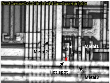
Fig.7: Result from the photoemission observed significant hot spot on the logic cell with 100X lens. The metals level still found adequate for front side analysis since the faulty cell not blocked.
The IDD scanning test found competent to sensitize the faulty logic circuit during the test [10]. Figure 7 shows an anomalous hot spot been detected on the defective IC during the fault localization step. From the observation, the emission spot found on top of poly-silicon (gate) strip demonstrated as a symptom of the oxide defect.
V.EMISSIONCHARACTERIZATION ANDPHYSICAL
ANALYSIS
From the fault localization result, the obtained emission profile plotted with intensity profile vs. spatial resolution of the pixel chart as shown on Figure 8. The high intensity radiated localized from fault M3 p-Ch MOS after performing crosscheck with Cadence LVS tool. The emission well indicated the present of leakage current on faulty IC during the test.
0 20 40 60 80 100 120 0
50 100 150 200 250
M0 M8
M2 M7 M3
in
te
n
s
it
y
(a
.u
)
spatial position (pixel) nMOS pMOS Emission profile on the OR cell during the test
M6
Fig.8: P-Ch. M3 MOS showing high radiation from the excessive current generation.
[image:4.612.73.256.125.263.2]Physical analysis has also done with chemical by remove completely undesired layers (metal interconnection) in order to understand the correlation between the observed emission spot and the physically defect. Figure 9 shows the details of the gate oxide defect observed by the Field-Emission Scanning Electron Microscope (FE-SEM) after poly-silicon strip been removed.
Fig.9: Result from the physical analysis observed pinhole defect on the p-Ch MOS after poly-gate removed.
The morphology and the dimension of the gate oxide short (pinhole defect) was examined using FE-SEM equipment. Figure 9 shows the measured pinhole value and it was found greater than the SiO2 thickness itself. Originally, the pinhole size can predicted smaller from the measured value. During the physical analysis, it had been expanding further consequence from the chemical reaction on the oxide layer during earlier etching step at poly silicon.
Nevertheless, for precise topology view of the defect can obtain by using Focus Ion Beam (FIB) equipment, which well effective presenting vertical view of the desire area without modifying the originality of the pinhole defect size.
Based on the physical analysis result, it was confirmed the short having high possibility induced by the time dependent dielectric breakdown models (TDDB). Through the TDDB models, the failure may originates by grounds of; the local thinning of thin oxide layer, which degraded during the fabrication process or by hot electron orientation, whereas more electrons attract and trapped into oxide, then accumulate until reaching the attracted final breakdown [11, 12].
VI. CONCLUSIONS
In this research, we have shown the failure analysis technique for gate oxide defect of CMOS VLSI on the ASIC device. Gate oxide (SiO2) defect is a time dependence defect and this paper successfully reveals experimentation on the failure of IC that suffers from field application. An abnormal emission being spotted and characterize based on the elevated IDD current on the fault cell during the logic transition. Therefore, IDD scan test technique was effective to localize faulty IC in silicon active area fault through front side FA.
Metal3 Metal2
Metal1
Hot spot
240nm: pinhole
28nm: thickness Poly strip
[image:4.612.317.544.135.283.2] [image:4.612.66.296.513.643.2]However, we should note that this method may ineffectively apply with 65nm to lower scale of technologies. Since lower drain bias voltages will be applied for the CMOS in this scale to be worked, i.e. 1.8v, 1.3v or 0.7v, the unsurprising elevated current in the test circuit can be much smaller, in range of Nano to Pico ampere, or even impossible to discriminate if the defect in actual circuit having direct impact to the current generation or not. The influences from the input frequency for high speed circuit also need to be considered. It might create blockade to determine the correlation between the defect and the how much current value elevated inside the circuit during every single CMOS transition time during electrical stimulus. At this point, fault localization may become mystified to breakthrough.
In other hand, for higher scaled technologies, even through the gate length may reduce to few nm with oxide thickness <1nm, the current leakage between the gate and the channel may occur by quantum tunneling effect. This may cost the fault localization and isolation techniques become more complex if depend solely on the elevated or quiescent current values. Therefore, the proposal of future work is to study the estimate current measurement for the lower technology scale which may facilitate to distinguish between fault-free IC and faulty one. The experimentation can be achieved at software level via circuit simulation with technology library support.
Since the interconnection dense and levels increasing by technology complexity, sample preparation has to innovate for backside failure analysis. This method highly recommends overcoming the disadvantages of conventional front-side failure analysis. Through this advance, silicon area can be access without terrified of losing signal strength due to impediment by the metal line or refractive index of silicon layer. As a benefit, equipment sensitivity may amplify significantly to localizing the defect.
ACKNOWLEDGMENT
The authors would like to thanks members of ST Microelectronics failure analysis laboratory and Microelectronics and Nanotechnology – Shamsuddin Research Centre (MiNT-SRC) laboratory, UTHM for this research collaboration and discussion.
REFERENCES
[1] BCD Technology devices – Automotive Product Group (APG), ST Microelectronics.
[2] J.McPherson and H.Mogul, “Disturbed bonding states in SiO2 thin-films
and their impact on time-dependence dielectric breakdown,” in International Reliability Physics Symposium (IRPS), pp.47-56, April 1998.
[3] J.H.Suehle, “Ultra thin gate oxide reliability: physical model, statistic, and characterization,” IEEE Trans. Electron Devices, vol.49. 958-971, June 2002.
[4] Colm Durkan “Current At The Nanoscale – An Introduction To Nanoelectronics”, Imperial College Pres, Pages 32-35, 44-46.
[5] J.Segura, C.Benito, A Rubio and C.F. Hawkins, “A Detailed Analysis of GOS Defects in MOS Transistors: Testing Implications at Circuit Level,” Proceedings of International Test Conference, 1995, pp.544-551. [6] Ian A.Grout: “Integrated Circuit Test Engineering”, Springer, pages
62-65, 70-73.
[7] C.F Hawkins, J.M Soden, “Reliability and Electrical Properties of Gate Oxide Short in CMOS IC Testing”, Proceedings of International Test Conference, 1994, pp.413-425.
[8] David P.Vallet: “Failure Analysis Requirement for Nanoelectronics” IEEE Transactions On Nanotechnology,Vol. 1, No. 3, September 2002. [9] User Manual, Hamamatsu PHEMOS-1000 Photonics K.K. Document
number: 55340-110-12.
[10] Farisal Abdullah, Nafarizal Nayan, Muhammad Mahadi Abdul Jamil, Norfauzi Kamsin: “IDD scan test method for fault localization technique
on CMOS VLSI failure analysis,” 9th
ICSE Proc. 2010, Melaka, Malaysia
[11] D.J. DUMIN “Oxide Wearout, Breakdown, and Reliability”, International Journal of High Speed Electronics and System, Vol.11, No.3 (2001) , pp.617-718.